
A Broadband Polarization-Insensitive Graphene Modulator Based on Dual Built-in Orthogonal Slots Plasmonic Waveguide

 , and
, and
Abstract
1. Introduction
2. Configuration and Structure
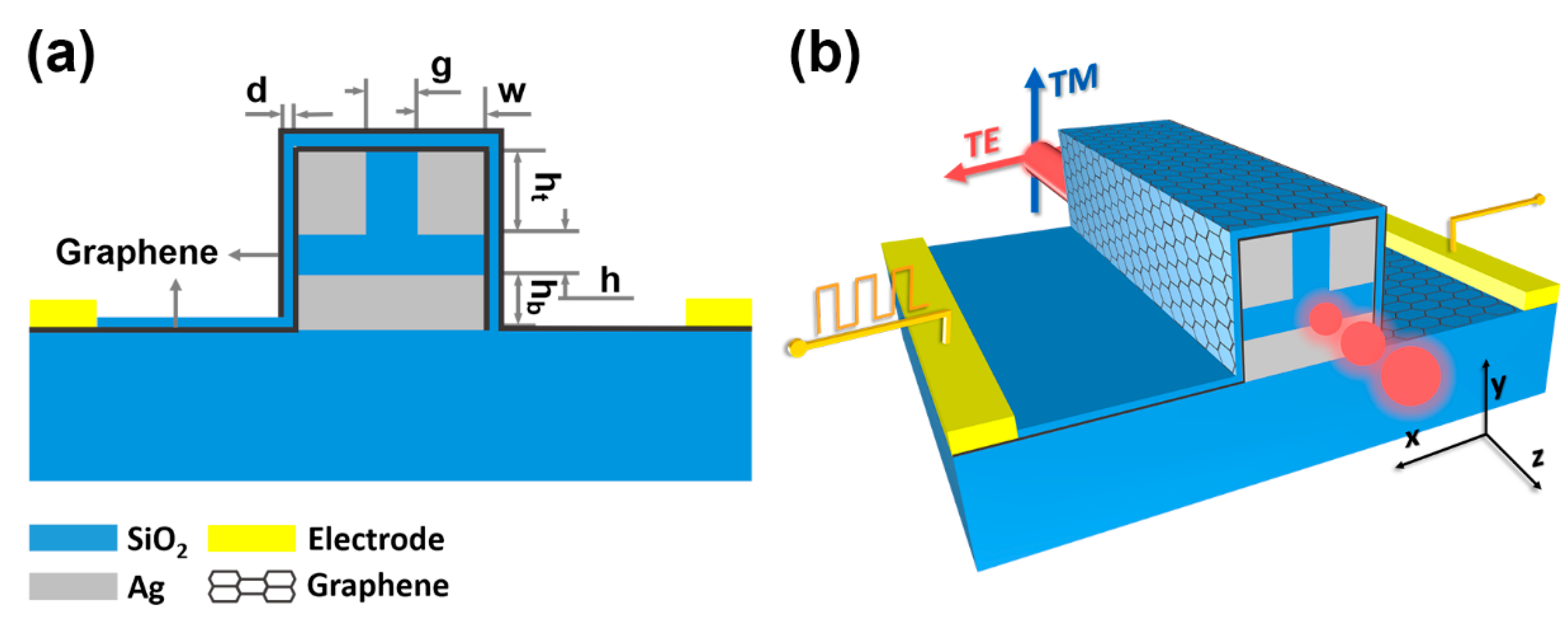
2.1. Device Structure
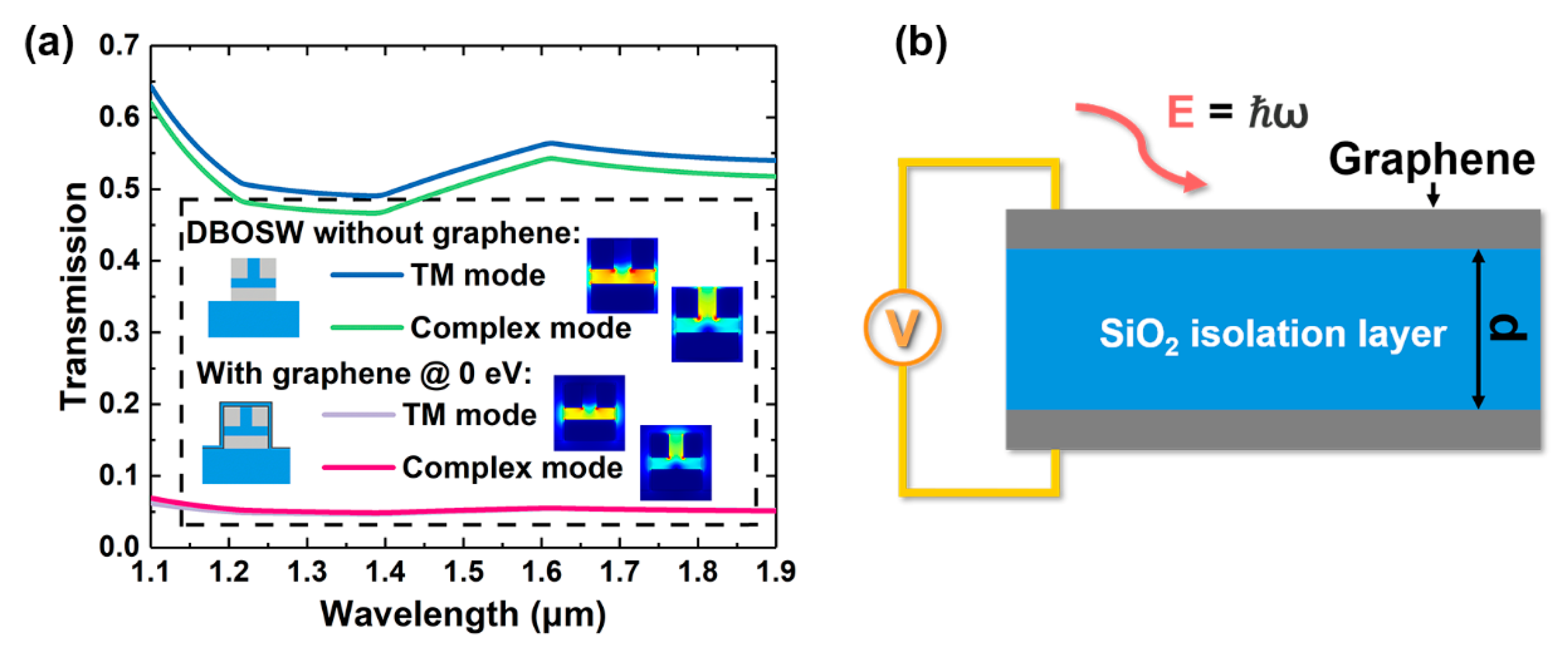
2.2. Graphene Film
3. Design Optimization
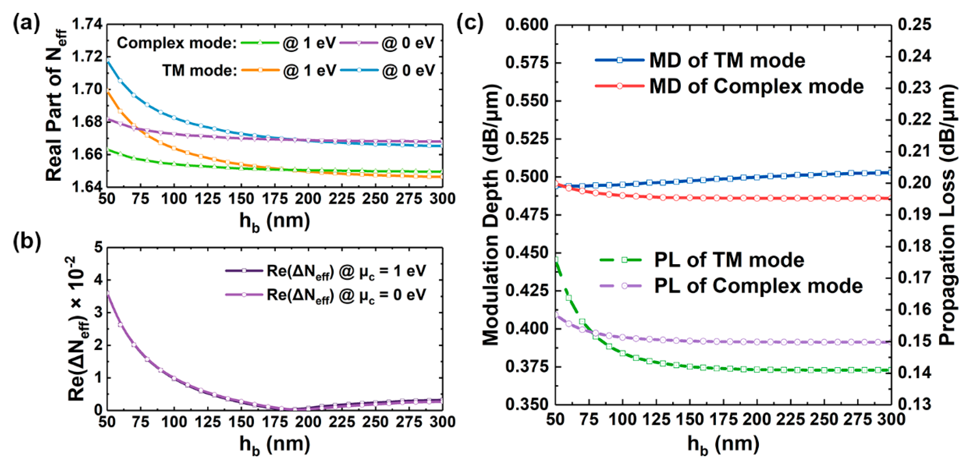
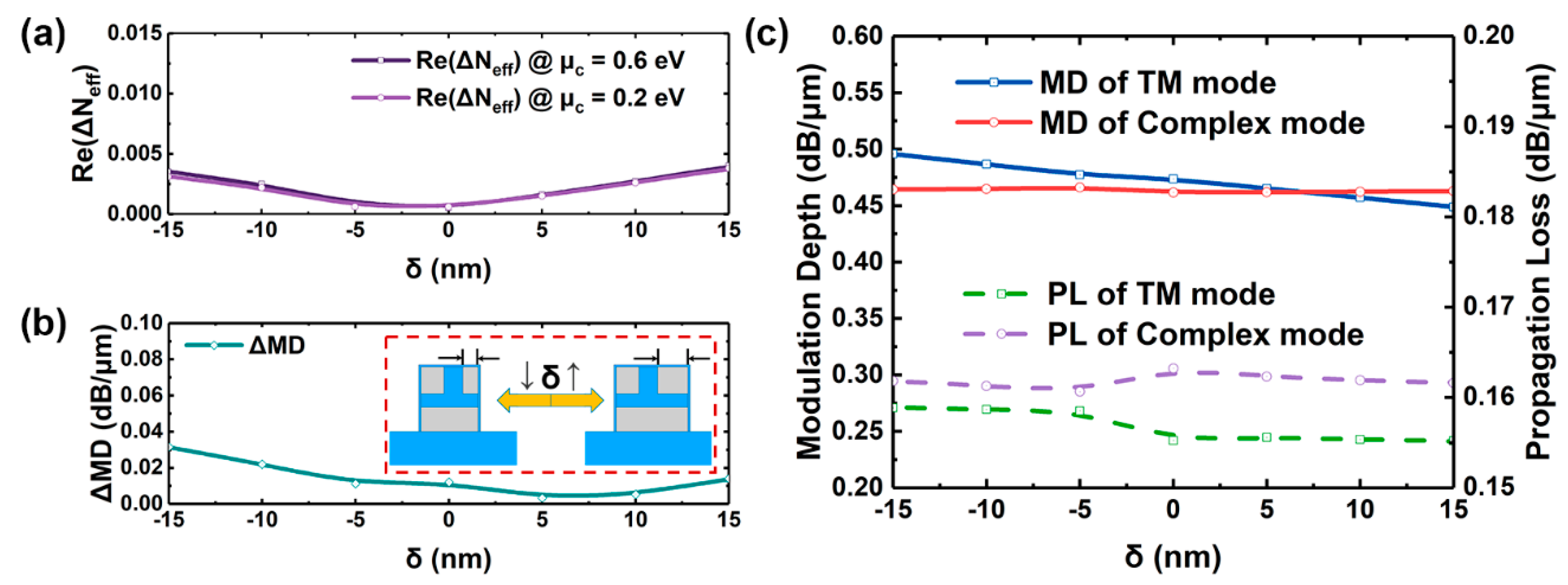
3.1. hb
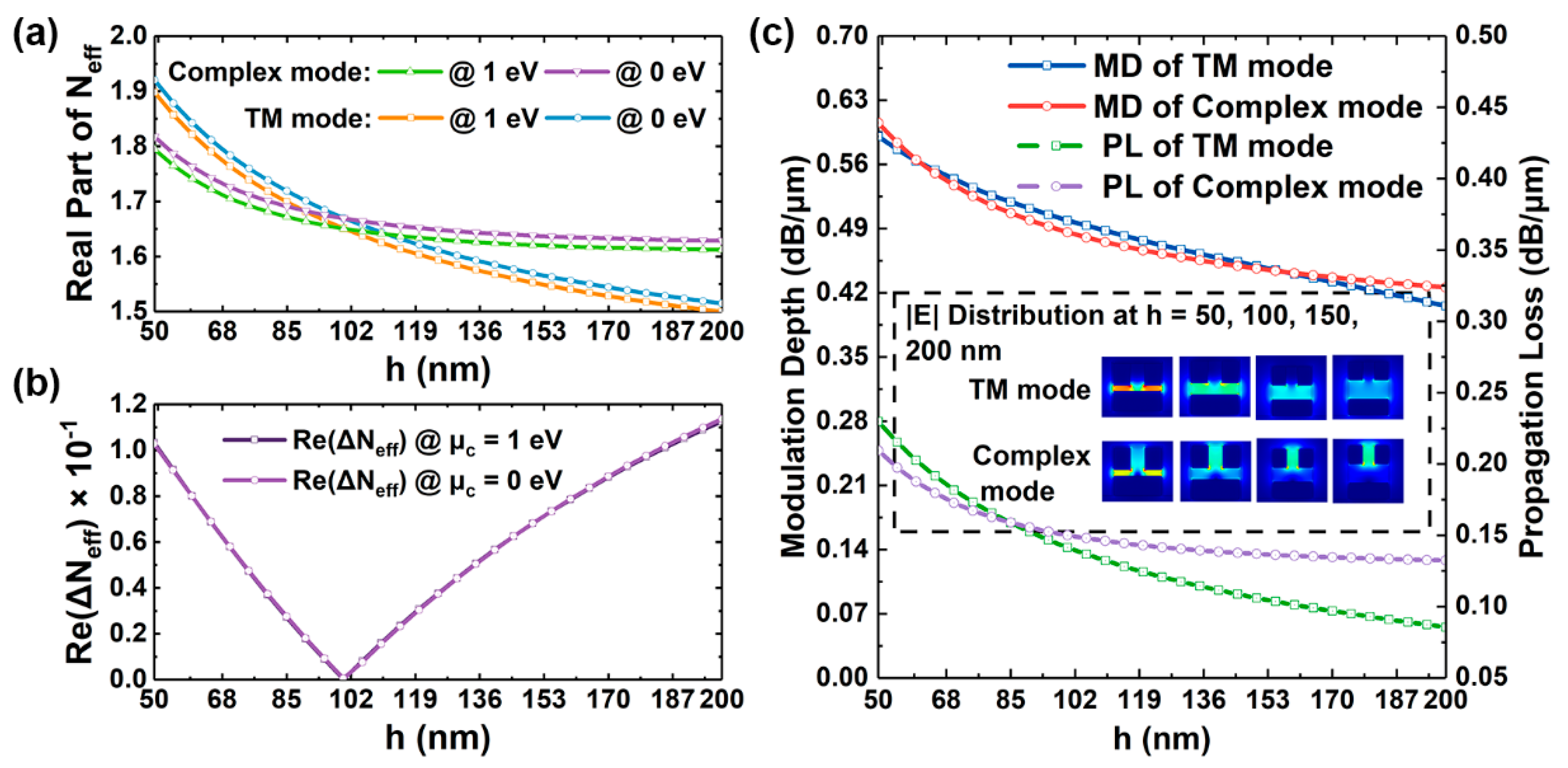
3.2. h
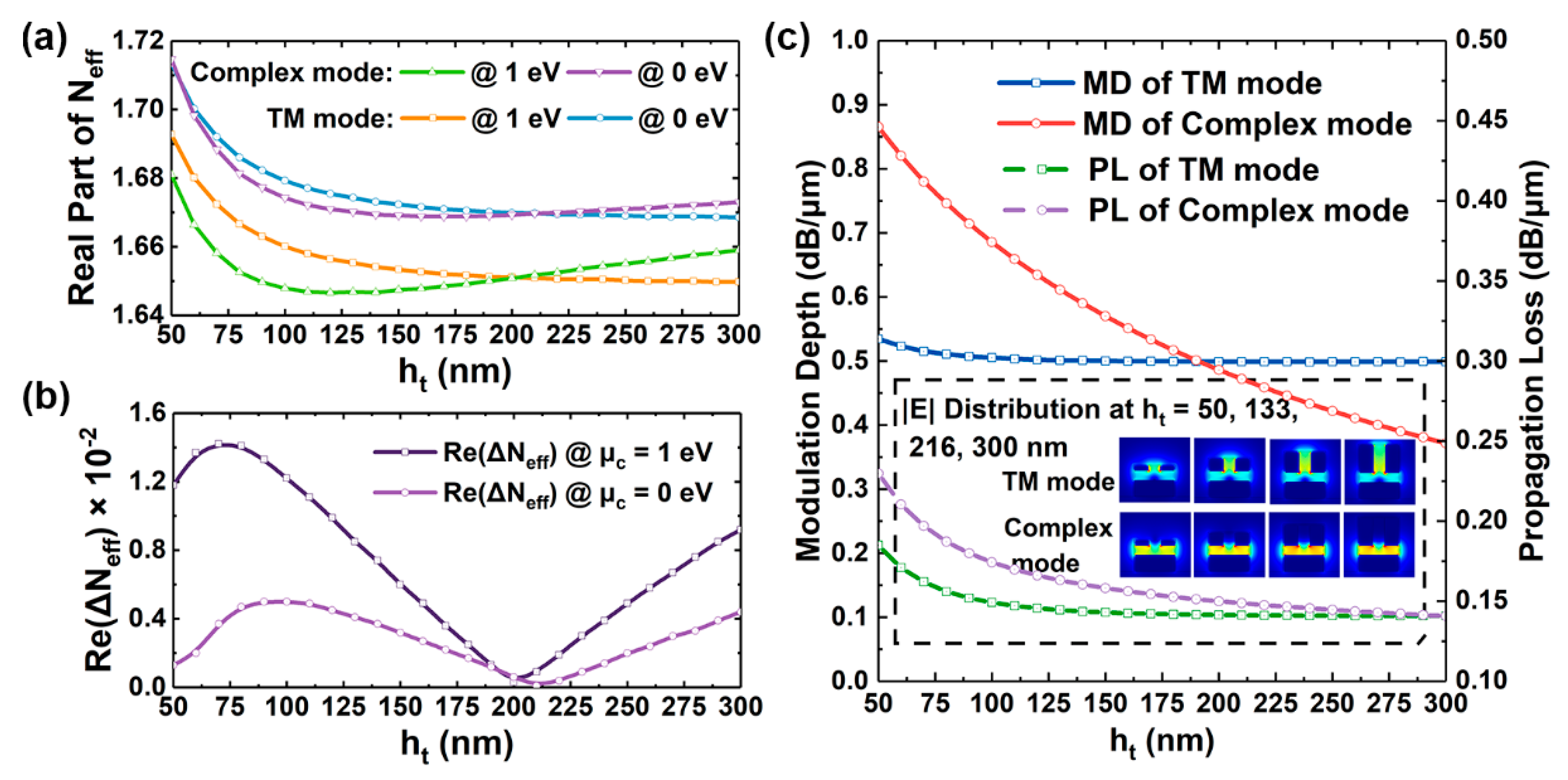
3.3. ht
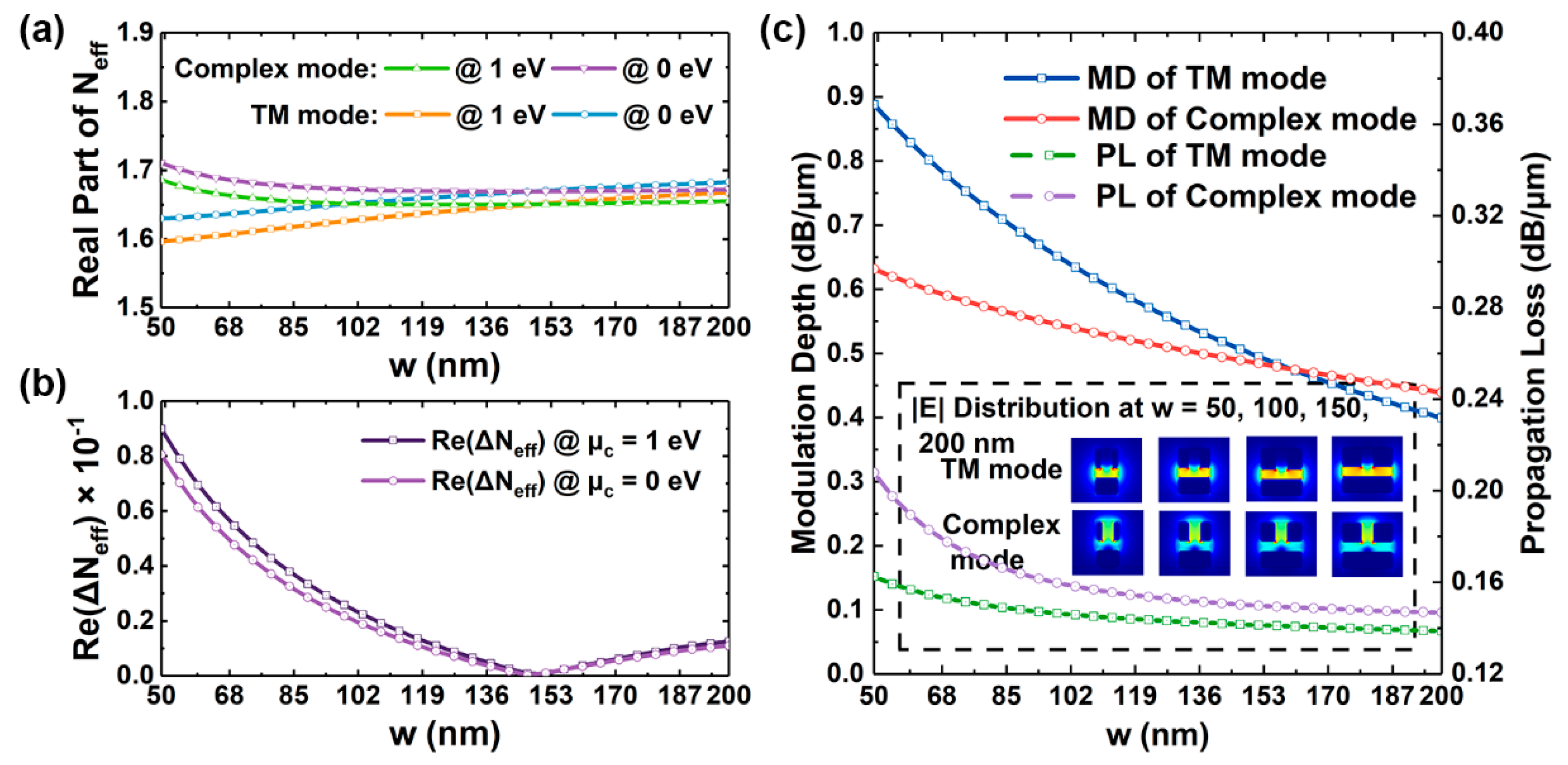
3.4. w
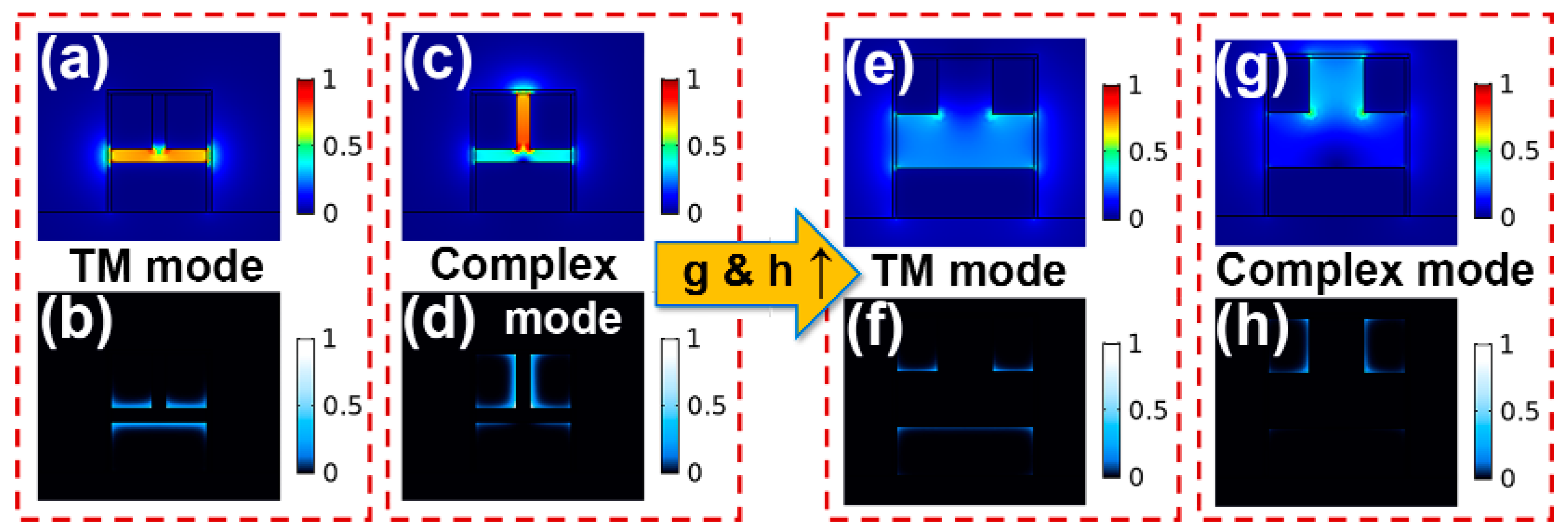
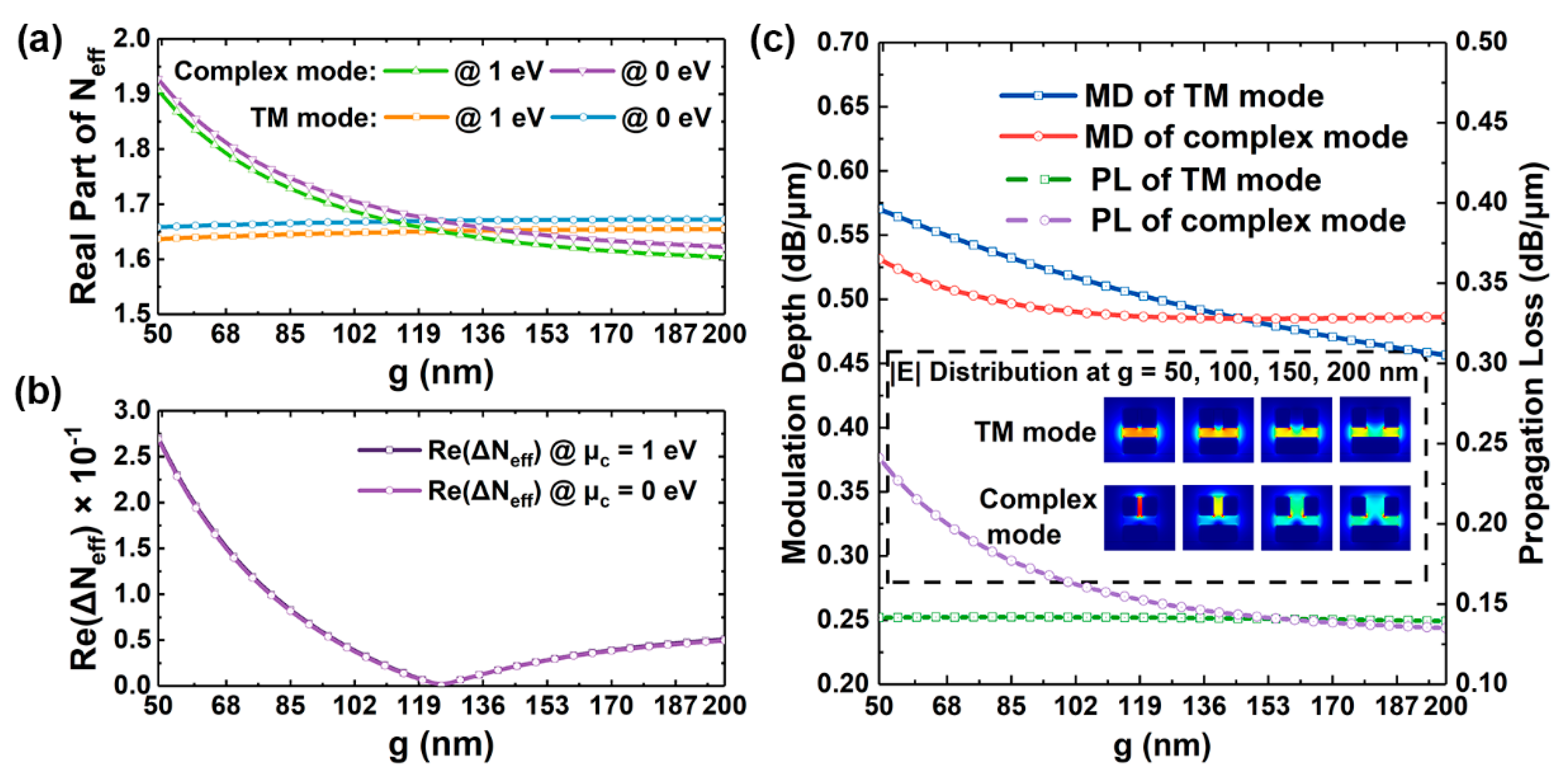
3.5. g
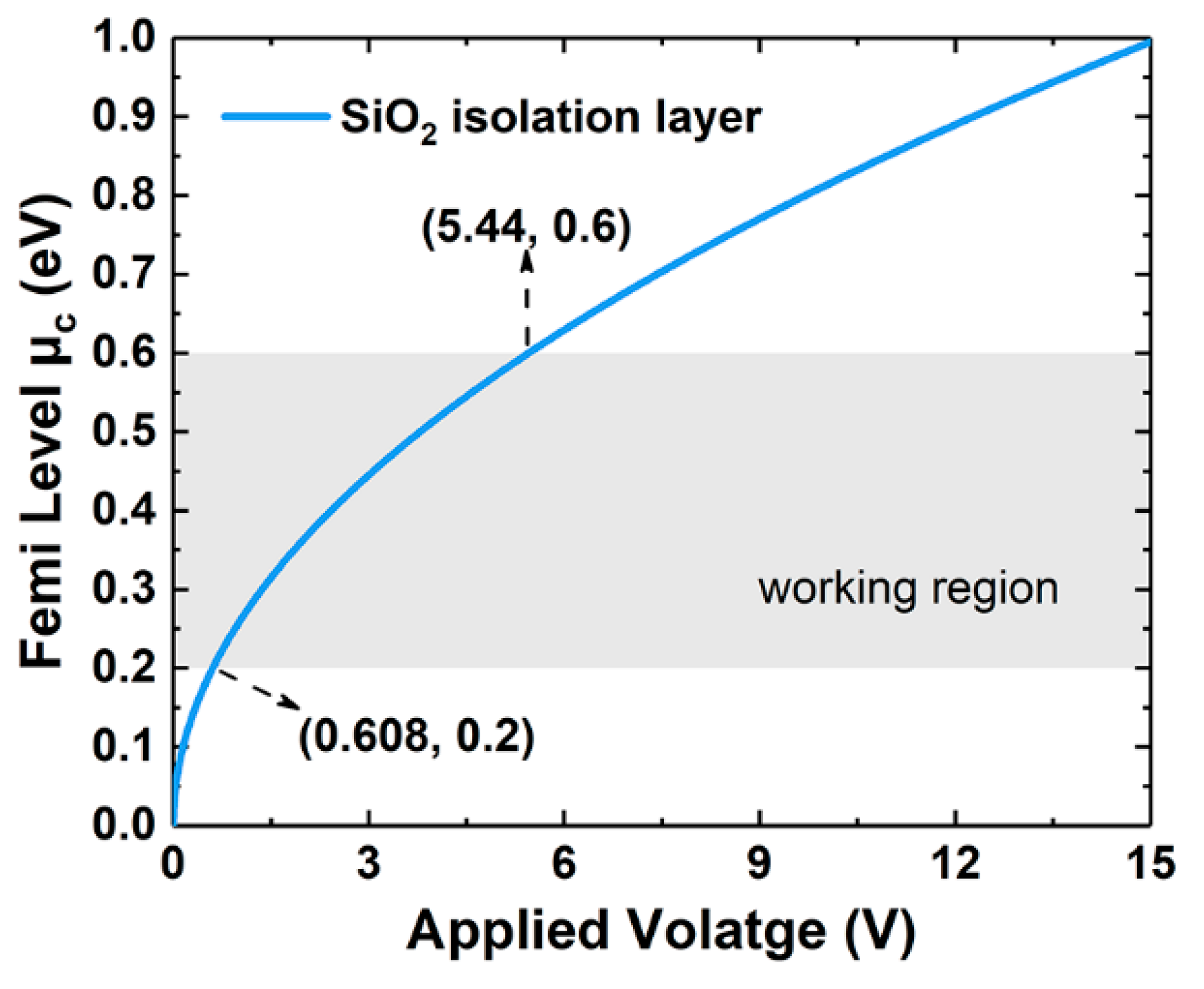
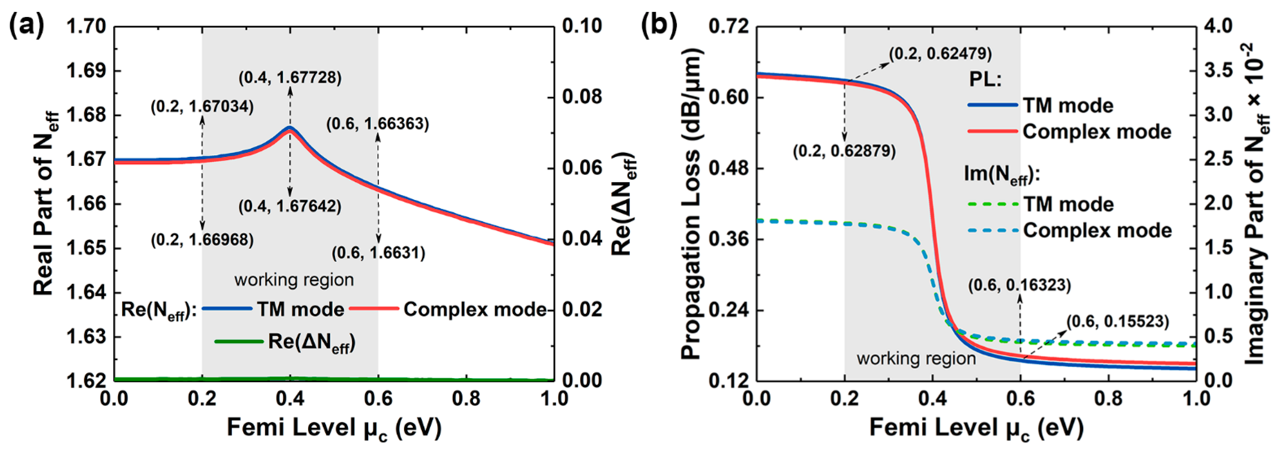
3.6. μc Response
4. Performance and Discussion
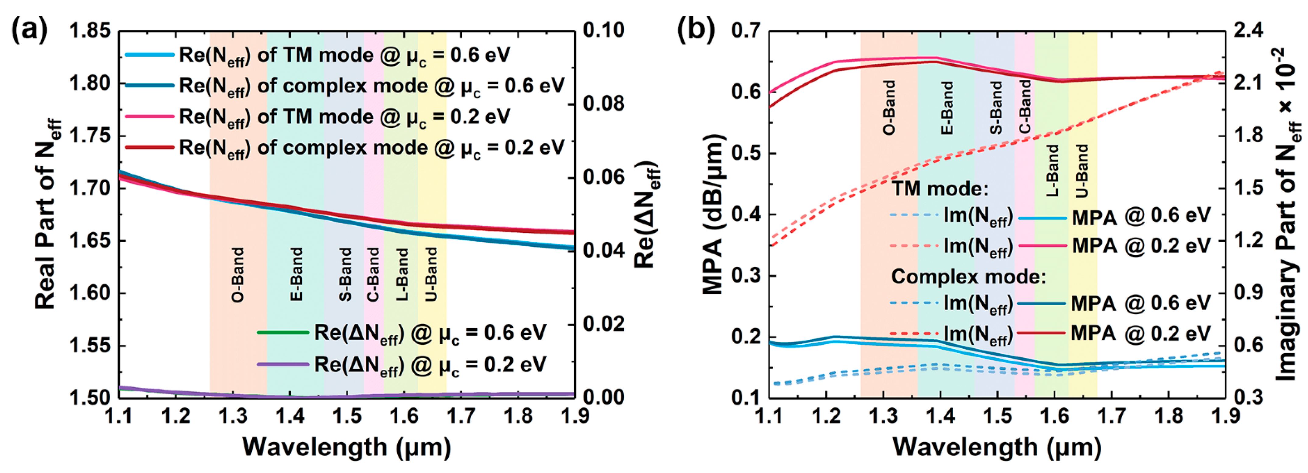
4.1. Optical Bandwidth
4.2. Frequency Response
5. Conclusions
Author Contributions
Funding
Institutional Review Board Statement
Informed Consent Statement
Conflicts of Interest
References
- Marris-Morini, D.; Lyan, P.; Rivallin, P.; Halbwax, M.; Laval, S.; Vivien, L.; Rasigade, G.; Fedeli, J.-M.; Cassan, E.; Le Roux, X.; et al. Recent Progress in High-Speed Silicon-Based Optical Modulators. Proc. IEEE 2009, 97, 1199–1215. [Google Scholar] [CrossRef]
- Wang, C.; Zhang, M.; Chen, X.; Bertrand, M.; Shams-Ansari, A.; Chandrasekhar, S.; Winzer, P.; Lončar, M. Integrated lithium niobate electro-optic modulators operating at CMOS-compatible voltages. Nature 2018, 562, 101–104. [Google Scholar] [CrossRef] [PubMed]
- Pérez-Galacho, D.; Marris-Morini, D.; Stoffer, R.; Cassan, E.; Vivien, L. Simplified modeling and optimization of silicon modulators based on free-carrier plasma dispersion effect. Opt. Express 2016, 24, 26332–26337. [Google Scholar] [CrossRef]
- Park, J.-K.; Takagi, S.; Takenaka, M. InGaAsP Mach–Zehnder interferometer optical modulator monolithically integrated with InGaAs driver MOSFET on a III-V CMOS photonics platform. Opt. Express 2018, 26, 4842–4852. [Google Scholar] [CrossRef]
- Nickelson, L.; Gric, T.; Asmontas, S.; Martavicius, R. Electric Field Distributions of the Fast and Slow Modes Propagated in the Open Rod SiC Waveguide. Elektron. Elektrotech. 2009, 93, 87–90. [Google Scholar]
- Hu, Y.; Pantouvaki, M.; Van Campenhout, J.; Brems, S.; Asselberghs, I.; Huyghebaert, C.; Absil, P.; Van Thourhout, D. Broadband 10 Gb/s operation of graphene electro-absorption modulator on silicon. Laser Photon. Rev. 2016, 10, 307–316. [Google Scholar] [CrossRef]
- Mohsin, M.; Schall, D.; Otto, M.; Noculak, A.; Neumaier, D.; Kurz, H. Graphene based low insertion loss electro-absorption modulator on SOI waveguide. Opt. Express 2014, 22, 15292–15297. [Google Scholar] [CrossRef]
- Dalir, H.; Xia, Y.; Wang, Y.; Zhang, X. Athermal Broadband Graphene Optical Modulator with 35 GHz Speed. ACS Photonics 2016, 3, 1564–1568. [Google Scholar] [CrossRef]
- Phatak, A.; Cheng, Z.Z.; Qin, C.Y.; Goda, K. Design of electro-optic modulators based on graphene-on-silicon slot waveguides. Opt. Lett. 2016, 41, 2501–2504. [Google Scholar] [CrossRef] [PubMed]
- Liu, M.; Yin, X.; Ulin-Avila, E.; Geng, B.; Zentgraf, T.; Ju, L.; Wang, F.; Zhang, X. A graphene-based broadband optical modulator. Nature 2011, 474, 64–67. [Google Scholar] [CrossRef]
- Liu, M.; Yin, X.; Zhang, X. Double-Layer Graphene Optical Modulator. Nano Lett. 2012, 12, 1482–1485. [Google Scholar] [CrossRef]
- Phare, C.T.; Daniel Lee, Y.-H.; Cardenas, J.; Lipson, M. Graphene electro-optic modulator with 30 GHz bandwidth. Nat. Photonics 2015, 9, 511–514. [Google Scholar] [CrossRef]
- Schuller, J.A.; Barnard, E.S.; Cai, W.; Jun, Y.C.; White, J.S.; Brongersma, M.L. Plasmonics for extreme light concentration and manipulation. Nat. Mater. 2010, 9, 193–204. [Google Scholar] [CrossRef]
- Bozhevolnyi, S.I.; Volkov, V.S.; Devaux, E.; Laluet, J.Y.; Ebbesen, T.W. Channel plasmon subwavelength waveguide components including interferometers and ring resonators. Nature 2006, 440, 508–511. [Google Scholar] [CrossRef] [PubMed]
- Gramotnev, D.K.; Bozhevolnyi, S.I. Plasmonics beyond the diffraction limit. Nat. Photonics 2010, 4, 83–91. [Google Scholar] [CrossRef]
- Huang, B.-H.; Lu, W.-B.; Li, X.-B.; Wang, J.; Liu, Z.-G. Waveguide-coupled hybrid plasmonic modulator based on graphene. Appl. Optics 2016, 55, 5598–5602. [Google Scholar] [CrossRef] [PubMed]
- Zheng, P.; Yang, H.; Fan, M.; Hu, G.; Zhang, R.; Yun, B.; Cui, Y. A Hybrid Plasmonic Modulator Based on Graphene on Channel Plasmonic Polariton Waveguide. Plasmonics 2018, 13, 2029–2035. [Google Scholar] [CrossRef]
- Bao, Q.; Zhang, H.; Wang, B.; Ni, Z.; Lim, C.H.Y.X.; Wang, Y.; Tang, D.Y.; Loh, K.P. Broadband graphene polarizer. Nat. Photonics 2011, 5, 411–415. [Google Scholar] [CrossRef]
- Chang, L.-M.; Liu, L.; Gong, Y.-H.; Tan, M.-Q.; Yu, Y.-D.; Li, Z.-Y. Polarization-independent directional coupler and polarization beam splitter based on asymmetric cross-slot waveguides. Appl. Optics 2018, 57, 678–683. [Google Scholar] [CrossRef]
- Zhong, H.; Zhang, Z.Y.; Chen, B.Y.; Xu, H.T.; Yu, D.M.; Huang, L.; Peng, L.M. Realization of low contact resistance close to theoretical limit in graphene transistors. Nano Res. 2015, 8, 1669–1679. [Google Scholar] [CrossRef]
- Veronis, G.; Fan, S. Modes of Subwavelength Plasmonic Slot Waveguides. J. Lightwave Technol. 2007, 25, 2511–2521. [Google Scholar] [CrossRef]
- Geim, A.K.; Novoselov, K.S. The rise of graphene. Nat. Mater. 2009, 6, 183–191. [Google Scholar] [CrossRef]
- Schwierz, F. Graphene transistors. Nat. Nanotechnol. 2010, 5, 487–496. [Google Scholar] [CrossRef] [PubMed]
- Bonaccorso, F.; Hasan, T.; Sun, Z.; Ferrari, A.C. Graphene photonics and optoelectronics. Nat. Photonics 2010, 4, 611–622. [Google Scholar] [CrossRef]
- Kusuma, J.; Balakrishna, R.G.; Patil, S.; Jyothi, M.S.; Chandan, H.R.; Shwetharani, R. Exploration of graphene oxide nanoribbons as excellent electron conducting network for third generation solar cells. Solar Energy Mater. Solar Cells 2018, 183, 211–219. [Google Scholar] [CrossRef]
- Avouris, P.; Chen, Z.; Perebeinos, V. Carbon Based Electronics. Nat. Nanotechnol. 2007, 2, 605–615. [Google Scholar] [CrossRef] [PubMed]
- Bolotin, K.I.; Sikes, K.J.; Jiang, Z.; Klima, M.; Fudenberg, G.; Hone, J.; Kim, P.; Stormer, H.L. Ultrahigh electron mobility in suspended graphene. Solid State Commun. 2008, 146, 351–355. [Google Scholar] [CrossRef]
- Nair, R.R.; Blake, P.; Grigorenko, A.N.; Novoselov, K.S.; Booth, T.J.; Stauber, T.; Peres, N.M.R.; Geim, A.K. Fine Structure Constant Defines Visual Transparency of Graphene. Science 2008, 320, 1308. [Google Scholar] [CrossRef] [PubMed]
- Mak, K.F.; Sfeir, M.Y.; Wu, Y.; Lui, C.H.; Misewich, J.A.; Heinz, T.F. Measurement of the Optical Conductivity of Graphene. Phys. Rev. Lett. 2008, 101, 196405–196408. [Google Scholar] [CrossRef] [PubMed]
- Sensale-Rodriguez, B.; Yan, R.; Kelly, M.M.; Fang, T.; Tahy, K.; Hwang, W.S.; Jena, D.; Liu, L.; Xing, H.G. Broadband graphene terahertz modulators enabled by intraband transitions. Nat. Commun. 2012, 3, 780–786. [Google Scholar] [CrossRef]
- Gric, T.; Nickelson, L.; Asmontas, S. Electrodynamical characteristic particularity of open metamaterial square and circular waveguides. Prog. Electromagn. Res. 2010, 109, 361–379. [Google Scholar] [CrossRef][Green Version]
- Ye, L.; Sui, K.; Zhang, Y.; Liu, Q.H. Broadband optical waveguide modulators based on strongly coupled hybrid graphene and metal nanoribbons for near-infrared applications. Nanoscale 2019, 11, 3229–3239. [Google Scholar] [CrossRef] [PubMed]
- Hanson, G.W. Dyadic Green’s functions and guided surface waves for a surface conductivity model of graphene. J. Appl. Phys. 2007, 103, 064302–064309. [Google Scholar] [CrossRef]
- Kwon, M.-S. Discussion of the Epsilon-Near-Zero Effect of Graphene in a Horizontal Slot Waveguide. IEEE Photonics J. 2014, 6, 1–9. [Google Scholar] [CrossRef]
- Hwang, C.; Siegel, D.A.; Mo, S.K.; Regan, W.; Ismach, A.; Zhang, Y.; Zettl, A.; Lanzara, A. Fermi velocity engineering in graphene by substrate modification. Sci. Rep. 2012, 2, 590–593. [Google Scholar] [CrossRef]
- Ding, Y.; Guan, X.; Zhu, X.; Hao, H.; Xiao, S. Effective electro-optic modulation in low-loss graphene-plasmonic slot waveguides. Nanoscale 2017, 9, 15576–15581. [Google Scholar] [CrossRef]
- Hu, Y.; Xiao, X.; Xu, H.; Li, X.; Xiong, K.; Li, Z.; Chu, T.; Yu, Y.; Yu, J. High-speed silicon modulator based on cascaded microring resonators. Opt. Express 2012, 20, 15079–15085. [Google Scholar] [CrossRef]
- Abdollahi Shiramin, L.; Van Thourhout, D. Graphene Modulators and Switches Integrated on Silicon and Silicon Nitride Waveguide. IEEE J. Sel. Top. Quantum Electron. 2016, 23, 94–100. [Google Scholar] [CrossRef]
- Yang, Z.; Lu, R.; Cai, S.; Wang, Y.; Zhang, Y.; Wang, X.; Liu, Y. A CMOS-compatible and polarization-insensitive graphene optical modulator. Opt. Commun. 2019, 450, 130–135. [Google Scholar] [CrossRef]
- Yang, Z.; Lu, R.; Wang, Y.; Cai, S.; Zhang, Y.; Wang, X.; Liu, Y. A fabrication-friendly graphene-based polarization insensitive optical modulator. Optik 2019, 182, 1093–1098. [Google Scholar] [CrossRef]
- Shirdel, M.; Mansouri-Birjandi, M.A. Broadband graphene modulator based on a plus-shaped plasmonic slot waveguide. Appl. Optics 2019, 58, 8174–8179. [Google Scholar] [CrossRef]
- Hu, X.; Wang, J. Design of graphene-based polarization-insensitive optical modulator. Nanophotonics 2018, 7, 651–658. [Google Scholar] [CrossRef]
- Xu, Y.; Li, F.; Kang, Z.; Huang, D.; Zhang, X.; Tam, H.-Y.; Wai, P. Hybrid Graphene-Silicon Based Polarization-Insensitive Electro-Absorption Modulator with High-Modulation Efficiency and Ultra-Broad Bandwidth. Nanomaterials 2019, 9, 157–171. [Google Scholar] [CrossRef] [PubMed]
- Ye, S.W.; Liang, D.; Lu, R.-G.; Shah, M.K.; Zou, X.-H.; Yang, F.; Yuan, F.; Liu, Y. Polarization Independent Modulator by Partly Tilted Graphene Induced Electro-Absorption Effect. IEEE Photonics Technol. Lett. 2016, 29, 23–26. [Google Scholar] [CrossRef]
- Zou, X.H.; Zhang, Y.J.; Li, Z.H.; Yang, Y.W.; Zhang, S.J.; Zhang, Z.Y.; Zhang, Y.L.; Liu, Y. Polarization-Insensitive Phase Modulators Based on an Embedded Silicon-Graphene-Silicon Waveguide. Appl. Sci.-Basel 2019, 9, 429–436. [Google Scholar] [CrossRef]


| Ref. | Bandwidth (nm) | Re(ΔNeff) | MD (dB/μm) | ΔMD (dB/μm) | f3dB(GHz) | Ebit(fJ/bit) |
| [39] | 1500–1600 | - | 0.06 | 0 | 13.4 | - |
| [40] | 1500–1600 | - | 0.08 | 0 | 80 | - |
| [41] | 1200–1600 | - | mode A: 1.05, mode B: 1.13, mode C: 0.52 | Min: 0.08 Max: 0.61 | 95 | 138.8 |
| [42] | 1530–1565 | 4.7 × 10⁻³ | TM mode: ~0.2975, TE mode: ~0.2895 | ~8 × 10⁻³ | 30.2 | 2980 |
| [43] | 1367–1771 | ~0.5 | TM mode: 1.113, TE mode: 1.119 | ~6 × 10⁻³ | 6.1 | 7800 |
| [44] | 1450– 1650 | ~0.1 | TM mode: 1.392, TE mode: 1.347 | 0.045 | ~100 | - |
| [45] | 1300–1800 | 1.2 × 10⁻³ | - | - | 135.6 | - |
| This work | 1100–1900 | 6 × 10⁻⁴ | TM mode: 0.474, complex mode: 0.462 | 0.012 | 101 | 271 |
Publisher’s Note: MDPI stays neutral with regard to jurisdictional claims in published maps and institutional affiliations. |
© 2021 by the authors. Licensee MDPI, Basel, Switzerland. This article is an open access article distributed under the terms and conditions of the Creative Commons Attribution (CC BY) license (http://creativecommons.org/licenses/by/4.0/).
Share and Cite
Chen, W.; Xu, Y.; Gao, Y.; Ji, L.; Wang, X.; Sun, X.; Zhang, D. A Broadband Polarization-Insensitive Graphene Modulator Based on Dual Built-in Orthogonal Slots Plasmonic Waveguide. Appl. Sci. 2021, 11, 1897. https://doi.org/10.3390/app11041897
Chen W, Xu Y, Gao Y, Ji L, Wang X, Sun X, Zhang D. A Broadband Polarization-Insensitive Graphene Modulator Based on Dual Built-in Orthogonal Slots Plasmonic Waveguide. Applied Sciences. 2021; 11(4):1897. https://doi.org/10.3390/app11041897
Chicago/Turabian StyleChen, Wei, Yan Xu, Yang Gao, Lanjing Ji, Xibin Wang, Xiaoqiang Sun, and Daming Zhang. 2021. "A Broadband Polarization-Insensitive Graphene Modulator Based on Dual Built-in Orthogonal Slots Plasmonic Waveguide" Applied Sciences 11, no. 4: 1897. https://doi.org/10.3390/app11041897
APA StyleChen, W., Xu, Y., Gao, Y., Ji, L., Wang, X., Sun, X., & Zhang, D. (2021). A Broadband Polarization-Insensitive Graphene Modulator Based on Dual Built-in Orthogonal Slots Plasmonic Waveguide. Applied Sciences, 11(4), 1897. https://doi.org/10.3390/app11041897