Article

Effects of Vacancy and Hydrogen on the Growth and Morphology of N-Type Phosphorus-Doped Diamond Surfaces

1
School of Power and Mechanical Engineering, Wuhan University, Wuhan 430072, China
2
Research Institute of Wuhan University in Shenzhen, Shenzhen 518057, China
3
School of Logistic Engineering, Wuhan University of Technology, Wuhan 430070, China
*
Authors to whom correspondence should be addressed.
Appl. Sci. 2021, 11(4), 1896; https://doi.org/10.3390/app11041896
Submission received: 1 February 2021 / Revised: 14 February 2021 / Accepted: 17 February 2021 / Published: 22 February 2021
(This article belongs to the Section Applied Physics General)

Abstract

:
Phosphorus is regarded as the best substitutional donor for n-type diamonds. However, because of vacancy-related complexes, H-related complexes, and other defects in P-doped diamonds, obtaining n-type diamonds with satisfying properties is challenging. In this report, PV and PVH complexes are studied in detail using density function theory (DFT). The formation energy reveals the possibility of emergency of these complexes when doping a single P atom. Although vacancies have difficulty forming on the surface alone, the presence of P atoms benefits the formation of PV and PVH complexes and significantly increases crystal vacancies, especially in (111) diamond surfaces. Compared to (111) surfaces, PV and PVH complexes more easily form on (001) surfaces. However, the formation energies of these complexes on (001) surfaces are higher than those of doping P atoms. Studying the structural deformation demonstrated that both constraints of the upper and lower C layers and forces caused by structural deformation prevented doping P atoms. By analyzing the bond population around these dopants, it finds that the bond populations of P–C bonds of PVH complexes are larger than those of PV complexes, indicating that the PV complexes are not as stable as the PVH complexes.

1. Introduction

Diamonds are third-generation semiconductor materials that are often called ultimate semiconductors. Due to their excellent mechanical, chemical, and electronic properties [1], such as high fracture strength, corrosion resistance, high thermal stability, high breakdown field, and high carrier mobility [2] diamonds have attracted considerable attention in many fields. Doping different impurities in diamond to get the required performance is always a research hotspot, for example the Group-4 vacancy color centers in diamond can be used for quantum communication and sensor application [3]. Wide band gap (5.5 eV) makes diamond an ideal electronic material [1]. By doping donor and acceptor atoms in diamonds, the band gap can be adjusted to obtain p-type or n-type diamonds. P-type diamonds have already been successfully produced by doping with boron atoms and is considered as a mature topic [4]. However, the fabrication of high-quality n-type diamonds remains challenging [5].
Doped impurities in n-type diamonds primarily include lithium (Li), sodium (Na), oxygen (O), nitrogen (N), sulfur (S), and phosphorus (P). They are present in diamonds either as interstitial atoms (such as Li and Na) or substitutional atoms (such as O, N, S, and P) [6]. N, S, and P attracted considerable attention in previous studies [7]. Unlike N, which is proven to be a deep donor with an activation energy of 1.7 eV [8] and S with an activation energy of more than 1 eV and low doping efficiency as demonstrated by theoretical research [9], P with a relatively lower donor level (0.6 eV) is currently considered the best substitutional donor [4]. Theoretical and experimental studies prove that the diamond growth rate appreciably increases as a function of doping phosphorus and thereby reduce the production costs [10]. Koizumi et al. [11] show that n-type diamonds can be successfully produced by doping phosphorus using microwave-enhanced plasma chemical vapor deposition (MPCVD).
However, it is difficult to obtain practical n-type diamonds by doping P atoms. Satio et al. [12] proved that in P-doped (111) diamond surfaces, the carrier concentration and Hall mobility at 500 K are only 3.8 × 108 cm3 and 38 cm2/V, respectively, and the Hall mobility in (001) surfaces is even lower. Koizumi et al. report that the Hall mobility of activated carriers is very low (28 cm2/V at 500 K) and decrease as the temperature decrease (vanishing below 300 K). They suggest that unsatisfactory electrical properties may be due to crystalline imperfections caused by the incorporation of a large amount of P atoms, because crystalline perfection has a significant influence on the electrical properties [11,13]. The Hall mobility vary with the temperature, also suggesting that crystal defects are dominant factors in electron scattering [14]. Through positron lifetime measurement, Dannefaer et al. [15] show that CVD diamond films usually contain a high concentration of vacancies (>50 ppm). The vacancy-related defects in diamonds are commonly considered as deep acceptors that act as strong donor compensation centers. Ideal P-doped diamonds should contain a large amount of P atoms and also be free of vacancies [16]. Therefore, a thorough understanding of the formation and structure of vacancy-related complexes in P-doped diamonds are important and worth studying. H atoms are also the reason for carrier compensation [17]. A large amount of H exists during CVD diamond growth [11,13], and more than 1019 cm−3 of hydrogen is detected on (001) surfaces [18]. It is also necessary to study H-related complexes in detail. Theoretically, the doping mechanisms can be summarized by two methods, doping on the surface and in the crystal [19]. In previous studies, PVxHy complexes in bulk diamonds were carefully investigated [16,20], but PVxHy complexes on growing surfaces still lack detailed research.
Because formation energy of PV and PVH complex is relatively low in bulk diamond [20], indicating that they are more likely to form than other PVxHy complexes, for simplicity, only PV and PVH complexes are considered in this work. The purpose of this study is to investigate the formation of PV and PVH complexes and their influence on the surface structure within diamond (001) and (111) surfaces based on first-principles calculations, since (001) and (111) surfaces are the most commonly used surfaces for doped diamonds. Recently there are many researches in P-doping experiments on (110) surface [21], but as this orientation is difficult to obtain due to its unstable nature during growth, we do not study it in this work. By analyzing the band structure of bulk diamond with PV and PVH complexes, Yan C. X. et al. find that PV complex is an acceptor center providing hole carrier in diamond and PVH complex introduces a deep acceptor level in band gap [
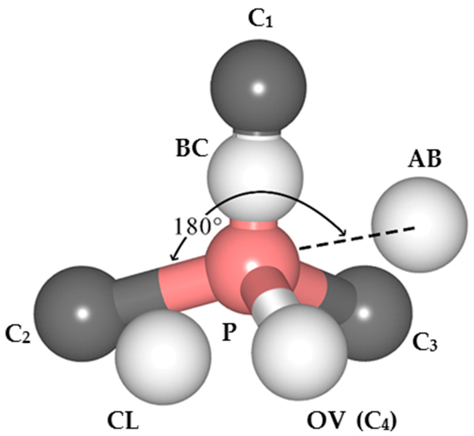
20]. We also investigate doping single P atom and forming single V in diamond surfaces for comparison to reveal the possibility of the emergence of PV and PVH complexes during P atom doping and structural deformation due to vacancies and hydrogen atoms.

2. Materials and Methods

In this study, the Cambridge Sequential Total Energy Package (CASTEP) [22] based on density function theory (DFT) is used for all of the calculations. An ultrasoft pseudopotential [23] plane wave approach is adopted to describe the electrons. The Perdew-Burke-Ernzerhof (PBE) and general gradient approximation (GGA) [24] are used for the exchange–correlation functional. The cutoff energy is 400 eV and the 2 × 2 × 1 k points for both (001) and (111) surfaces are used to sample the Brillouin zone according to the Monkhorst-Pack method [25]. Spin-polarization is taken into consideration [26]. The convergence criterion of the inter-atomic forces is set to be 0.03 eV/ Å, and the energy of self-consistent calculation is 1.0 × 10⁻⁵ eV/atom. The cutoff energy and k points are obtained by careful testing and are proven to be adequate for all of the calculations in this work; higher values of these parameters shows a difference within only 5% in calculation of formation energy.
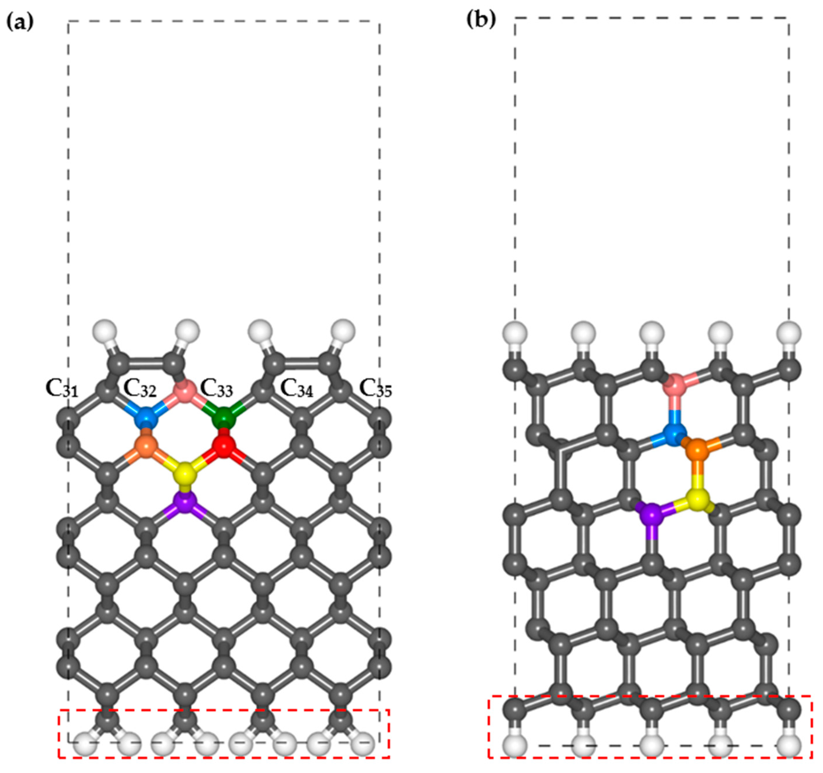
The H-terminated diamond 2 × 1 reconstructed (001) and (111) surfaces are used in this study as they are the most common CVD-growth diamond thin films. A vacuum distance of 10 Å is adopted between the periodical slabs in the z direction to avoid interactions. The numbers of C layers on the (001) and (111) surfaces are 14 and 12, respectively, which are also obtained using the test calculations. The bottom C layer and terminated H layer are constrained to simulate continuous bulk diamonds in the lower region of the surface structure. The calculation parameters and lattice parameters are listed in Table 1.
The formation energy is calculated using the following equation [27,28]:
E f ( P V n H m ) = E ( P V n H m ) E ( p u r e ) [ U p + m U h ( n + 1 ) U c ] q [ E F + E V + Δ V ]
where n and m are the number of vacancies and H atoms, respectively. In this study, it only investigates the situation that they are either zero or one. E ( P V n H m ) and E ( p u r e ) represent the total energy of the diamond surface containing P V n H m and the pure diamond surface, respectively. U p , U h , and U c denote the chemical potentials of P, H, and C, respectively, deduced from their hydrides in gas phase (PH3, H2), and bulk diamonds. q [ E F + E V + Δ V ] is the result of exchanges of electrons or holes with the carrier reservoirs [28]. The following section focuses only on the E F of impurities with neutral charges, so the last term is zero.

3. Results and Discussion

3.1. Formation Energy

DFT calculation results can provide theoretical explanations and reasonable predictions for many experimental phenomena. In this section, the formation energies of the PV, and PVH complexes from the second to sixth C layers are carefully calculated. The formation energy is used to evaluate the quantity and forming efficiency of different complexes. For a more comprehensive comparison, the formation energies of a single P atom and vacancy are also calculated.

3.1.1. Formation Energies of the Single P Atom and Single V

The substitutional location of the P atom and V are shown in Figure 1. These positions are found based on the structural symmetry of the (001) and (111) surface structures. For example, the five outermost atoms in the third C layer of the (001) surface shown in Figure 1a are defined as C31, C32, C33, C34, and C35, respectively. C31, C33, and C35 as well as C32 and C34 are symmetrical, but C31/33/35 and C32/34 are asymmetrical, so the third layer of the (001) surface structure has two doping sites (C31/33/35 and C32/34) with different properties. We define these two sites as 3A and 3B, in which the number represents the doping layer and the capital letter (A and B) refers to the two different doping sites in this layer. Similarly, the doping sites in other layers are defined as 2A, 4A, 4B, 5A, and 6A, respectively. The formation energies of a single P atom and a single V on the (001) and (111) surfaces are shown in Figure 2.
As shown in Figure 2, the lowest formation energy of the single P atom on the (001) and (111) surfaces increases with the number of C layers. This may be the result of structural distortion. Since the volume of a P atom is larger than the volume of a C atom, when a P atom replaces a C atom on the diamond surface, it has the tendency to cause expansive distortions of the surrounding lattice and introduces strain to the system, like doping a europium atom in bulk diamond [29]. When P atom is doped in the upper layer, P has a tendency to move upwards towards the vacuum place, which reduces damage to the underlying structure. Conversely, when the P atom is doped at deeper layers, the formation energy significantly increases because it has to destroy the surrounding structure. In addition, regarding the formation energies of the P atom in site A and B in the third and fourth layers of the (001) surface, the energy of the site A is significantly higher than that of the site B. Because of structural reconstruction, the site A is under compressive stress and the site B is under expansive stress. When doping a P atom with a larger volume than a C atom, the expansive stress of site B can be reduced and it eventually results in significant differences in the formation energies at different sites (site A and site B) in the same layer. This is consistent with the computed results of Kato et al. [19] that the formation energy of one single P atom at a site B on the (001) surface is ~1.7 eV (in the third layer) and ~1.3 eV (in the fourth layer), smaller than their respective counterparts at the site A.
Different from doping a P atom, there is no significant increase or decrease in the formation energy of a single V. In general, a single vacancy is more difficult to form on (001) and (111) diamond surfaces than a P atom because of its high formation energy. The energy in the third layer is much lower than that in other layers, which means that vacancies more easily form in the third layer rather than in the second layer. The formation energy of a single V in bulk diamond is 6.609 eV, and we find in the fifth and sixth layer, the formation energy of a vacancy in (001) and (111) surface obviously converge to this number, which means the surface environment has less influence on doping a vacancy in the deeper layer.
According to the calculated data, the formation energies of a single P atom on (111) surfaces are generally greater than on (001) surfaces, which means doping P is easier to implement in (001) surfaces, consistent with Kato’s calculated results [19]. According to Kato et al.’s experimental result [30], the controllable range of phosphorus concentrations on (111) surfaces (between ~5 × 1017 cm−3 and ~2 × 1020 cm−3) is larger than on (001) surfaces (between ~5 × 1017 cm−3 and ~8 × 1018 cm−3), and the total incorporation efficiency value of (001)-oriented diamonds is two orders of magnitude lower than that of (111)-oriented diamonds. In terms of formation energy, the calculated results do not agree with the experimental results. However, experiments prove that the thermal stability of adsorbed phosphorus atoms on (001) surfaces is weaker than on (111) surfaces [30]. Since the formation energy is just one of the factors influencing the doping concentration and efficiency, the experimental and computed results provide other explanations under their joint influence, leading to the differences between the experimental and calculation results. Besides, the phosphorus concentration in the films increases with the increase in PH3 in the gas phase [30]. When the (PH3)/(CH4) ratio is less than 10−2, the growth rate of the P concentration on the (111) surface is close to 1.2 and the growth rate on the (001) surface is negligibly small. As the (PH3)/(CH4) ratio continues to increase to more than 10−2, the growth rate of the P concentration on the (001) surface increases to ~1.1, higher than the rate on the (111) surface (~0.35). Hence, by increasing the (PH3)/(CH4) ratio on (001) surfaces, the upper limits of the phosphorus concentration on (001) surfaces continuously increase. However, due to safety restrictions on the use of phosphine gas, the upper limits of the phosphorus concentration on the (001) surface is ~8 × 1018 cm−3.

3.1.2. Formation Energies of Single PV and PVH Complexes

According to previous research [20], PV and PVH complexes are proven to be acceptor centers providing hole carriers and reducing carrier concentrations in P-doped diamonds. Kato et al. [5] show that ~1018 cm−3 hydrogen atoms are detected on (001) surfaces when the background measurement level was ~5 × 1017 cm−3. Considering the layer by layer growth of diamonds via CVD, it is meaningful to analyze the formation of PV and PVH complex in surface layers.
The PV complex is modeled by one P atom replacing one C atom with a nearest C atom been removed. To find the possible locations of vacancies around the doped P on the (001) surface, we use the symmetrical approach similar as above. As shown in Figure 3, when doping a P atom at the site 5A on the (001) surface, from the side view, the vacancy has only one symmetric site in the sixth layer, and from the front view, there are two symmetric sites in the fourth layer because of the structure reorganized at the top layer. Three different vacancy locations are calculated around P5A on the (001) surface and these locations are defined as A, B and C, respectively. There are two possible vacancy locations around the doped P atom on (111) surface, one is at the C position where the P–C bond is parallel to the surface normal, and the other is at the C position where the P–C bond is 109° inclined from the normal, and we defined them as A and B. Figure 4 shows the optimized structures of these three different sites of PV complex (P5AVA, P5AVB, and P5AVC) on the (001) surface.
Since the hydrogen atom is small, it is present in the crystal gap (interstitial atom) around the vicinity of the PV complex and has many possible locations. Based on previous research on P–H complexes in surface structures [17] and bulk diamonds [31], there are four H different sites around PV complex: anti-bond (AB), bond-center (BC), cross-line (CL), and on-vacancy (OV) sites, as shown in Figure 5. The AB site is on the opposite extension of the P–C bond, the BC site is inserted between the C and P atoms, the CL site is near the two planes’ intersecting line (one plane consists of C1, C3, and P and the other consists of C2, C4, and P), and the OV site is on the vacancy location.
Figure 6 shows the lowest formation energy of PV and PVH complex in each layer of (001) and (111) surface. The lowest formation energies of the PV and PVH complex on the two surfaces show the same trends of increase and decrease. As shown in Figure 6, the lowest formation energies of the PV and PVH complex in each layer of the (111) surface are all higher than those of the (001) surface, which means that the PV and PVH complexes more easily form on the (001) surface, and that is the same for the PH complex [17]. Therefore, the (001) surface contains more P-related complexes than the (111) surface, which may be one of the reasons why the compensation ratios of the (001) surface are approximately one order of magnitude higher than those of the (111) surface [18]. In both (001) and (111) diamonds, the formation energies of the PVH complex in the second and third layer are lower than those of the PV complex, but in the fifth and sixth layer, the formation energies of the PVH complex are same as or higher than those of the PV complex, which means that the PVH complex more easily occurs in surface layers while the PV complex is more likely to be present in deeper layers.
In (001) diamonds, the lowest formation energy of a single P atom in each layer is generally lower than that of PV and PVH complexes and the formation energy of a single V atom is always the highest, but in the fourth layer, the lowest formation energy of the PVH complex (3.75 eV) is lower than that of doping a P atom (3.86 eV). Therefore, controlling the amount of hydrogen during the growth process of (001) surfaces can effectively reduce the formation of surface defects. In (111) diamonds, except in the second layer where the formation energy of a single P atom is lowest, in the third, fourth, fifth, and sixth layer, the formation energy of PV is lower than that of a single P, which means that when doping P atoms, they are more likely to form defects with surrounding vacancies. Thus, to generate a better P-doped (111) surface, controlling the vacancies around the doped P atom is necessary.

3.2. Surface Structural Deformation

3.2.1. Structural Deformations Caused by a Single P Atom

Dopants in different locations have varying effects on the surface structure and lead to deformation. In this study, only the bonds adjacent to the dopant atom, particularly the C–P, P–H, and C–H bonds, are studied in detail.
In the case of doping a single P atom, there is a noticeable elongation of the surrounding C–P bonds, especially when P is present in the second layer, as shown in Table 2. As the number of P-doped C layer increases, the bond length deformation gradually decreases in both (111) diamonds and (001) diamonds. The bond’s elongation in the site A of (001) surfaces is obvious than in the site B. The different surface structural environments between A and B generated by the reconstruction of (001) surfaces may be one of the influencing factors. When the original C–C bonds are symmetric and of equal length, the doped P atom does not change the symmetry and the two bond lengths remain the same after structural optimization. Comparing the structural changes with the formation energy, there is an obvious relationship between the bond length and formation energy that the greater the change in the bond length, the lower the formation energy of doping a single P atom. Because P has a larger size than C atom, doping P atom in diamond changes the structure around it. In the deeper layer, due to the constraints of surrounding structure, the deformation caused by doping is getting smaller, which puts the doping position in a compressed state and prevent the doping process. In contrast, due to the smaller constraint in the upper layer, the formation energy decreases with the relaxation of the structure. This conclusion does not apply in the following case: the bond’s elongation in site A of (001) surface is greater than that in site B in the same layer, but the formation energy of site A is larger. Because of the 2 × 1 reconstruction of (001) surface, the bonds around site B are stretched and bonds around site A are constricted. Since phosphorus atoms are larger than carbon atoms, doping Phosphorus in site B, although the deformation is relatively small, it can effectively reduce the expansive force.

3.2.2. Structural Deformation Caused by PV and PVH Complexes

Changes of bond lengths of the PV and PVH complex are listed in Table 3 and Table 4, respectively. The P–C bonds around PV complex change by more than 20%, and some P–C bonds around PVH complex even change by over 30%. Clearly seeing from Table 3 and Table 4, some of the P–C bonds are compressed and some of them are stretched which means the dopant P atom moves toward the vacancy, stretching the original P–C bond, decreasing the distance between P and C that needs to bond, and forming new P–C bonds.
Because PV complex breaks one C–C bond for each of the six surrounding C atoms, the doped P atom finally bonds with the six surrounding C atoms, as shown in Figure 4. Adding the P atom, which is larger in size than the C atom, causes the surrounding structure to expand, and due to the presence of vacancy, the P atom moves towards this place with less constraining force. In the site of vacancy, the C–C bonds formed between the original C atom and the surrounding C atoms are broken. Because the P atom moves toward the vacancy and there are three carbon atoms near the vacancy lose a covalent bond, the P atom ends up bonding with those three C atoms. For the PVH complex, because the P has five valence electrons and due to the presence of H atoms, doped P atoms form five covalent bonds with five neighboring C atoms and the remaining carbon bonds with the H atoms. This is different from the P–H complex, as P covalently bonds with H atoms [17]. The C–H bond lengths are almost constant around 1.1 Å. Although the vacancy of PV and PVH complex eventually disappears, in order to describe the influence of different complex on the surface structure more intuitively, we still use PV and PVH complex to name the optimized structure.
Doping PV and PVH complex causes a deformation that is much larger than that of doping one P atom, and this can explain the formation energies of doping PV and PVH complex are larger than that of doping one P atom in almost every layer of (001) surface, except the situation of doping PVH complex in fourth layer. It is harder for the PV complex and PVH to form than doping a single P atom in the surface layers of (001) surface. However, in the deeper layer of (111) surface, although a larger deformation is produced, the formation energy of doping PV and PVH complex becomes even smaller than that of doping one P atom. A reason for this phenomenon appears to originate from the different arrangement of atom in two surfaces: the atoms are arranged more neatly and closely in (111) surface. When doping P atom in deeper layer of (111) surface, the surrounding compact structure prevents the formation of structure deformation, and the doping site is under compressive stress which is larger than that of (001) surface. When a vacancy exists, P atom can move towards to that site, reducing the force caused by compressive stress and is easier to form.

3.3. Mulliken Bond Populations and Hirshfeld Charge

The bond populations [32] can quantitatively confirm the strengthening or weakening of chemical bonds. After the geometry optimization, the P atom of PV complex finally bonds with six surrounding C atoms and the P atom of PVH complex bonds with four surrounding C atoms. The vacancies of these two complexes eventually disappear. As shown in Table 5, Table 6 and Table 7, there is an obvious decrease in the P–C bond populations in the PV complex compared with the bonds around the single P atom and PVH complex. This is related to two factors: (1) the increase in the bond length weakens the covalent bond and (2) the lack of electrons involved in the formation of the surrounding bonds. Compared with the bonds around the PVH complex, the lower PV complex bond populations are related to the lack of valence electrons for the P atom during the formation of the six P–C bonds. Because of the H atoms, the P atom only has to bond with five nearby carbon atoms, so the PVH complex bond populations are higher and the C–P bonds around the PVH complex are more stable than those around the PV complex. The H–C bond populations around the PVH complex remain near 1.00, consistent with earlier results that the bond lengths of the H–C bonds remain almost constant.
The P–C bond populations around the single P atom are higher than those around the PV and PVH complexes, which is related to their smaller structural deformation and fewer P–C bonds around the P atom. The P–C bond populations in the second C layer around the single P atom and PV complex on the (001) diamond surface are smaller than those around the single P atom and PV complex in other locations, indicating that the covalent bonds around the single P atom and PV complex in the second layer on the (001) surface are weaker than those around the single P atom and PV complex in other locations. The Hirshfeld charge [33] of the doped P and H atom of different complex is also represented in Table 5, Table 6 and Table 7.

4. Conclusions

The effects of vacancy and hydrogen on the growth and morphology of n-type phosphorus-doped C (001)-2×1:H and C (111)-1×1:H diamond surfaces are theoretically studied in this investigation. The research subjects included single P atoms, PV complexes, and PVH complexes. The calculations are based on DFT under periodic boundary conditions. The properties included: (i) the formation energies of doping a single P atom, PV complex, and PVH complex, (ii) surface structural deformation caused by dopants, and (iii) bond populations of the chemical bonds around the dopants. Based on our calculations, the following conclusions are drawn from the results:
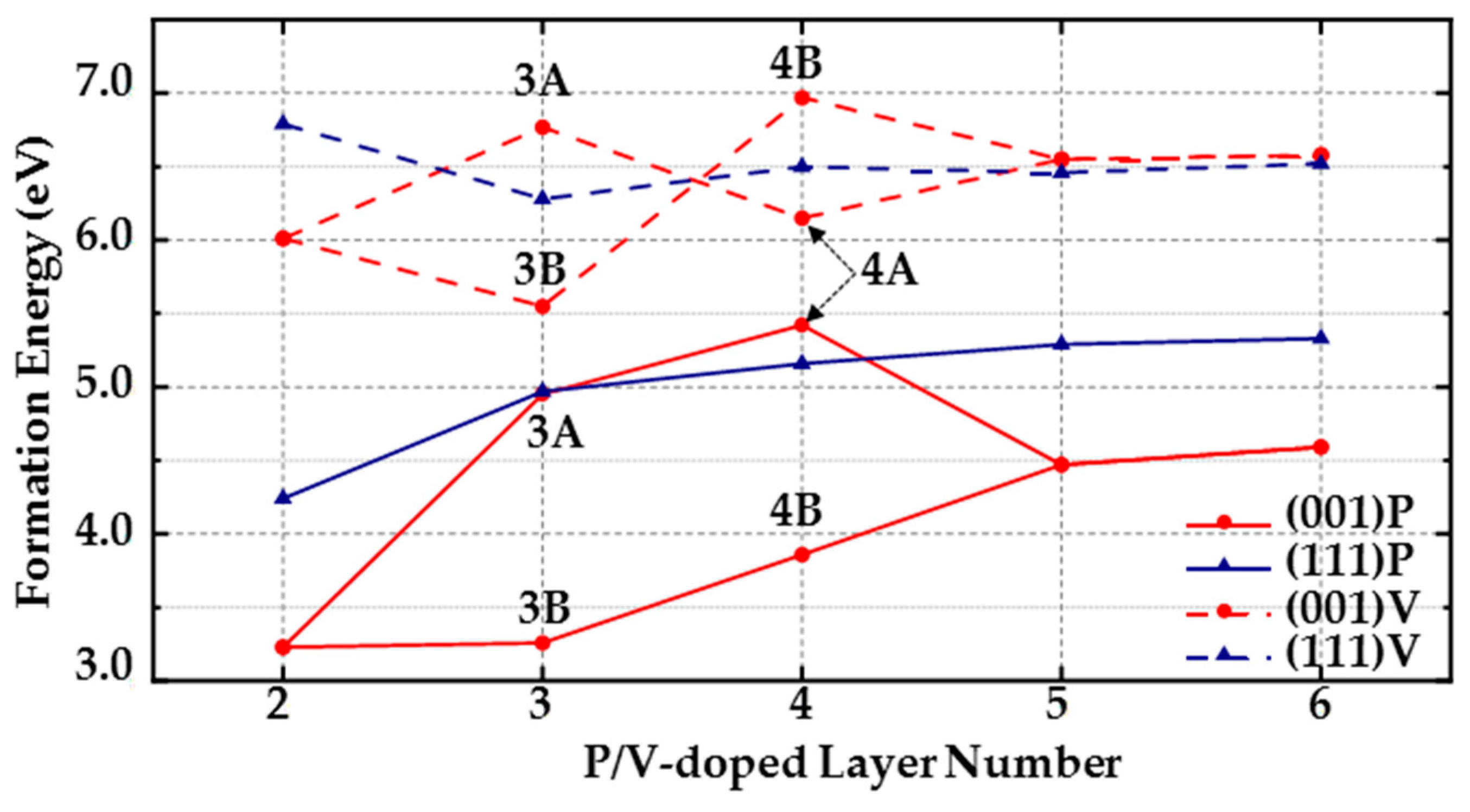
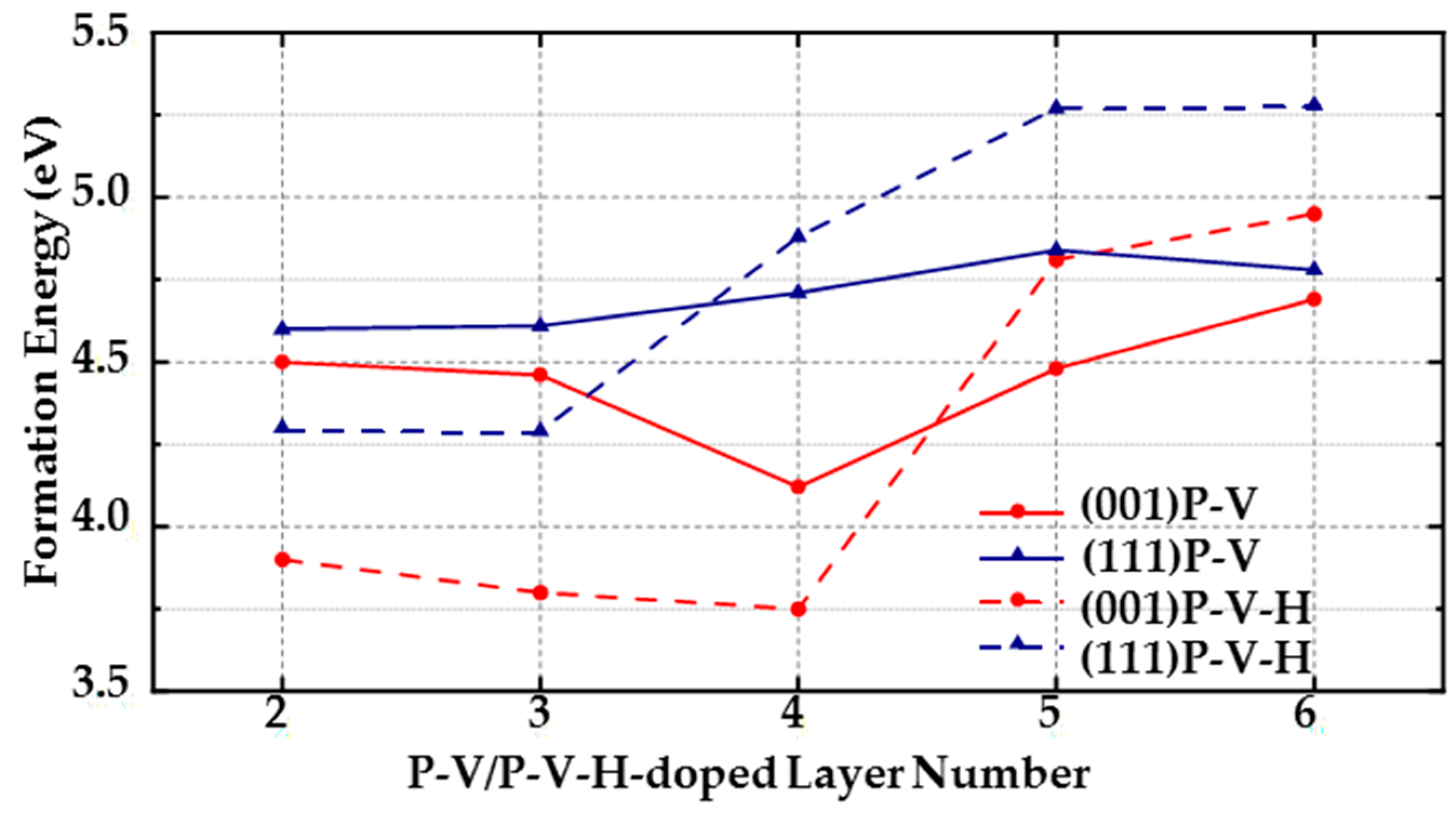
(1) For (111) diamond surfaces, the formation energy of the PV complex is lower than the formation energy of a single P atom in the third, fourth, fifth, and sixth layers. In the third and fourth layers, the formation energy of a single P atom is even higher than that of the PVH complex, indicating that when doping P atoms on (111) surfaces, the doped P atoms are likely to form PV and PVH complexes with the surrounding vacancies and H atoms. Thus, it is very important to control the number of vacancies and H atoms around doped P atoms during MPCVD fabrication of (111) diamond surfaces.
(2) The formation energy of a single P atom is generally the lowest in (001) surfaces in the second to sixth layers, which means that compared with a single P atom, PV and PVH complexes are less likely to form on (001) surfaces (but PV and PVH complexes form more easily than on (111) surfaces because the lowest formation energies of PV and PVH complexes in each layer of (001) surfaces are all lower than those of (111) surface. The lowest formation energy of doping a P atom in each layer of (001) surface is at least 0.74 eV lower than that of (111) surface). However, in the third and fourth layers, the formation energy of PVH complexes is close to or lower than the formation energy of doping a single P atom. For example, the lowest formation energy of PVH complexes in the fourth layer is 3.75 eV, and the lowest formation energy of doping a P atom in the fourth layer is 3.86 eV. Thus, decreasing the amount of hydrogen in the formation process of (001) diamonds can effectively reduce defects.
(3) Dopants cause surface structural deformation, and the formation energy is partly related to the extent of deformation. When the structural deformation is insufficient, distortions caused by doping are limited and eventually increase the formation energy, similar to doping a single P atom. When the structural deformation is excessive, more energy is required to reconstruct the surrounding structures, similar to the PV and PVH complexes.
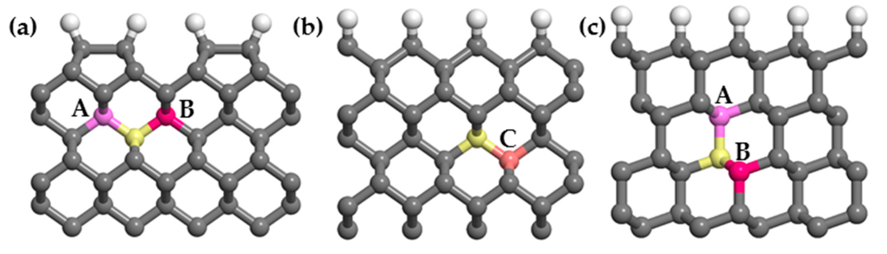
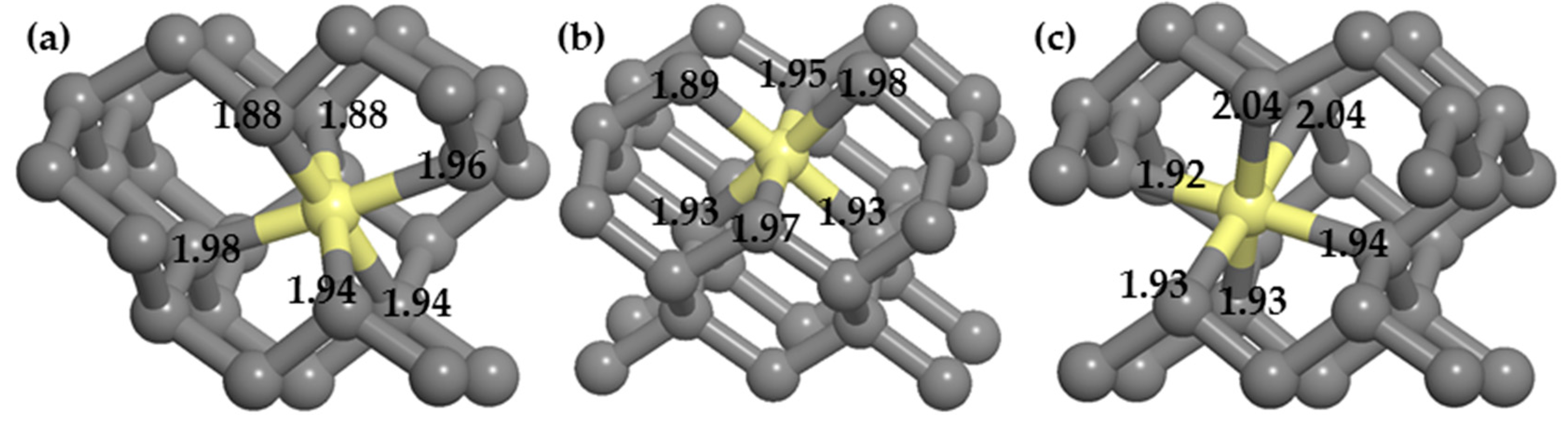
(4) Around the PVH complex, the P atom does not bond with the H atom, but instead bonds with the five nearby carbon atoms. Since phosphorus has only five valence electrons, compared with the six C–P bonds around PV complexes, the P–C bond populations around PVH complexes are higher, indicating that the P–C bonds around PVH complexes are stronger than those around PV complexes and P–C complexes are more stable than PV complexes.

Author Contributions

S.N. and W.S. contributed equally to this work. Conceptualization, S.S. and H.L.; methodology, S.N., W.S. and Y.P.; validation, S.N. and W.S.; formal analysis, S.N., W.S. and Y.S.; investigation, S.N. and W.S.; resources, S.S. and H.L.; data curation, S.N.; writing—original draft preparation, S.N.; writing—review and editing, Y.C. and H.Q.; visualization, S.N. and W.S.; su-pervision, S.S. and H.L.; project administration, H.L.; funding acquisition, W.S., S.S. and H.L. All authors have read and agreed to the published version of the manuscript.

Funding

This research was funded by the National Natural Science Foundation of China (No. 51727901), the China Scholarship Council (No. 201906270142), the International Cooperation Research Project of Shenzhen (No. GJHZ20180413182004161), the Hubei Provincial Natural Science Foundation of China under Grant (No. 2020CFA032) and the Guangdong Basic and Applied Basic Research Fund: Guangdong-Shenzhen Joint Fund (No. 2020B1515120005).

Data Availability Statement

The data used to support the findings of this study are available from the corresponding authors upon request.

Conflicts of Interest

The authors declare no conflict of interest.

References

  1. Kalish, R. Diamond as a unique high-tech electronic material: Difficulties and prospects. J. Phys. D Appl. Phys. 2007, 40, 6467–6478. [Google Scholar] [CrossRef]
  2. Kasu, M. Diamond epitaxy: Basics and applications. Prog. Cryst. Growth Charact. Mater. 2016, 62, 317–328. [Google Scholar] [CrossRef]
  3. Thiering, G.; Gali, A. Ab initio magneto-optical spectrum of Group-IV vacancy color centers in diamond. Phys. Rev. X 2018, 8, 1–17. [Google Scholar] [CrossRef] [Green Version]
  4. Pinault-Thaury, M.A.; Tillocher, T.; Habka, N.; Kobor, D.; Jomard, F.; Chevallier, J.; Barjon, J. N-type CVD diamond: Epitaxy and doping. Mater. Sci. Eng. B Solid State Mater. Adv. Technol. 2011, 176, 1401–1408. [Google Scholar] [CrossRef]
  5. Kato, H.; Takeuchi, D.; Tokuda, N.; Umezawa, H.; Yamasaki, S.; Okushi, H. Electrical activity of doped phosphorus atoms in (001) n-type diamond. Phys. Status Solidi Appl. Mater. Sci. 2008, 205, 2195–2199. [Google Scholar] [CrossRef]
  6. Wang, G.; Shao, Q. Electronic structures of phosphorus-doped diamond films and impacts of their vacancies. Sci. China Phys. Mech. Astron. 2010, 53, 1248–1254. [Google Scholar] [CrossRef]
  7. Haubner, R. Comparison of sulfur, boron, nitrogen and phosphorus additions during low-pressure diamond deposition. Diam. Relat. Mater. 2005, 14, 355–363. [Google Scholar] [CrossRef]
  8. Kajihara, S.A.; Antonelli, A.; Bernholc, J.; Car, R. Nitrogen and potential n-type dopants in diamond. Phys. Rev. Lett. 1991, 66, 2010–2013. [Google Scholar] [CrossRef] [PubMed]
  9. Miyazaki, T.; Okushi, H. A theoretical study of a sulfur impurity in diamond. Diam. Relat. Mater. 2001, 10, 449–452. [Google Scholar] [CrossRef]
  10. Karin, L. The Effect of Dopants on Diamond Surface Properties and Growth. Novel Aspects of Diamond, 2nd ed.; Yang, N., Ed.; Springer: Cham, Switzerland, 2015; pp. 31–53. [Google Scholar]
  11. Koizumi, S.; Kamo, M.; Sato, Y.; Ozaki, H.; Inuzuka, T. Growth and characterization of phosphorous doped {111} homoepitaxial diamond thin films. Appl. Phys. Lett. 1997, 71, 1065–1067. [Google Scholar] [CrossRef]
  12. Saito, T.; Kameta, M.; Kusakabe, K.; Morooka, S.; Maeda, H.; Hayashi, Y.; Asano, T.; Kawahara, A. Morphology and semiconducting properties of homoepitaxially grown phosphorus-doped (1 0 0) and (1 1 1) diamond films by microwave plasma-assisted chemical vapor deposition using triethylphosphine as a dopant source. J. Cryst. Growth. 1998, 191, 723–733. [Google Scholar] [CrossRef]
  13. Koizumi, S. Growth and characterization of phosphorus doped n-type diamond thin films. Phys. Status Solidi Appl. Res. 1999, 172, 71–78. [Google Scholar] [CrossRef]
  14. Nishitani-Gamo, M.; Yasu, E.; Xiao, C.; Kikuchi, Y.; Ushizawa, K.; Sakaguchi, I.; Suzuki, T.; Ando, T. Sulfur-doped homoepitaxial (001) diamond with n-type semiconductive properties. Diam. Relat. Mater. 2000, 9, 941–947. [Google Scholar] [CrossRef]
  15. Dannefaer, S.; Zhu, W. Vacancies in polycrystalline diamond films. Phys. Rev. B Condens. Matter Mater. Phys. 1996, 53, 1979–1984. [Google Scholar] [CrossRef]
  16. Czelej, K.; Zemła, M.R.; Kamińska, P.; Śpiewak, P.; Kurzydłowski, K.J. Clustering of hydrogen, phosphorus, and vacancies in diamond: A density functional theory analysis. Phys. Rev. B. 2018, 98, 1–13. [Google Scholar] [CrossRef]
  17. Shen, W.; Shen, S.; Liu, S.; Li, H.; Nie, S.; Pan, Y.; Tian, Z.; Li, Q. Binding of hydrogen to phosphorus dopant in phosphorus-doped diamond surfaces: A density functional theory study. Appl. Surf. Sci. 2019, 471, 309–317. [Google Scholar] [CrossRef]
  18. Kato, H.; Yamasaki, S.; Okushi, H. N-type doping of (001)-oriented single-crystalline diamond by phosphorus. Appl. Phys. Lett. 2005, 86, 1–3. [Google Scholar] [CrossRef]
  19. Miyazaki, T.; Kato, H.; Okushi, H.; Yamasaki, S. Ab initio energetics of phosphorus impurity in subsurface regions of hydrogenated diamond surfaces. E J. Surf. Sci. Nanotechnol. 2006, 4, 124–128. [Google Scholar] [CrossRef] [Green Version]
  20. Yan, C.X.; Dai, Y.; Guo, M.; Huang, B.B.; Liu, D.H. Theoretical characterization of carrier compensation in P-doped diamond. Appl. Surf. Sci. 2009, 255, 3994–4000. [Google Scholar] [CrossRef]
  21. Balasubramaniam, Y.; Pobedinskas, P.; Janssens, S.D.; Sakr, G.; Jomard, F.; Turner, S.; Lu, Y.G.; Dexters, W.; Soltani, A.; Verbeeck, J.; et al. Thick homoepitaxial (110)-oriented phosphorus-doped n-type diamond. Appl. Phys. Lett. 2016, 109, 1–5. [Google Scholar] [CrossRef]
  22. Clark, S.J.; Segall, M.D.; Pickard, C.J.; Hasnip, P.J.; Probert, M.I.J.; Refson, K.; Payne, M.C. First principles methods using CASTEP. Zeitschrift fur Krist 2005, 220, 567–570. [Google Scholar] [CrossRef] [Green Version]
  23. Vanderbilt, D. Soft self-consistent pseudopotentials in a generalized eigenvalue formalism. Phys. Rev. B 1990, 41, 7892–7895. [Google Scholar] [CrossRef]
  24. Perdew, J.P.; Burke, K.; Ernzerhof, M. Generalized gradient approximation made simple. Phys. Rev. Lett. 1996, 77, 3865–3868. [Google Scholar] [CrossRef] [Green Version]
  25. Hendrik, J.M.; Pack, J.D. Special points for Brillouin-zone integration Monkhorst and Pack. Phys. Rev. B 1976, 13, 5188–5192. [Google Scholar]
  26. Vanpoucke, D.E.P.; Haenen, K. Revisiting the neutral C-vacancy in diamond: Localization of electrons through DFT+U. Diam. Relat. Mater. 2017, 79, 60–69. [Google Scholar] [CrossRef] [Green Version]
  27. Tang, L.; Yue, R.; Wang, Y. N-type B-S co-doping and S doping in diamond from first principles. Carbon 2018, 130, 458–465. [Google Scholar] [CrossRef]
  28. Freysoldt, C.; Grabowski, B.; Hickel, T.; Neugebauer, J.; Kresse, G.; Janotti, A.; Van De Walle, C.G. First-principles calculations for point defects in solids. Rev. Mod. Phys. 2014, 86, 253–305. [Google Scholar] [CrossRef]
  29. Vanpoucke, D.E.P.; Nicley, S.S.; Raymakers, J.; Maes, W.; Haenen, K. Can europium atoms form luminescent centres in diamond: A combined theoretical–experimental study. Diam. Relat. Mater. 2019, 94, 233–241. [Google Scholar] [CrossRef] [Green Version]
  30. Kato, H.; Makino, T.; Yamasaki, S.; Okushi, H. N-type diamond growth by phosphorus doping on (0 0 1)-oriented surface. J. Phys. D Appl. Phys. 2007, 40, 6189–6200. [Google Scholar] [CrossRef]
  31. Nishimatsu, T.; Katayama-Yoshida, H.; Orita, N. Theoretical study of hydrogen-related complexes in diamond for low-resistive n-type diamond semiconductor. Phys. B Condens. Matter. 2001, 302–303, 149–154. [Google Scholar] [CrossRef]
  32. Robert, S.M. Electronic population analysis on LCAO-MO molecular wave functions. J. Chem. Phys. 1955, 23, 1833. [Google Scholar]
  33. Hirshfeld, F.L. Bonded-atom fragments for describing molecular charge densities. Theor. Chim. Acta. 1977, 44, 129–138. [Google Scholar] [CrossRef]
Figure 1. Schematic of the substitutional locations of the P and V on the (001) and (111) surfaces. (a) The doping location of P(V) on the (001) surface. (b) The doping location of P(V) on the (111) surface (white: H; gray: C; pink, blue, green, orange, red, yellow, and purple: P(V) in the site 2A, 3A, 3B, 4A, 4B, 5A, and 6A, respectively) the bottom two layers, framed by the red dotted line, are the atoms that are fixed during the calculation.
Applsci 11 01896 g001
Figure 2. Formation energies of the single V and single P atom doped in (001) and (111) surfaces. (The doped positions are illustrated in Figure 1).
Applsci 11 01896 g002
Figure 3. The possible vacancy locations around the doped P atom at the site 5A. (a) front view of the (001) surface, (b) side view of the (001) surface and (c) front view of the (111) surface (white: H; gray: C; yellow: P, purple, fuchsia and pink: V in the site A, B, and C, respectively).
Applsci 11 01896 g003
Figure 4. The optimized structures of PV complex when P (yellow) is in the site 5A on the (001) surface. (ac) represent V in the site A, B and C, respectively, the number in the figure represents the length of P–C bonds.
Applsci 11 01896 g004
Figure 5. The possible H sites around a PV complex.
Applsci 11 01896 g005
Figure 6. The lowest formation energies of PV and PVH complexes in each layer in (001) and (111) surface.
Applsci 11 01896 g006
Table 1. Calculation and lattice parameters of the two slab models.
SurfaceNumber of Carbon Layer (n)k Points SetCutoff Energy (eV)Size (x × y × z) (Å3)
(001)142 × 2 × 140010.06 × 10.06 × 23.27
(111)122 × 2 × 14007.55 × 8.71 × 23.06
Table 2. Change of typical bond lengths of a single P atom with its surrounding C atoms. The result of changing in bond length comes from: (length after doping−length before doping)/ length before doping.
SurfaceLayerPosition of PChange in Bond Length (%)
d1d2d3d4
(001)2A14.424.213.513.5
3A10.910.910.710.7
B9.59.510.510.5
4A10.09.59.89.8
B9.59.59.69.6
5A10.28.89.79.7
6A9.49.69.59.5
(111)2A14.411.010.610.6
3A11.59.89.99.9
4A10.29.39.39.3
5A10.09.99.59.5
6A10.19.79.49.4
Table 3. Change of typical bond lengths of PV complexes with the lowest formation energy in each layer with the surrounding C atoms. (+) indicates an increase in the bond length compared with the non-doped surface and (−) indicates a decrease in the bond length compared with the non-doped surface.
SurfaceLayerPosition of PPosition of VChange in Bond Length (%)
d1d2d3d4d5d6
(001)2AB20.520.627.4−18.1−23.8−23.8
3BB21.921.924.3−22.1−18.6−18.6
4AA22.822.825.8−22.3−22.3−18.8
5AA25.426.026.0−23.8−23.8−22.1
6AC25.325.327.2−23.0−22.8−22.4
(111)2AA23.923.924.7−24.0−24.1−24.0
3AA24.524.524.4−24.2−24.2−23.6
4AB25.527.625.7−22.3−21.0−22.1
5AB28.326.525.3−23.1−21.7−22.8
6AB26.428.225.5−23.2−21.5−22.5
Table 4. Change of typical bond lengths of PVH complexes with the lowest formation energy in each layer.
SurfaceLayerPosition of PPosition of VPosition of HBond Length (Å)Change in Bond Length (%)
P–HH–CP–C
(001)2ABBC12.2721.0831.421.2−29.5−26.4−20.7
3BBBC11.9391.0828.727.5−30.1−26.6−24.6
4BABC31.8971.0915.321.722.3−19.4−20.3
5AAAB21.6481.0613.120.620.6−20.6−20.6
6ACV1.6361.0722.120.814.0−19.8−19.9
(111)2AABC12.4401.0726.525.4−27.0−30.1−26.9
3AABC32.2481.0719.819.614.5−22.7−23.2
4ABAB31.6781.0820.922.314.6−19.8−21.0
5ABBC31.6491.0732.4−25.930.9−30.0−25.3
6ABAB21.6311.0721.522.113.5−19.0−19.3
Table 5. Atomic charges and electron bond population of the single P with its surrounding C atoms.
SurfaceLayerImpurity PositionP–C Bond PopulationP Atomic Charge (e)
(001)2A0.580.580.460.510.24
3A0.830.830.790.790.31
B0.830.800.820.820.35
4A0.860.860.830.830.32
B0.800.800.840.850.34
5A0.820.840.840.840.33
6A0.830.840.840.850.33
(111)2A0.810.810.810.820.36
3A0.820.820.830.84c0.34
4A0.850.850.850.820.33
5A0.820.820.830.850.33
6A0.830.830.830.840.33
Table 6. Atomic charges and electron bond population of the PV complex with the lowest formation energy in each layer.
SurfaceLayerPosition of PPosition of VP–C Bond PopulationP Atomic Charge (e)
(001)2AB0.470.470.380.550.550.550.22
3BB0.570.570.590.570.430.430.25
4AA0.570.570.550.550.550.430.22
5AA0.600.600.530.530.560.520.22
6AC0.530.570.560.550.550.530.23
(111)2AA0.580.580.560.530.530.530.23
3AA0.580.580.560.530.530.530.23
4AB0.540.580.530.570.510.500.23
5AB0.580.580.540.540.510.500.23
6AB0.580.580.540.540.510.510.23
Table 7. Atomic charges and electron bond population of the PVH complex with the lowest formation energy in each layer.
SurfaceLayerPosition of PPosition of VPosition of HBond Population of Charge (e) of
P–HH–CP–CPH
(001)2ABBC1−0.070.900.760.620.510.550.570.270.03
3BBBC1−0.120.980.710.590.650.660.530.280.01
4BABC3−0.120.980.710.590.650.650.530.280.01
5AAAB2−0.091.060.700.650.650.600.650.27−0.01
6ACV−0.081.050.690.650.640.650.610.27−0.00
(111)2AABC1−0.131.060.750.610.610.650.640.280.01
3AABC3−0.131.060.750.610.610.650.640.280.01
4ABAB3−0.050.970.710.640.620.610.590.27−0.00
5ABBC3−0.081.040.690.640.630.620.590.27−0.00
6ABAB2−0.071.040.680.640.650.630.600.27−0.00
Publisher’s Note: MDPI stays neutral with regard to jurisdictional claims in published maps and institutional affiliations.

