Article

Alternative Design of Binary Phase Diffractive Optical Element with Non-π Phase Difference

1
University of Electronic Science and Technology of China, Chengdu 610041, China
2
Institute of Optics and Electronics, Chinese Academy of Sciences, Chengdu 610209, China
*
Author to whom correspondence should be addressed.
Appl. Sci. 2021, 11(3), 1116; https://doi.org/10.3390/app11031116
Submission received: 6 January 2021 / Revised: 22 January 2021 / Accepted: 24 January 2021 / Published: 26 January 2021
(This article belongs to the Section Optics and Lasers)

Abstract

:

Featured Application

This work can be used to design the binary phase diffractive optical element for beam splitting with high diffraction efficiency and adjustable zero-order intensity.

Abstract

It was found that binary phase diffractive optical element (DOE) with non-π phase difference had higher diffraction efficiency and adjustable zero-order intensity than a 0-π one. However, existing design methods are all based on the simulated annealing algorithm and thus computationally expensive. In this paper, a simple and efficient method using the iterative Fourier transform algorithm (IFTA) is proposed. In this method, the target pattern is first modified via reducing the zero-order intensity. Then, the IFTA is adopted to design the conventional 0-π DOE. Subsequently, the phase distribution remains unchanged and the phase difference is carefully adjusted to increase the zero-order intensity so that the reconstructed pattern is consistent with the target. To verify this method, several typical DOEs for beam splitting were designed and fabricated, and the result showed that the proposed method is effective.

1. Introduction

In the past two decades, diffractive optical element (DOE) has received more and more attention due to its superior wavefront manipulation capability and unique advantages of high design flexibility, small size, and mass productivity. It expands the capabilities of conventional optics based on refraction or reflection and is now widely used in a broad range of applications, such as beam shaping [1,2,3], beam splitting [4,5,6], structured light projectors [7,8,9,10], pattern generation [11,12,13,14], optical security [15,16,17], and so on.
In general, the most commonly used method for fabrication of DOE is the lithographic technique adapted from the microelectronics industry. This approach can generate microstructures with up to 2n phase levels by using n binary masks. For DOE, the more the quantized phase levels, the higher the diffraction efficiency. However, multiple lithographic processing steps increase manufacturing cost and time and may introduce mask alignment errors that decrease element performance. In addition, minimum feature size and aspect ratio of the microstructures may also constrain the fabrication of a multilevel structure. Therefore, continuous phase profile of a DOE is usually quantized into binary phase levels (0, π) [18,19,20], which needs only one photolithography and no mask alignment.
In order to improve the efficiency of the binary phase DOE, Feldman et al. [21] considered the phase difference as a free parameter and then used the simulated annealing (SA) algorithm to optimize it together with the phase distribution. Diffraction efficiency of 74% can be obtained for the 3 × 3 array generator with phase step of 0.815π. In contrast, the efficiency of the conventional 0-π element is only 68%. However, it is not easy to find the optimal solution by optimizing the phase delay and distribution simultaneously. Subsequently, an improved approach was proposed by Hajj et al. [22]. The phase difference was fixed and then the SA algorithm was employed to find the best phase distribution. All possible values of the phase difference between 0 and π were explored. Although this method can find the optimal solution, the calculation process is very time-consuming because for each phase shift, one round of the SA algorithm is performed.
SA is a stochastic optimization algorithm [23]. To reach the global optimal solution, it needs to search enough time at each temperature. Therefore, the entire annealing process takes a lot of time. Compared with the SA algorithm, iterative Fourier transform algorithm (IFTA) [24], originally devised by Gerchberg and Saxton [25], is more efficient for the design of DOE, which has achieved considerable success in terms of less convergence time and clearer reconstruction. In this paper, a very simple and effective method based on the IFTA is presented to design the binary phase DOE with non-π phase difference. This method takes advantage of the special properties of the binary phase element and only needs to use the IFTA once. Compared with the existing methods based on the SA algorithm, design time can be greatly reduced while obtaining the same diffraction efficiency.

2. Method

Before giving the proposed design method, we first analyze the influence of phase difference change on the output light field for the conventional 0-π DOE. Figure 1a is the phase distribution of a binary DOE used to generate the 3 × 7 spot array with equal intensity. Figure 1b–d are the output light fields obtained by performing two-dimensional Fourier transform operation of the phase distribution in Figure 1a with phase difference of π, 0.9π, and 1.1π, respectively. The insets in the bottom are the cross-section intensity distribution. It can be seen that the reconstructed 3 × 7 spots are very uniform when phase difference is π. Then, when phase difference is changed to 0.9π or 1.1π, the spots are no longer uniform, which is mainly because the zero-order intensity is significantly enhanced compared to other diffraction orders. However, it should be noted that the uniformity of other diffraction orders except the zero order is still very good, which means that the change in phase difference does not affect the uniformity of other diffraction orders. The above analysis indicates that the 0-π DOE has the following interesting properties: when the phase difference is varied from π to other values, the zero-order light intensity will be enhanced, and the uniformity of other diffraction orders can be retained.
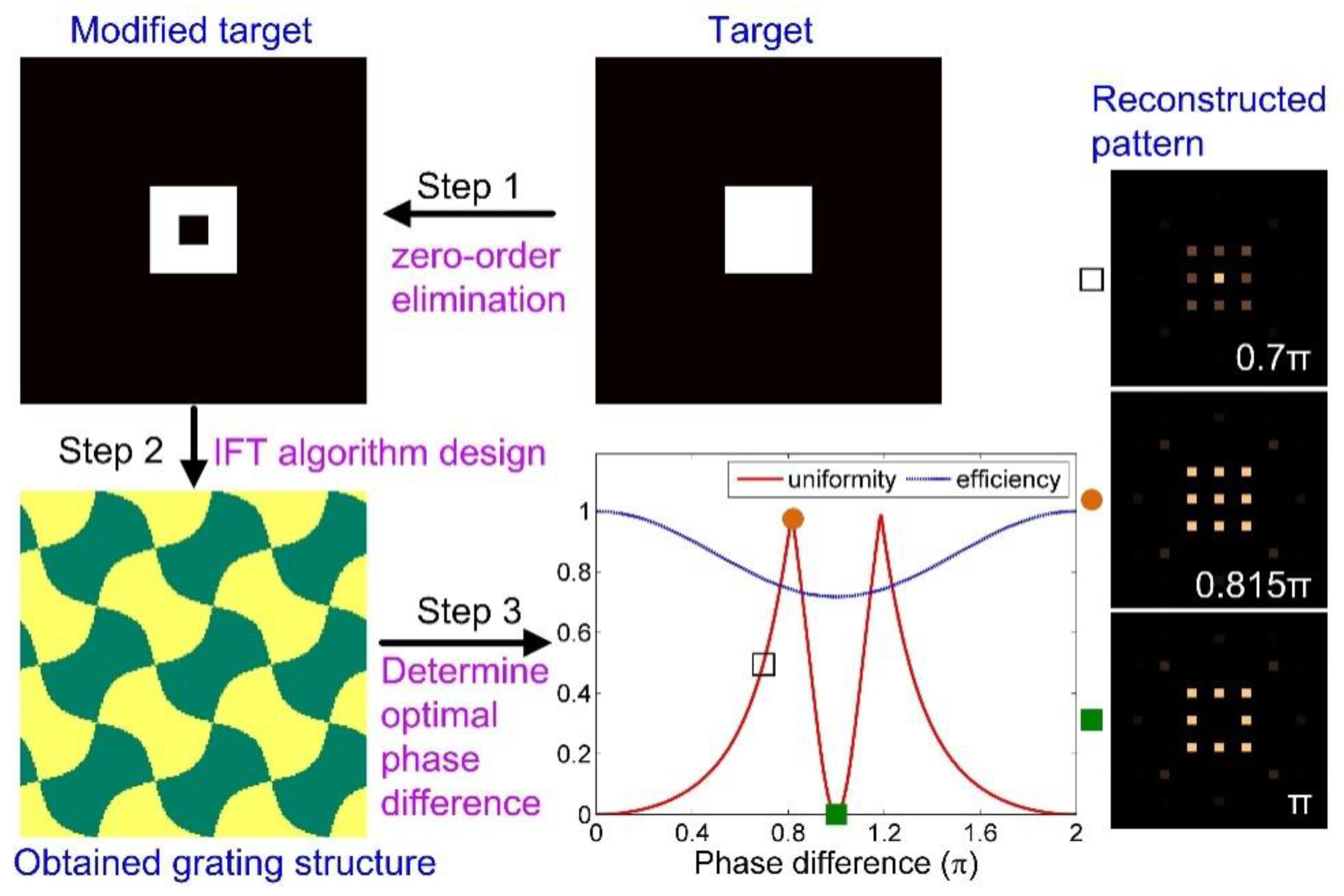
Our novel idea of the non 0-π DOE design is based on such special properties of the 0-π DOE. The detailed design process can be divided into three steps as shown in Figure 2. To begin with, the zero order of the target pattern is set to zero, resulting in a modified target pattern. Thereafter, the modified IFTA named three-step iterative soft quantization algorithm proposed by Wyrowski [26,27,28] is taken to design the 0-π DOE for this modified pattern. By iteratively applying the two-dimensional Fourier transform and inverse Fourier transform, and setting constrains at the DOE plane and output plane, the phase-only distribution can be obtained. In the DOE plane, the amplitude is removed and the phase is quantized progressively. In the output plane, the region of desired orders is defined as the signal window and the rest as the noise window. In the iteration, the complex amplitude in the noise area and the phase in the signal area are not constrained, which are referred to as amplitude freedom and phase freedom, respectively. Only the amplitude in the signal area is replaced by the target distribution multiplied by a scale factor, which is used to adjust the power repartition between the signal and noise areas. A more detailed flowchart can be found in [28]. When the iteration is terminated, phase distribution of the DOE can be obtained. As mentioned before, changing the phase difference of the 0-π DOE can enhance the zero-order intensity while maintaining the uniformity of other diffraction orders. Therefore, in the last step, we keep the phase distribution unchanged, then vary the phase difference from 0 to 2π, and calculate the corresponding output light field. For each value, the corresponding output light field is calculated with two-dimensional Fourier transform operation and the diffraction efficiency and uniformity are evaluated and plotted with respect to the phase difference. Finally, the optimal phase difference can be found intuitively from the curve. Diffraction efficiency η and uniformity σ are defined as follows:
η = I s / I ,
σ = 1 I s max I s min I s max + I s min ,
where Is and I denote the reconstructed intensity distribution in the desired diffraction orders and the whole output plane, respectively. Subscript max and min mean the maximum and minimum value.
A design example of a 3 × 3 beam splitter is also given in Figure 2. The lower left corner is the phase distribution of the 0-π DOE designed for the zero-order eliminated target pattern. The lower right corner shows the variation of the diffraction efficiency and uniformity with respect to the phase difference. The whole curve is symmetrically distributed because the symmetry of the Fourier transform for φ and 2π-φ phases. Thereby, it is only necessary to search for the optimal phase difference between 0 and π. It can be seen from the figure that as the phase difference decreases from π to zero, the uniformity first increases and then decreases. This is because when the phase difference deviates from π, the zero-order light intensity is gradually increased and consequently the uniformity gets better. Thereafter, as the phase difference is further reduced, zero-order intensity is gradually greater than other orders and therefore the uniformity is weakened. The reconstructed patterns corresponding to the phase difference of 0.7π, 0.815π, and π are also presented in Figure 2. The efficiency curve shows that the overall diffraction efficiency always increased with the phase difference decreases. This was mainly due to the increase in zero-order efficiency. Ultimately, when the phase difference was equal to 0.815π, the uniformity reached a maximum of 99% and the corresponding diffraction efficiency was 74%. This design result is comparable to the one in [22]. However, the proposed method only needs less than one minute of design time, while the original SA-based method needs several hours.

3. Simulation

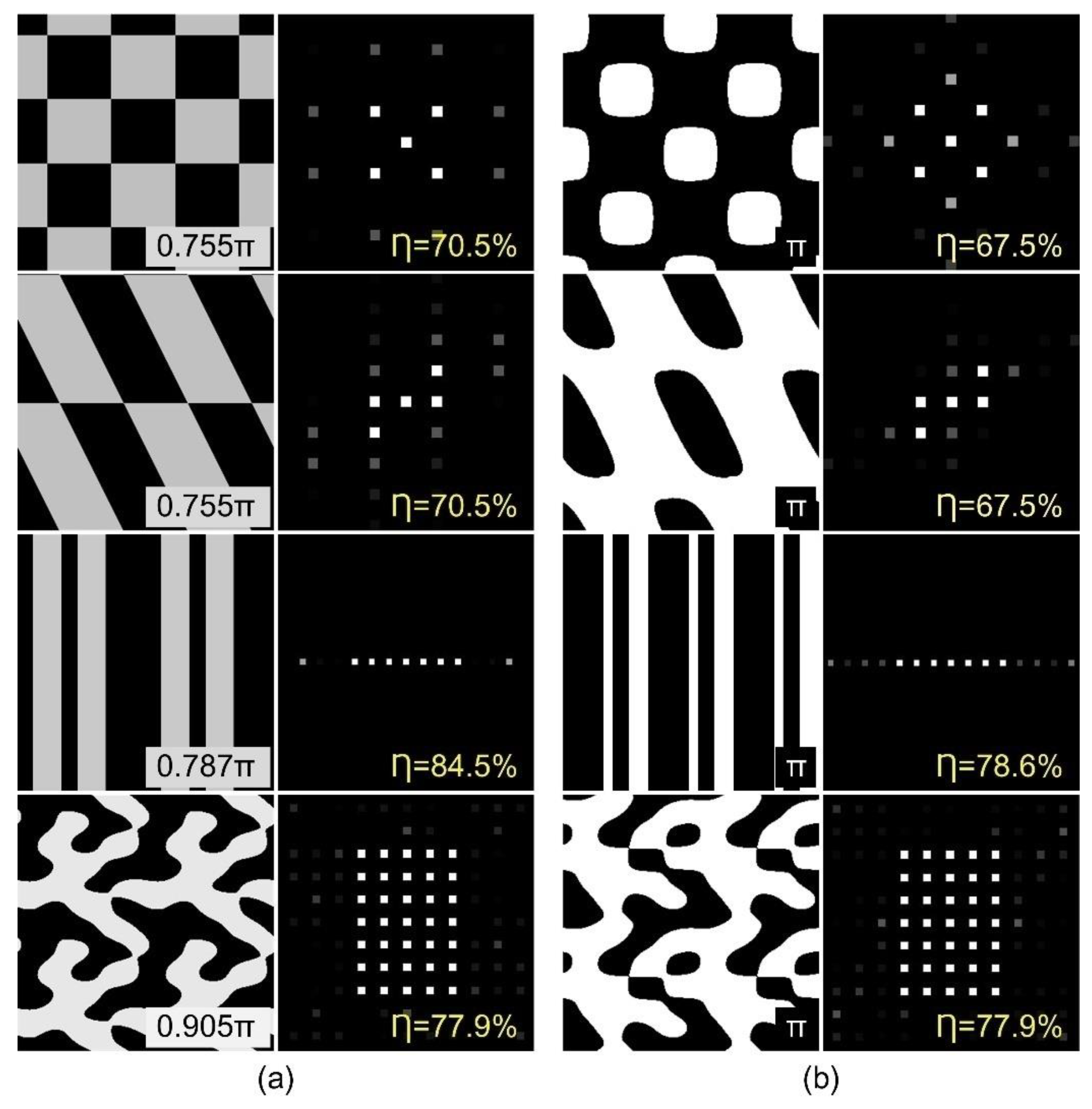
To further verify the effectiveness of the proposed method, a variety of DOEs were designed to generate different patterns. Figure 3 shows the design results of the DOEs for four patterns with the proposed non 0-π design method and the conventional 0-π design method. Due to the sensitivity of the iterative Fourier transform algorithm to the initial phase distribution, we performed 20 designs for each pattern and selected the best results. It should be pointed out that the uniformity of the reconstructed pattern obtained by both design methods were all above 98%and showed no significant difference, so it is not given in the figure. The achieved phase differences of the non 0-π DOEs were 0.755π, 0.755π, 0.787π, and 0.905π, respectively. The corresponding numerically reconstructed light fields indicated that the designed non 0-π DOEs were correct and could produce high-precision diffraction patterns. The calculated diffraction efficiencies were 70.5%, 70.5%, 84.5%, and 77.9%, respectively. For comparison, the obtained efficiencies of the traditional 0-π DOEs were 67.5%, 67.5%, 78.6%, and 77.9%, respectively. We can see that the diffraction efficiency of the non 0-π DOE was obviously higher than that of the 0-π DOE for the first three diffraction patterns. For the fourth 7 × 5 beam splitter design, however, the results were similar. This indicates that in some cases, the non-π DOE can indeed improve the diffraction efficiency, and in another cases, it cannot.
Although non 0-π DOE does not always get a higher diffraction efficiency, it has a special property [29]. That is, when the step height is less than the theoretical value, the zero-order intensity is greater than the other order. Conversely, when the step height is higher than the theoretical value, the zero-order intensity is less than that of other orders. Figure 4 shows the numerical reconstructed intensity distribution of the designed non 0-π DOE for 1 × 7 beam splitting at different etching depth. The optimal phase difference is 0.787π. Here we assumed that wavelength was λ = 650 nm, fused silica was used as the substrate with refractive index of n = 1.4565 at this wavelength. Thus, theoretical depth of the designed DOE was d = λφ/(2(n − 1)) = 560 nm. It can be seen that when the etching depth is lower than the theoretical depth, the zero-order light intensity will be greater than other orders. Conversely, the zero-order intensity will be smaller. In fact, this phenomenon was already confirmed by the result in Figure 2. The reason mainly lies in that when the phase difference moves close to π, the zero-order light intensity will always reduce for the binary-phase DOE. Therefore, when the phase difference is larger than the optimal value, meaning that the phase difference is closer to π, the zero order will be weaker. In contrast, when the phase difference is less than the optimal value, it means that the phase difference is farther from π, so the zero-order will be enhanced. This unique zero-order adjustable character is very useful in the fabrication process because we can judge whether the etching depth is smaller or larger than the target by comparing the intensity of the zero order with other orders, especially for DOEs with small feature size, where it is difficult to accurately measure the etching depth with step meter or white light interferometer. In contrast, zero-order intensity will always increase when the depth deviates from the target for the traditional 0-π DOE, as shown in Figure 5. The theoretical depth of this 0-π DOE was d = λ/(2(n − 1)) = 712 nm.
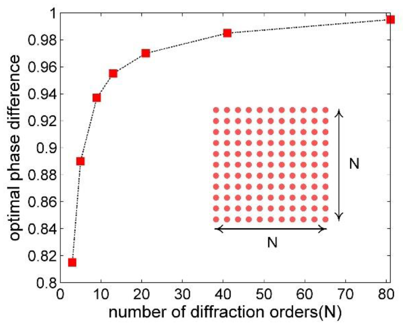
In Figure 3, we find that as the number of diffraction orders contained in the target pattern increased, the optimal phase difference moved toward π gradually. In order to verify this speculation, we chose the square pattern consisting of N × N orders as the target light field, as shown in the inset of Figure 6, and performed the non 0-π DOE design. The obtained optimal phase difference under different numbers of diffraction orders N is plotted in Figure 6. It can be seen that as N increased from 3 to 11, the optimal phase difference increased rapidly from 0.8π to 0.955π. Thereafter, with the increase of N, the optimal phase difference increased slowly. When N was equal to 81, the optimal phase difference reached 0.995π. From the variation law of the curve, we can conclude that when a target light field contains a small number of diffraction orders, a non 0-π DOE design can be considered to improve the diffraction efficiency. Conversely, when the target light field contains a large number of diffraction orders, it is recommended to design the traditional 0-π DOE.

4. Experiment

To further validate the proposed method, non 0-π DOEs for generating various diffraction orders distributions were fabricated and optically characterized. The lithography and reactive ion etching technique were adopted to create binary relief structures on the fused silica substrate. More detailed process flow can be found in [29]. Figure 7a shows the 2.5-inch mask and the fabricated two DOEs with etching depth of 550 and 661 nm. To simplify processing, eight phase distributions for the generation of eight different diffraction patterns were drawn on the same mask, represented by the number from 1 to 8 in the figure. Each had the same sampling interval of 1 × 1 μm, period of 129 × 129 μm, and total area of 1 × 1 cm. Figure 7b shows the optical configuration used to test the performance of the fabricated DOEs. A monochromatic laser with a wavelength of 650 nm irradiated the DOE vertically, thus forming a far-field diffraction pattern on the white screen, which was then captured by the Cannon camera. The attenuator was used to adjust the intensity of the laser.
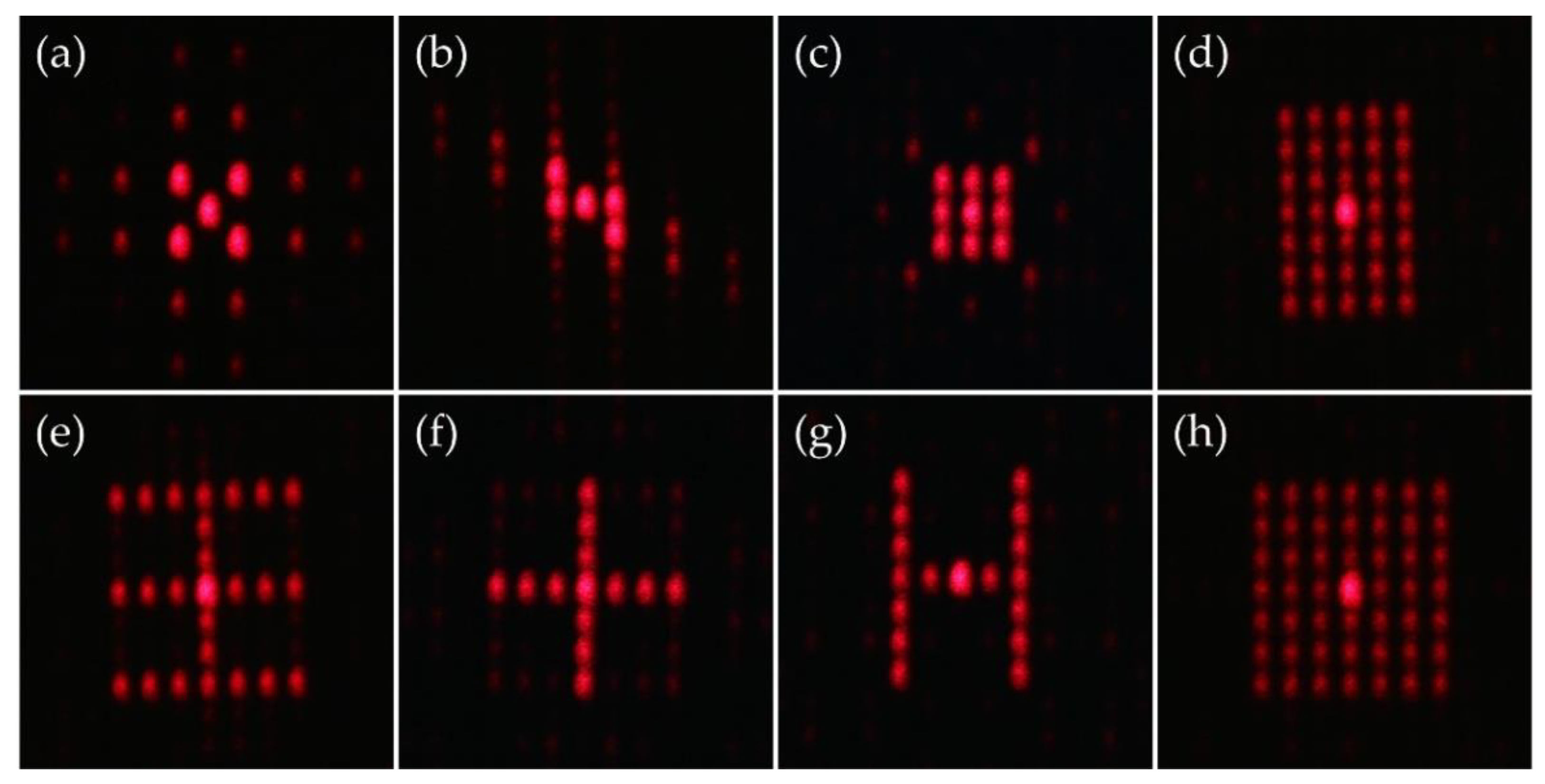
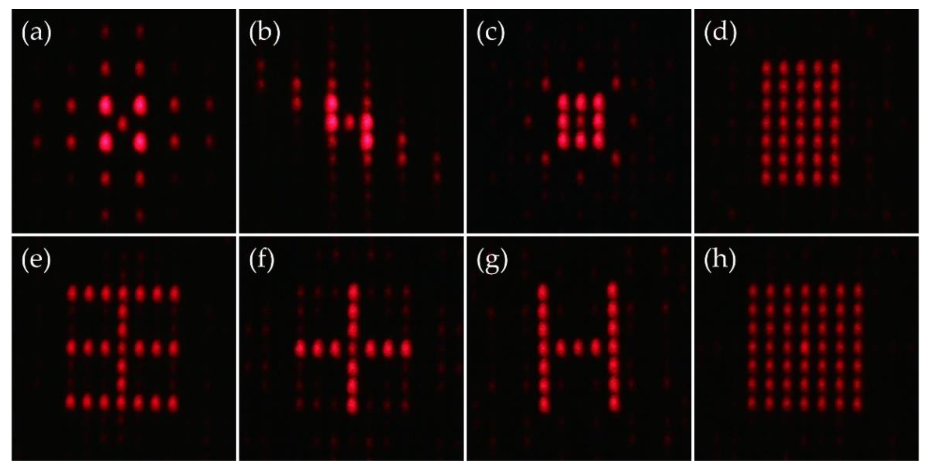
Figure 8 shows the captured diffraction patterns of the 1# DOE with etching depth of 550 nm. It can be seen that light intensity of the zero order in Figure 8a–c was similar to that of other orders and the patterns were well reconstructed. However, the zero order was significantly brighter than other orders in Figure 8d–h. This difference was due to the fact that for the eight target patterns, the optimal phase difference of the designed non 0-π DOEs were not equal, and are 0.755π, 0.755π, 0.815π, 0.905π, 0.889π, 0.854π, 0.87π, and 0.92π, respectively. For the binary phase DOE with phase difference φ, the theoretical etching depth was determined by d = λφ/(2(n − 1)). Here the refractive index of the fused silica was n = 1.4565 at the wavelength of λ = 650 nm. Then, the corresponding theoretical etching depths of the eight patterns were 537 nm, 537 nm, 580 nm, 644 nm, 633 nm, 608 nm, 619 nm, and 655 nm, respectively. Since the depth 550 nm of the 1# DOE was similar to the target values of the patterns in Figure 8a–c, the reconstructed light fields were uniform. While for the patterns in Figure 8d–h, the depth was smaller than the theoretical depth. Therefore, the zero-order was stronger than other orders. Figure 9 shows the captured diffraction patterns of the 2# DOE with etching depth of 661 nm. We can see that in this case the patterns in the Figure 8d–h were well reconstructed. For the patterns in Figure 9a–c, since the depth was much greater than the theoretical depth, the zero-order light was significantly weaker than the other orders. The experimental results are in good agreement with the numerical simulation, which showed that the proposed method is effective for non 0-π DOE design.

5. Conclusions

In this paper, a very simple and efficient method for the design of binary phase-only diffractive optical element with non-π phase difference was proposed. Compared with the existing design method based on simulated annealing algorithm, the proposed method needs to optimize the phase distribution of the DOE only once and subsequently with a simple search process of the optimal phase difference. Therefore, the design time is greatly shortened. Simultaneously, the simulation and experimental results show that the designed non 0-π DOEs can generate high-precision target light field. One thing should be pointed out that the proposed method is not general to every binary phase diffractive optical element, but it is limited to the application of creating a symmetric and equal intensity array of spots. Even so, we still believe that the proposed design method has great application prospects in the field of laser beam splitting, pattern generation, and so on.

Author Contributions

Conceptualization, C.X. and H.P.; methodology, C.X.; software, C.X. and A.C.; validation, C.X.; writing—original draft preparation, C.X.; writing—review and editing, H.P.; supervision, Q.D.; funding acquisition, H.P. All authors have read and agreed to the published version of the manuscript.

Funding

This research was funded by National Natural Science Foundation of China (NSFC) (61905251) and Applied Basic Research Programs of Department of Science and Technology of Sichuan Province (2019YJ0014).

Institutional Review Board Statement

Not applicable.

Informed Consent Statement

Not applicable.

Data Availability Statement

The data presented in this study are available on request from the corresponding author.

Conflicts of Interest

The authors declare no conflict of interests.

References

  1. Fernandez, J.M.H.; Brea, L.M.S.; Bernabeu, E. Near-field shaping with two binary diffractive optical elements in tandem. Opt. Commun. 2013, 297, 182–189. [Google Scholar] [CrossRef]
  2. Pang, H.; Liu, W.; Cao, A.; Deng, Q. Speckle-reduced holographic beam shaping with modified Gerchberg-Saxton algorithm. Opt. Commun. 2019, 433, 44–51. [Google Scholar] [CrossRef]
  3. Vasu, D.; Andra, R.; Vishwa, P. Generation of uniform-intensity light beams with controllable spatial shapes. Opt. Commun. 2020, 475, 126226. [Google Scholar]
  4. Mait, J.N. Design of binary-phase and multiphase Fourier gratings for array generation. J. Opt. Soc. Am. A 1990, 7, 1514–1528. [Google Scholar] [CrossRef]
  5. Zhou, C.; Liu, L. Numerical study of Dammann array illuminators. Appl. Opt. 1995, 34, 5961–5969. [Google Scholar] [CrossRef] [PubMed]
  6. Kim, D.; Keesling, A.; Omran, A.; Levine, H.; Bernien, H.; Greiner, M.; Lukin, M.; Englund, D. Large-scale uniform optical focus array generation with a phase spatial light modulator. Opt. Lett. 2019, 44, 3178–3181. [Google Scholar] [CrossRef] [PubMed]
  7. Barlev, O.; Golub, M.A. Multifunctional binary diffractive optical elements for structured light projectors. Opt. Express 2018, 26, 21092–21107. [Google Scholar] [CrossRef] [PubMed]
  8. Miao, Y.; Zhao, Y.; Ma, H.; Jiang, M.; Lin, J.; Jin, P. Design of diffractive optical element projector for a pseudorandom dot array by an improved encoding method. Appl. Opt. 2019, 58, G169–G176. [Google Scholar] [CrossRef] [PubMed]
  9. Kim, D.; Hermserschmidt, A.; Dyachenko, P.; Scharf, T. Inverse design and demonstration of high-performance wide-angle diffractive optical elements. Opt. Express 2020, 28, 22321–22333. [Google Scholar] [CrossRef] [PubMed]
  10. Gu, F.; Song, Z.; Zhao, Z. Single-shot structured light sensor for 3D dense and dynamic reconstruction. Sensors 2020, 20, 1094. [Google Scholar] [CrossRef] [PubMed] [Green Version]
  11. Pasienski, M.; DeMarco, B. A high-accuracy algorithm for designing arbitrary holographic atom traps. Opt. Express 2008, 16, 2176–2190. [Google Scholar] [CrossRef] [PubMed] [Green Version]
  12. Mohammad, N.; Meem, M.; Wan, X.; Menon, R. Full-color large are a transmissive holograms enabled by multi-level diffractive optics. Sci. Rep. 2017, 7, 5789. [Google Scholar] [CrossRef] [PubMed]
  13. Chen, L.; Zhang, H.; He, Z.; Wang, X.; Cao, L.; Jin, G. Weighted constraint iterative algorithm for phase hologram generation. Appl. Sci. 2020, 10, 3652. [Google Scholar] [CrossRef]
  14. Su, P.; Cai, C.; Song, Y.; Ma, J.; Tan, Q. A hybrid diffractive optical element design algorithm combining particle swarm optimization and a simulated annealing algorithm. Appl. Sci. 2020, 10, 5485. [Google Scholar] [CrossRef]
  15. Goncharsky, A.; Durlevich, S. High-resolution computer-generated hologram for creating 2D images with kinematic effects of motion. J. Opt. 2020, 22, 115702. [Google Scholar] [CrossRef]
  16. Wang, H.; Piestun, R. Azimuthal multiplexing 3D diffractive optics. Sci. Rep. 2020, 10, 6438. [Google Scholar] [CrossRef] [Green Version]
  17. Goncharsky, A.; Durlevich, S. DOE for the formation of the effect of switching between two images when an element is turned by 180 degrees. Sci. Rep. 2020, 10, 10606. [Google Scholar] [CrossRef]
  18. Wyrowski, F. Diffractive optical elements: Iterative calculation of quantized, blazed phase structures. J. Opt. Soc. Am. A 1990, 7, 961–969. [Google Scholar] [CrossRef]
  19. Liu, X.; Lv, G.; Ding, S.; Wang, Z.; Wang, S.; Feng, Q. Regional iterative optimization algorithm to reduce error caused by DOE binarization. Appl. Opt. 2019, 58, 7227–7232. [Google Scholar] [CrossRef]
  20. Wildi, T.; Kiss, M.; Quack, N. Diffractive optical elements in single crystal diamond. Opt. Lett. 2020, 45, 3458–3461. [Google Scholar] [CrossRef]
  21. Feldman, M.R.; Guest, C.C. Iterative encoding of high-efficiency holograms for generation of spot arrays. Opt. Lett. 1989, 14, 2023–2025. [Google Scholar] [CrossRef] [PubMed]
  22. Hajj, B.; Oudjedi, L.; Fiche, J.; Dahan, M.; Nollmann, M. Highly efficient multicolor multifocus microscopy by optimal design of diffraction binary gratings. Sci. Rep. 2017, 7, 5284. [Google Scholar] [CrossRef] [PubMed] [Green Version]
  23. Kirkpatrick, S.; Gelatt, C.D.; Vecchi, M.P. Optimization by simulated annealing. Science 1983, 220, 671–680. [Google Scholar] [CrossRef] [PubMed]
  24. Olivier, R.; Ville, K.; Hans, H. Review of iterative Fourier-transform algorithms for beam shaping applications. Opt. Eng. 2004, 43, 2549–2556. [Google Scholar]
  25. Gerchberg, R.W.; Saxton, W.O. A practical algorithm for the determination of phase from image and diffraction plane pictures. Optik 1972, 35, 237–246. [Google Scholar]
  26. Wyrowski, F.; Bryngdahl, O. Iterative Fourier-transform algorithm applied to computer holography. J. Opt. Soc. Am. A 1988, 5, 1058–1065. [Google Scholar] [CrossRef]
  27. Wyrowski, F. Iterative quantization of amplitude holograms. Appl. Opt. 1989, 28, 3864–3870. [Google Scholar] [CrossRef]
  28. Buhling, S.; Wyrowski, F. Improved transmission design algorithms by utilizing variable strength projections. J. Mod. Opt. 2002, 49, 1871–1892. [Google Scholar] [CrossRef]
  29. Pang, H.; Cao, A.; Liu, W.; Li, S.; Deng, Q. Alternative design of Dammann grating for beam splitting with adjustable zero-order light intensity. IEEE Photon. J. 2019, 11, 1500909. [Google Scholar] [CrossRef]
Figure 1. (a) Phase distribution of the calculated binary diffractive optical element (DOE) and the reconstructed intensity distribution with phase difference of (b) π, (c) 0.9π, (d) 1.1π.
Applsci 11 01116 g001
Figure 2. Schematic diagram of the proposed method.
Applsci 11 01116 g002
Figure 3. Calculated phase distributions and the reconstructed patterns: (a) proposed non 0-π design result, (b) conventional 0-π design result.
Applsci 11 01116 g003
Figure 4. Simulated reconstructed intensity distribution of the designed non 0-π DOE for 1 × 7 beam splitting with etching depth of (a) 530 nm; (b) 560 nm; (c) 590 nm.
Applsci 11 01116 g004
Figure 5. Simulated reconstructed intensity distribution of the traditional 0-π DOE for 1 × 7 beam splitting with etching depth of (a) 562 nm; (b) 712 nm; (c) 762 nm.
Applsci 11 01116 g005
Figure 6. The obtained optimal phase differences for the target patterns with different number of diffraction orders N.
Applsci 11 01116 g006
Figure 7. (a) mask and the fabricated DOEs; (b)Experimental test system.
Applsci 11 01116 g007
Figure 8. Diffraction pattern of the 1# DOE with etching depth of 550 nm. Theoretical depths of the eight patterns are (a) 537 nm, (b) 537 nm, (c) 580 nm, (d) 644 nm, (e) 633 nm, (f) 608 nm, (g) 619 nm, and (h) 655 nm.
Applsci 11 01116 g008
Figure 9. Diffraction pattern of the 2# DOE with etching depth of 661 nm. Theoretical depths of the eight patterns are (a) 537 nm, (b) 537 nm, (c) 580 nm, (d) 644 nm, (e) 633 nm, (f) 608 nm, (g) 619 nm, and (h) 655 nm.
Applsci 11 01116 g009
Publisher’s Note: MDPI stays neutral with regard to jurisdictional claims in published maps and institutional affiliations.