1. Introduction
The development in solid-state electronics is playing a major contribution to the development of modern society. However, the operation of these pieces of equipment is very sensitive to variation in the supplied voltage [
1,
2]. The main source of their incorrect outputs is the decrease and increase in values of the supplied voltage. In power quality terminology, this problem is regarded as voltage sag if the line rms voltage is reduced (80% to 20%) with respect to nominal rated rms values during some input voltage cycles [
3]. This situation requires the addition of voltage in the line that may achieve with the non-inverted output of the voltage stabilizers. The other type of voltage variation is characterized as voltage swell in which the line rms voltage is boosted to 110% to 180% of its normal rated value for a few milliseconds [
4]. The correction of this situation requires injecting the voltage of opposite polarity of the line that can obtain from the inverted output of the voltage controllers. These problems are very frequent and challenging in power distribution systems during fault conditions [
5,
6]. For example, once there is a line-to-ground fault, the faulty line faces voltage sag while other phases experience a voltage swell problem. They may be resolved by adding and subtracting the voltage generated by the voltage controllers. The magnitude of the correcting voltage may be less than the voltage of the faulty phase if the depth level of the voltage variation is less than 50%, which requires the voltage buck characteristics of the generated voltage. On the other side, it requires the voltage boost feature if the required level of the correcting voltage is more than 50%. Therefore, voltage buck and boost features with dual polarities are a mandatory requirement of the correcting voltage for any depth level problem.
The traditional way to resolve these issues is the use of indirect approaches of AC-AC conversion [
7,
8,
9,
10]. That requires power conversion in two stages where a DC-link capacitor is a mandatory requirement between the two converters. Here at the front stage, a low-frequency rectifier circuit transforms AC power to DC power to store in a DC-link capacitor. This stage may be a controlled rectifier if regulation of voltage at the DC-link level is required. This control highly decreases the power quality of input current that can only be tackled using harmonic suppression filters or complex switching arrangements. The second converting stage is responsible for DC to AC conversion, and once again, a complex control arrangement is required to tackle the low power quality. The other approach to address and tackle the low power quality issues is the execution of power conversion in multistage [
8] or multilevel configuration [
9,
10]. This overall arrangement is complicated to realize, and DC-link capacitors are a big source of poor system reliability [
11]. This approach is not feasible or smart for applications where only voltage control is essential at source frequency.
The direct AC-AC conversion is a smart solution for stabilizing the line voltage as it is realized without a DC-link capacitor. This solution approach is simple, less complex, and implementable in a single stage. So, it gains more attention from the researchers and developers. Thyristor-based AC voltage controllers (on-off or phase-angle) have some potency for low power application as the generated harmonics are always low frequency and have very severe power quality-related issues [
12]. AC voltage controller based on high-frequency pulse-width modulation (PWM) control can be employed to tackle the low power quality concerns but their voltage gain is low (less than one) with unipolar capabilities. The voltage stabilization characteristics in direct AC-AC converters may be realized with the similar approach as adopted in direct DC-DC converters just with the replacement of unidirectional operating semiconductor devices with bidirectional devices as proposed in [
13]. The converters based on this approach mentioned in [
1,
13] have positive or negative voltage gain, so they can only address either voltage sag or swell issue.
The direct AC-AC converters reported in [
14,
15,
16] use a z-source structure to ensure the dual polarity voltage. This structure also facilitates tackling the shoot-through challenge of the complementary operated switching devices. Z-source structure is a specific arrangement of many inductors and capacitors that not only result in large size or cost but also it is a big source of slow system’s dynamic behavior. The deficiencies resulting from these power converting approaches are tackled with other AC-AC techniques applied in non-z-source structures as reported in [
17,
18,
19,
20]. The converter employed with the structure reported in [
3] has bipolar voltage buck characteristics, and its application is only limited to the compensation of the low depth level power quality issues. Conversely, the voltage controllers as applied in [
4] have only voltage boosting features. It can only tackle the power quality problem where the voltage correcting level is more than 50%. These stated voltage controllers lack the compensation for all depth level problems required for reliable operation in the power system.
Voltage buck and boost operation ensure the generation of correcting voltage for any depth level problem. Such voltage compensating techniques are addressed in [
19,
20]. The power converters, as stated in [
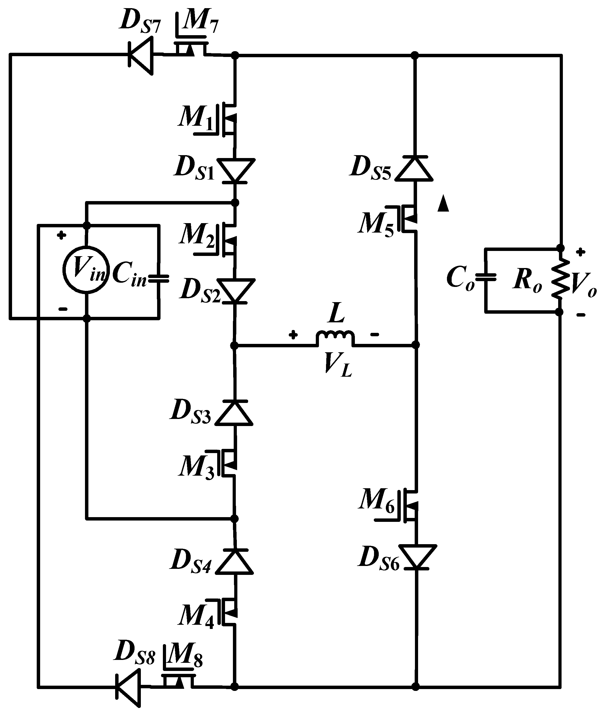
19], can generate correcting voltage with any polarity but its operation is only limited to voltage buck-boost capabilities. This circuit has many serious power quality concerns, such as a high ripple in the inductor current and output capacitor voltage. Furthermore, a high value of operating current and break-over voltage is the main source of high losses. It also increases the power rating of solid-state devices. The buck and boost operation rather than buck-boost can be employed to address these concerns. One of such approaches as illustrated in
Figure 1 is stated in [
20]. The realization of this approach requires the use of eight high switching diodes and eight metal-oxide field-effect transistors (MOSFETs). Each diode and MOSFET form a pair that converts the bidirectional current conduction characteristics of a MOSFET into unidirectional. These current conduction capabilities block the conduction of the MOSFET’s body diode that has very slow reverse characteristics. This arrangement also ensures the elimination of the shoot-through issue that avoids the current interruption of the inductor. The main issue of such topology is the use of a large number of diodes and especially transistors. The on and off control of a transistor is a big challenge, especially once it is connected to a high voltage side (a situation in which the reference terminal of the transistor is not connected to the reference point of the circuit). Switching of transistors (MOSFETs) in such circumstances requires the use of a reliable gate supporting circuit. This circuit may be implemented with a number of passive components, microelectronic devices, and separate isolated DC sources. This arrangement increases the volume and cost of the overall system as the size of the gate operating circuit is always much larger than the operating transistor. There are also some associated control circuit losses as addressed in [
21,
22].
In keeping these constraints, we have eliminated the use of two diodes and two transistors in our newly developed power converting approach that can generate the same outputs as obtained in [
20]. The reduction of two transistors compacts the size of the converter as there is the elimination of two gate operating circuits and two separate isolated DC sources. This overall arrangement lowers the size, cost, and losses of the system.
The rest of the arrangement of this article includes the introduction of the proposed topology and its operating modes in
Section 2. Here the relation of output voltage to the input voltage is correlated with the help of inductor voltage. The conversion losses are discussed in
Section 2.
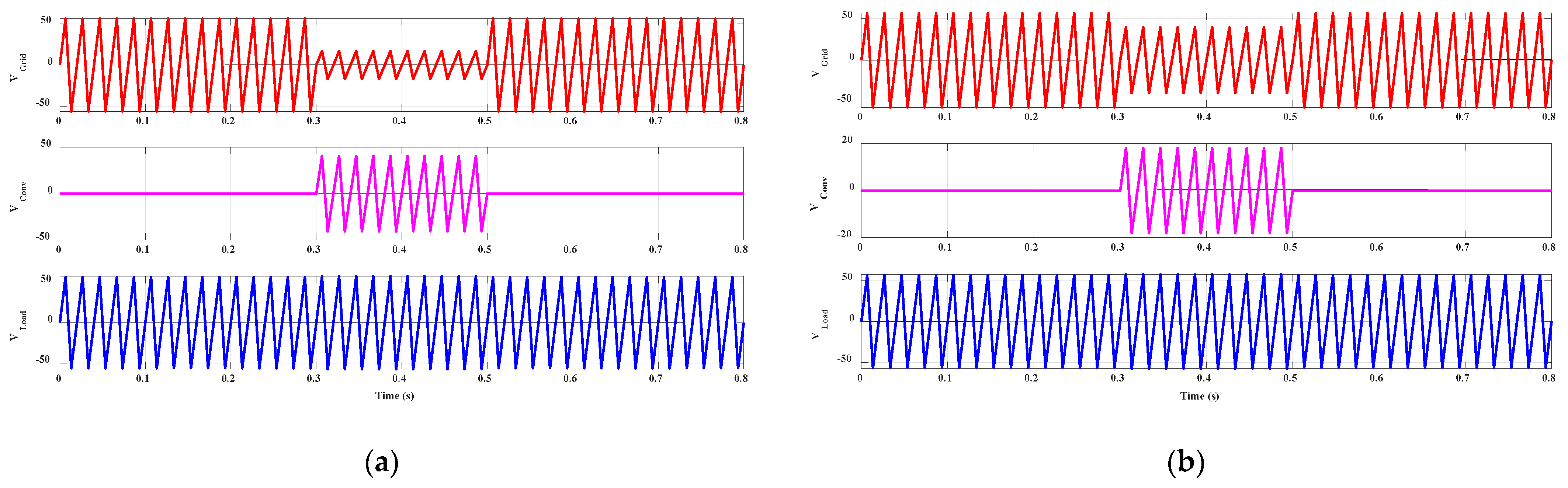
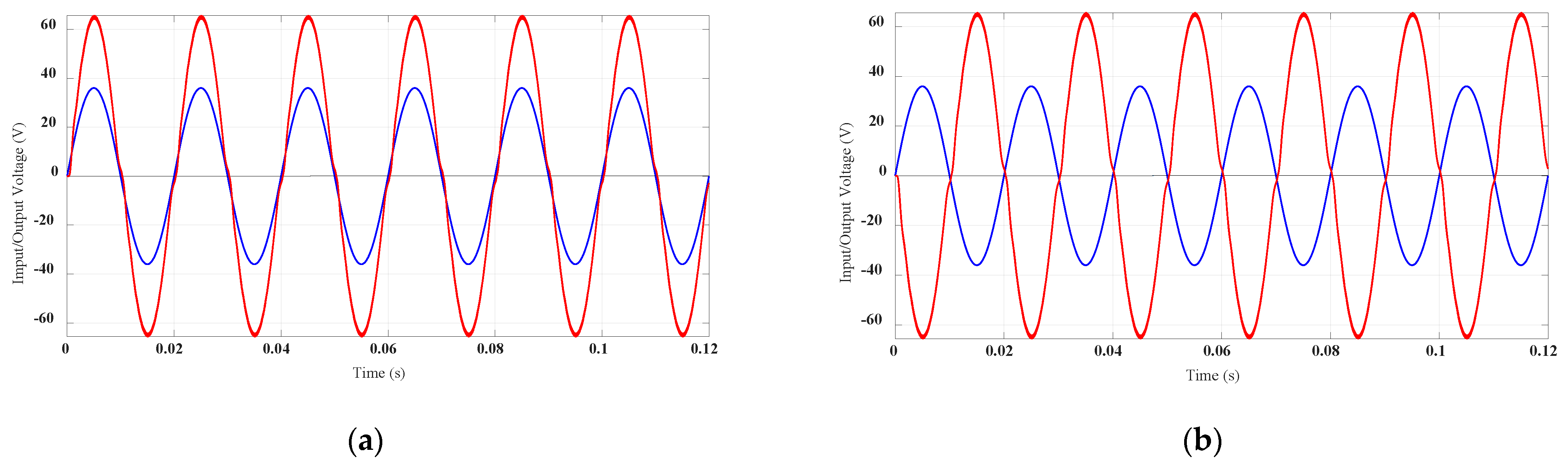
Section 4 compares the performances of the developed converter.
Section 5 explores the design of the filtering components. The result obtained by simulation modeling and practical prototypes are illustrated in
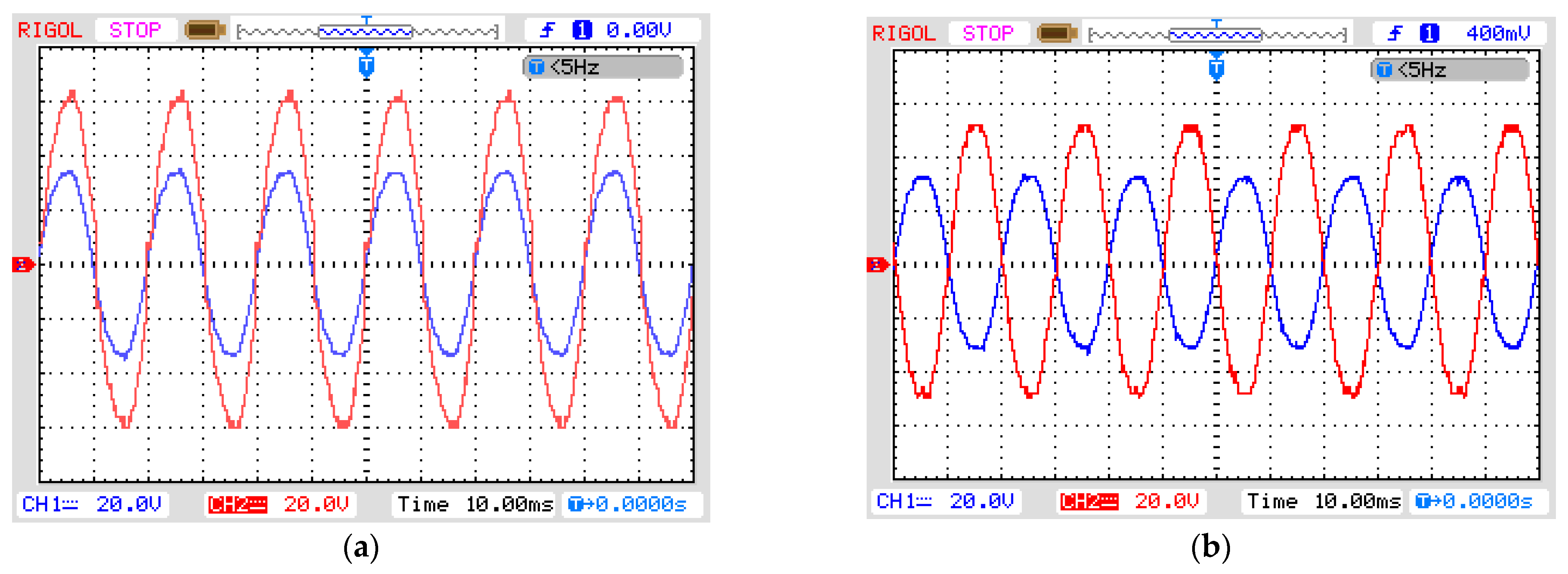
Section 6. The conclusion is stated in
Section 7.
2. Operating Principle and Modes
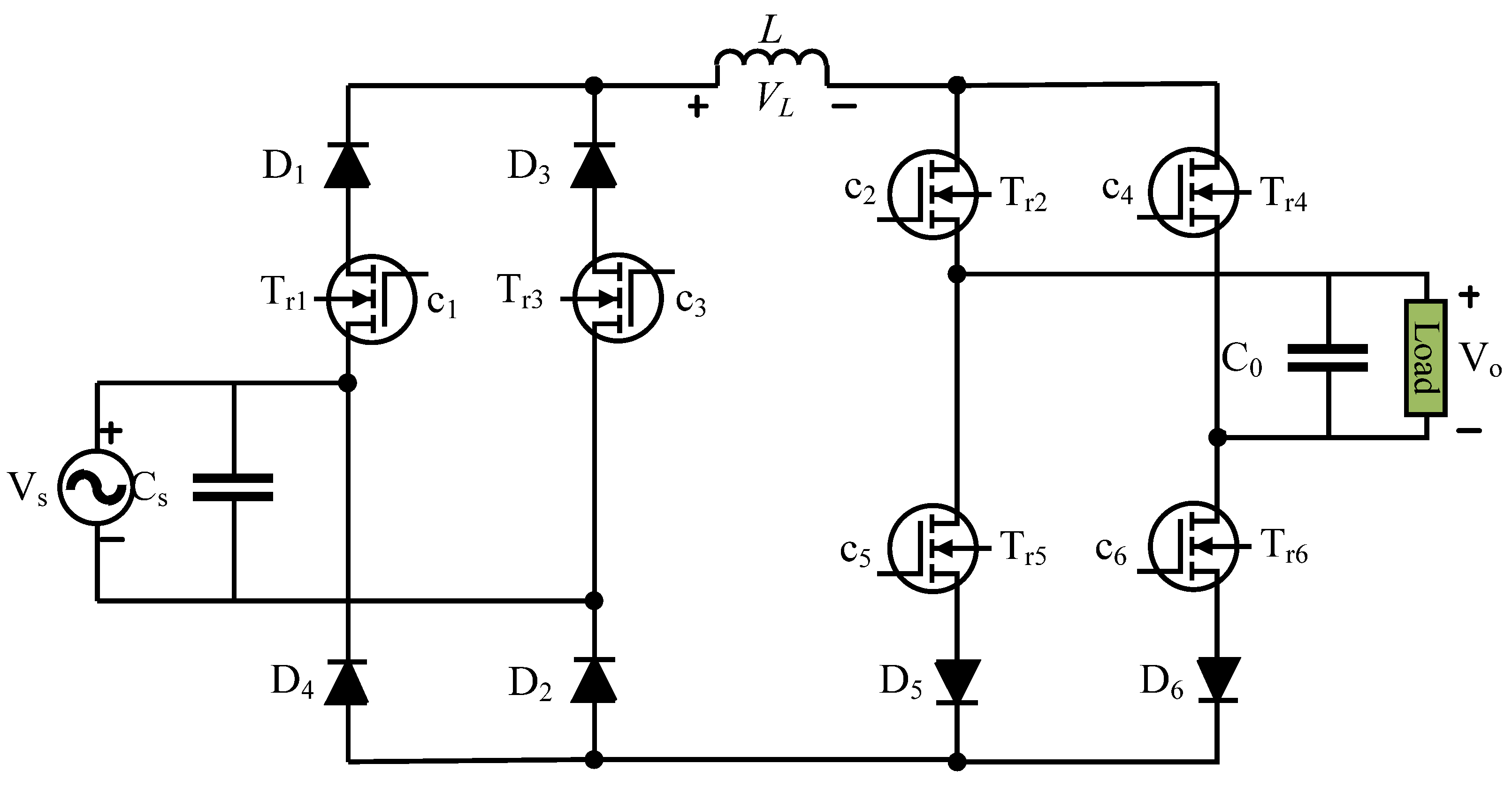
This section describes the working principle and all possible operational modes of the proposed converter in some detail. The developed circuit shown in
Figure 2 is composed of six high-frequency diodes (
D1 to
D6) and six transistors (
Tr1 to
Tr6). This circuit is a modified form of the circuit presented in [
23], where the voltage step-down capabilities are enhanced by adding two more switching transistors (
Tr1 and
Tr3). These transistors are used to convert the constant sinusoidal voltage of the input to its controllable absolute form through PWM control. In any of the operating intervals of the developed circuit, one transistor and one diode operate at high frequency along with the low frequency (input or output frequency) operation of two transistors and diodes. So, there is always the conduction of three diodes and transistors [
11,
20]. There is also the use of one inductor (
L) and two capacitors (one for input (
Cin) and the other for output (
Cout) to tackle the power quality issues. The series connection of diode and transistor forms pairs
D1-
Tr1,
D3-
Tr3,
D5-
Tr5 and
D6-
Tr6. This makes sure the elimination of shoot-through owing to the parallel connection of input and output capacitors, shorting of input or output capacitors. As an example, the connection of diodes
D1 and
D3 avoids the possibility of the direct parallel connection of input and output capacitors. The use of an intermediate inductor avoids the shorting of the input source or capacitor during the situation in which all transistors remain on. This situation may be possible due to the defects in the manufacturing process of the transistors or incorrect control inputs. This problem is normally faced when two transistors must turn on and off in a complementary way. There may be a possibility that turning off transistor may turn off later than turning on transistor. Similarly, the series connection of
D5-
Tr5 and
D6-
Tr6 prevents the shorting of the output capacitor. The details of the operation in dual polarity voltage step-down and step-up modes are explained here with the help of mathematical equations and circuit loops.
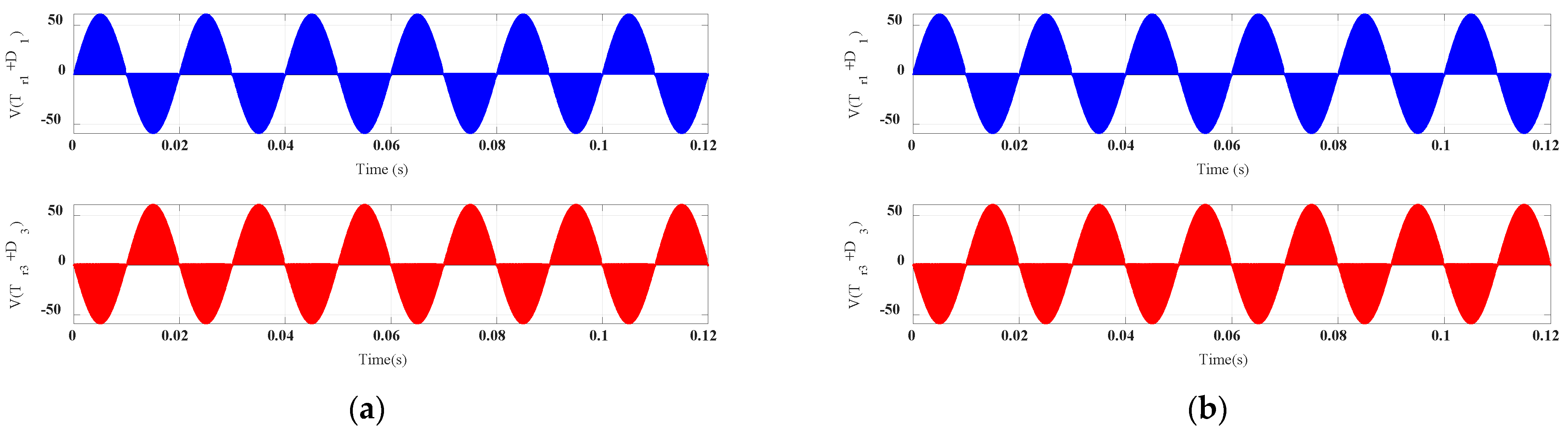
The control strategy shown in
Figure 3a,b to turn on and off the transistors for non-inverting and inverting voltage buck operation, respectively, is almost the same as explained in [
20]. Here all the generated control signals follow the variation in the polarity of the input voltage. For this purpose, the input voltage polarity sensing circuit generates high (5 V) and low (0 V) outputs indicating positive and negative input values, respectively. As an example of voltage step-down operation for both polarities of the output voltage (inverting and non-inverting outputs), the PWM control signals
c1 and
c3 shown in
Figure 3a,b are responsible for power conversion with voltage buck capabilities during the positive and negative input. So, the variation in the instantaneous output voltage is obtained by the high-frequency PWM switching of the transistors
Tr1 and
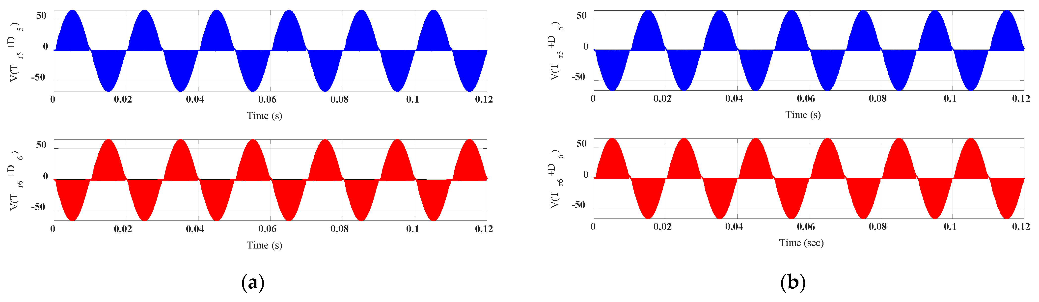
Tr3 during positive and negative input values, respectively. Here the role of the front-end circuit is to convert the constant sinusoidal input voltage into its regulated absolute form. The control of non-inverting and inverting output buck operation is determined from the low-frequency switching operation of the transistors employed in the second stage circuit. For this purpose, the remaining four control signals
c2,
c6 and
c4,
c5 shown in
Figure 3a have logic high and low values throughout the intervals in which input is positive and negative, respectively. It should be noted that control signals
c4 and
c5 are generated in the complementary form of
c2 and
c6. The same control scheme can effectively be employed for an inverting buck operation of the output voltage. It is clear from
Figure 3b that there is no change in the control signal
c1 and
c3 as their role is the same as in non-inverting operation that is to convert the constant sinusoidal input voltage to its controllable absolute value. Here, like a non-inverting operation, the operating states of transistor
Tr2,
Tr6 and
Tr4,
Tr5 realize the inverting output. This task is obtained by reversing the switching states of the control signals
cr2,
cr6 and
cr4,
cr5 with respect to their values of non-inverting operation.
The role of control signals used for voltage buck operation is changed for non-inverting and inverting voltage boost operation. Still, the generated characteristics remain unaltered, as shown in
Figure 4a,b. Here the PWM control of the transistors
Tr1 and
Tr3 is shifted to
Tr5 and
Tr6. Now, transistors
Tr1 and
Tr3 operate at low input frequency and ensure their on-states for positive and negative input voltage, respectively. For non-inverting and inverting voltage boost operation, the role of the front stage circuit is only to transform the constant voltage sinusoidal input to its absolute form. This feature of the operation may be confirmed from the plots of
Figure 4a,b There is no change in states of the control signals
c1 and
c3 for the operation in which the output voltage is a non-inverted or inverted form of the input voltage. The inverted and noninverted form of the output depends on switching states of
c2,
c4 and
c5,
c6. The switching state of the control signals
c6 is swapped with
c5 and
c4 is swapped with
c2 once the output is changed from non-inverting to inverting boost form and vice versa.
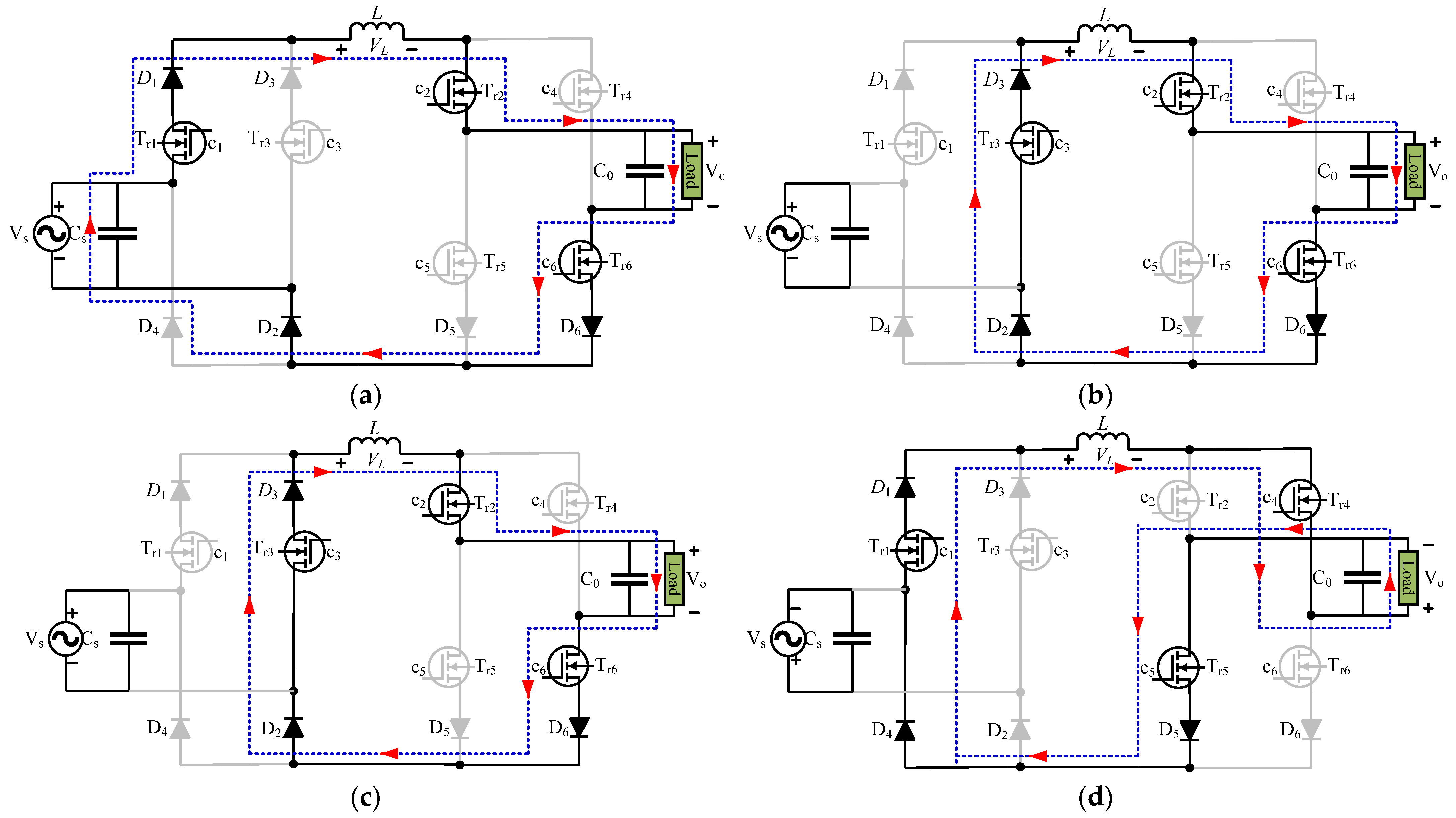
2.1. Non-Inverting and Inverting Buck Operation
This section provides detail on how the rms value of the input voltage at the output is regulated in voltage step-down capabilities with PWM control. Here the output rms voltage is adjusted from the maximum value of the input rms to some lower value. This task is achieved with PWM control of the switching transistors
Tr1 and
Tr3 for positive and negative input, respectively. The low frequency (input or output) operation of transistors
Tr2,
Tr4,
Tr5 and
Tr6 is responsible for in-phase or out-phase outputs. The circuits of
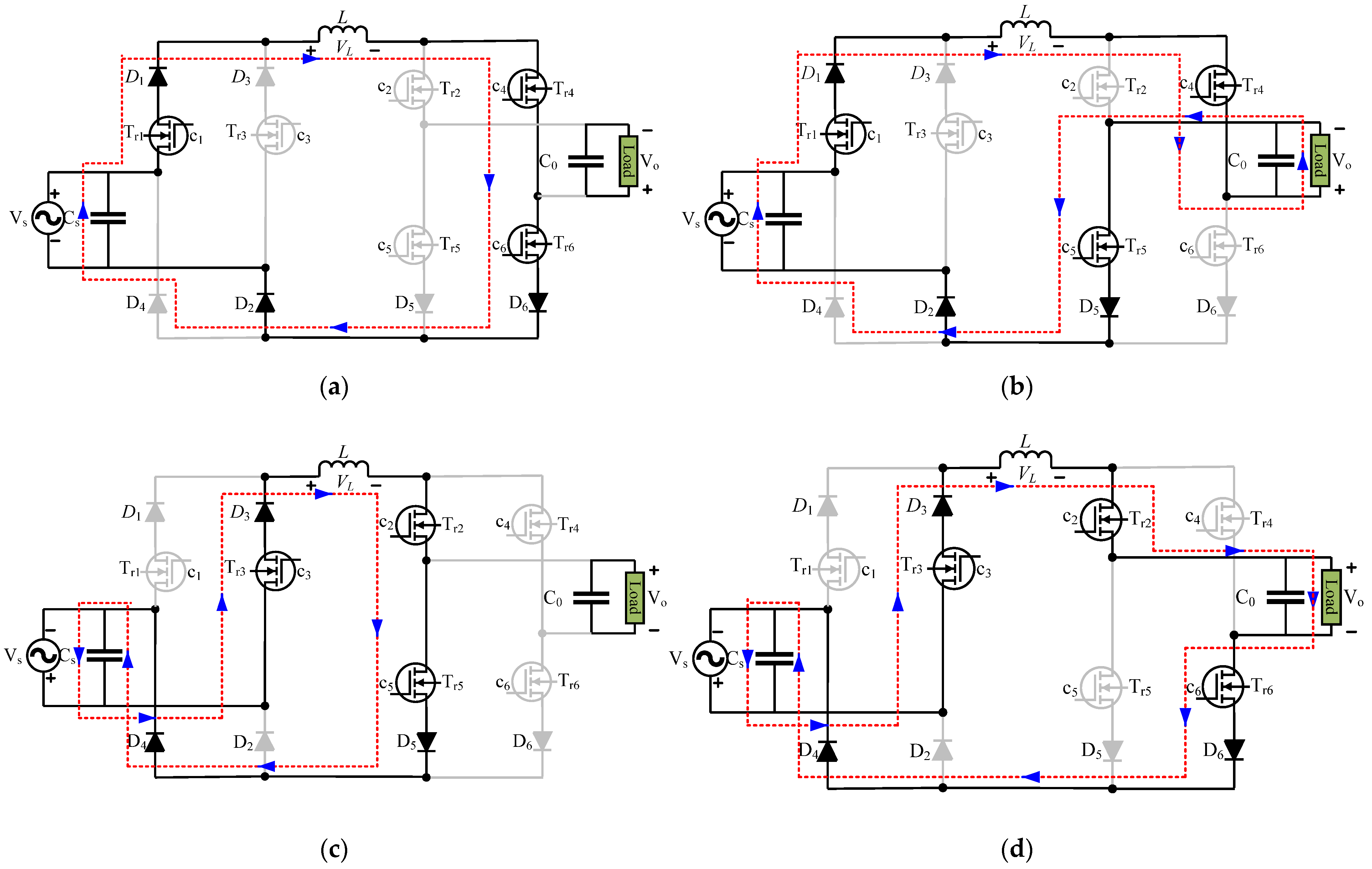
Figure 5 comprehensively illustrate the voltage step-down operation indicating how the input power is supplied to load.
Figure 5a–d show the power transferring loops for non-inverted output for positive and negative half-cycles input voltage, respectively.
For positive input, the on-state role of the semiconductor devices
Tr1,
D1,
Tr2,
Tr6,
D6, and
D2 facilitate the power flow from source to load. The voltage drop across the inductor during the conducting interval (
tc) of the PWM signal is the difference of the input and output voltage as observed in Equation (1).
The turning on of the transistor
Tr3 facilitates the continuous conduction of inductor current as the reverse bias diode
D3 turns on in the non-conducting interval (
tnc) of the PWM signal. During this interval, the absorbed power of the inductor is supplied to load, as may be found from the power supply loop of
Figure 5b. Now the value of the inductor voltage is changed to output voltage level
Vo.
A similar analysis may be used to express the voltage buck operation for negative input and determine the value of inductor voltage during conducting and non-conducting PWM intervals.
Figure 5c expresses the power supply path from source to load via the conduction of
Tr3,
D3,
Tr4,
D4,
Tr5, and
D5. The continuous conduction of inductor current is confirmed by maintaining the transistor
Tr1 in conducting state because the diode
D1 is only reverse biased as long as
Tr3 is on. The transfer of the inductor’s stored power is recovered by the conduction of
Tr1,
D1,
Tr4,
D4,
Tr5, and
D5, as expressed in
Figure 5d. The realization of the inductor voltage during the conducting and non-conducting interval is accomplished as
The values of these voltages may be regarded as constant as the selected switching frequency is much higher (for example, 25 kHz) than the input or output frequency (50 Hz). The average value of the inductor voltage in the steady-state condition in one switching interval is always zero, and this result may be utilized to find the relation of output voltage with respect to the input voltage. Here
D and
T are the duty ratio and the period of the PWM signal, respectively.
This implies that in a switching interval (
T), the inductor volt-second product is zero. For non-inverting voltage buck operation with any polarity of the input voltage, we get
so
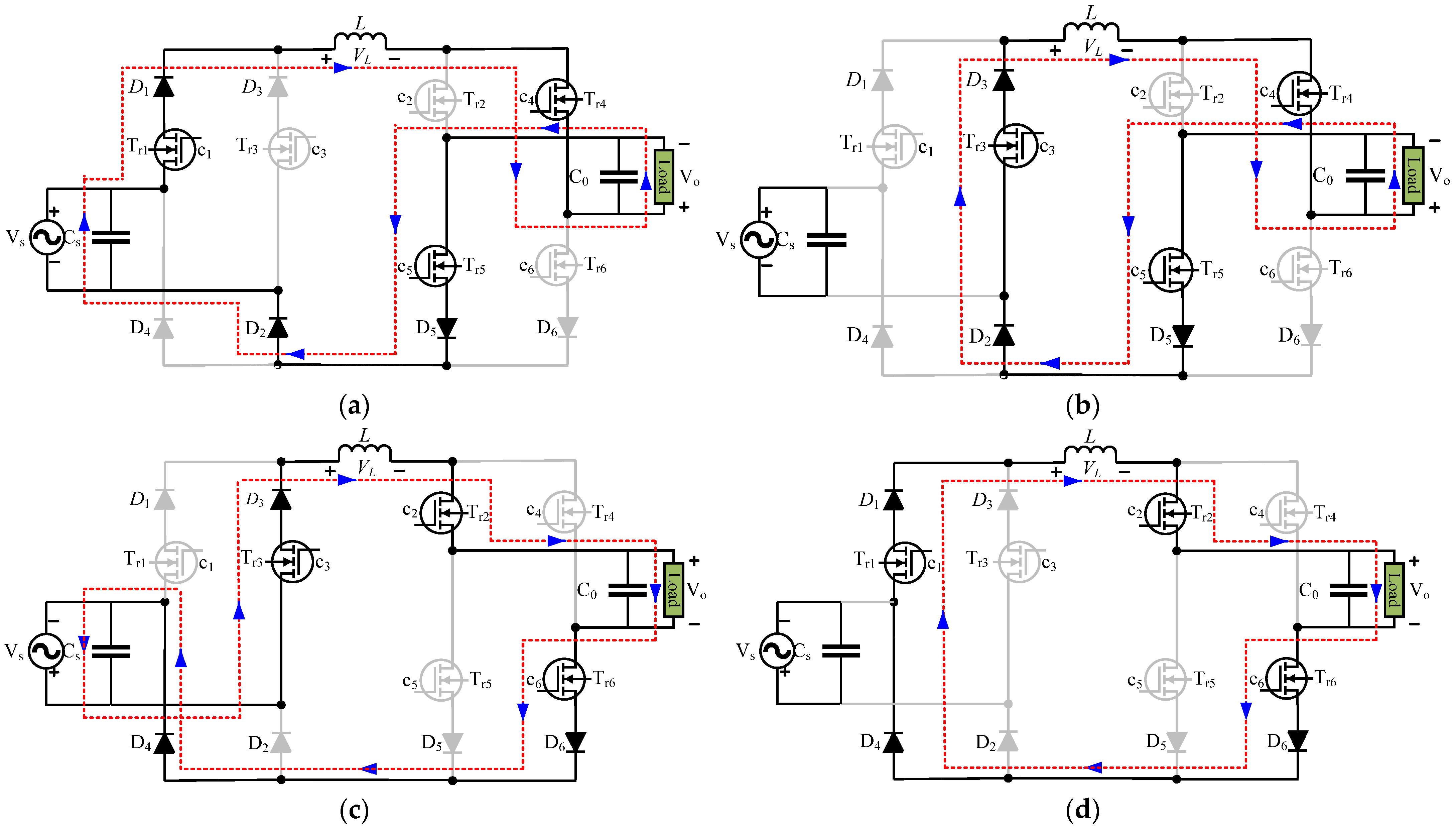
By employing a similar methodology, the voltage step-down inverting behavior of the proposed circuit can also be validated with equivalent circuits and mathematical equations. This mode produced an inverted form of the input voltage at the output, and this is simply turning on the low-frequency transistors
Tr4,
Tr5 and
Tr2,
Tr6 for positive and negative input voltage by maintaining the switching role of
Tr1 and
Tr3 unchanged. The power transfer loops of
Figure 6a–d explain how the variable inverting outputs with voltage buck capabilities are obtained from a constant input voltage.
The mathematical validation of this behavior can be proved by employing a similar approach as used for a non-inverting buck operation. The value of the inductor voltage during the conducting and non-conducting interval for any value of the input voltage may be depicted as
Average inductor voltage gives
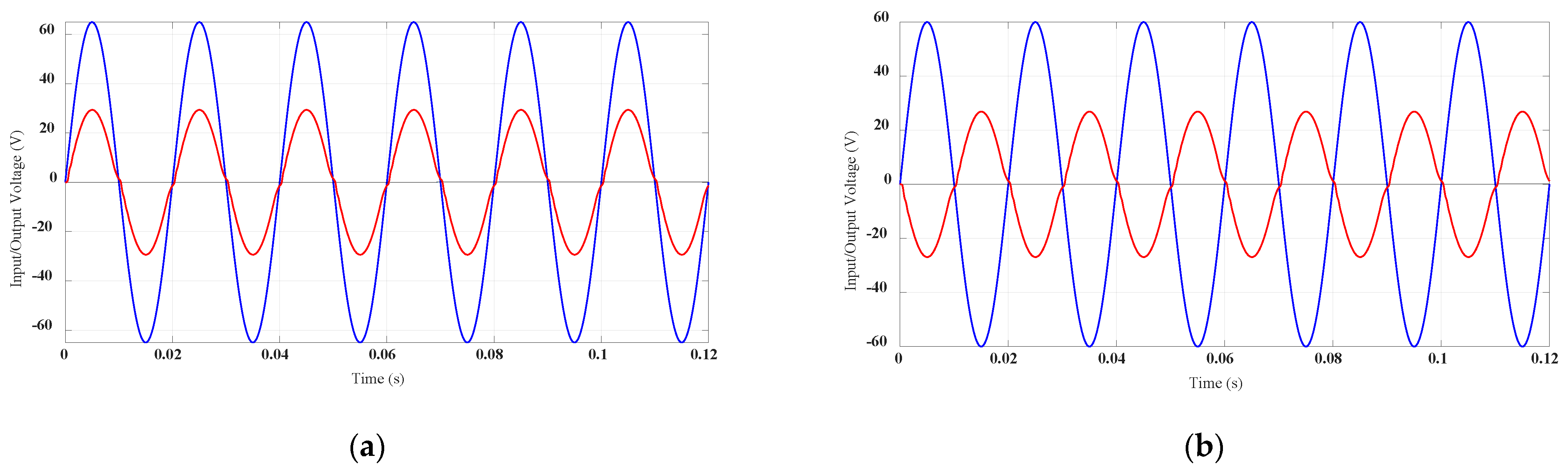
The results of Equations (10) and (16) validate the voltage non-inverting and inverting buck operation, indicating that output is always controllable with the PWM control.
2.2. Non-Inverting and Inverting Boost Operation
The operation in this mode helps to increase the voltage of any polarity at the output with respect to the input voltage, and this voltage stabilization depends on the PWM control. The switching arrangement to govern the on and off behavior of the transistors is shown in the control schemes of
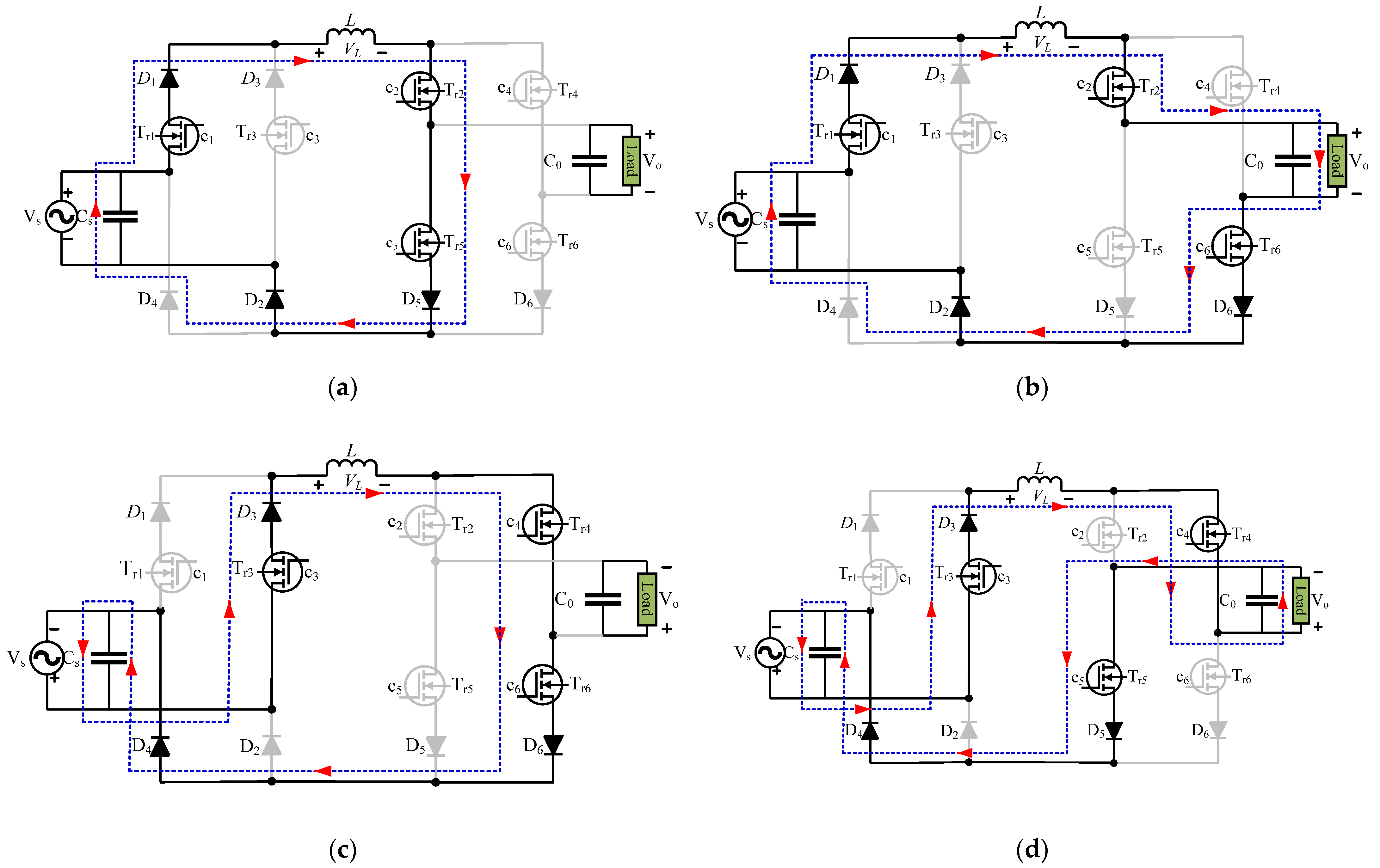
Figure 4. It has already been stated that the control schemes used in the realization of voltage buck operation can be effectively employed for voltage boost operation. The power flow loops of
Figure 7a–d can be used to demonstrate the non-inverted voltage boost behavior for any value of input voltage.
For positive input voltage, the PWM control of transistor
Tr5 stores power in the inductor via the power flowing loop formed by the conduction of
Tr1,
D1,
Tr2,
D2,
Tr5, and
D5 that may be seen from
Figure 7a. In the non-conducting interval of the PWM control, the inductor and source get connected in series with the load through the operating devices
Tr1,
D1,
Tr2,
D2,
Tr6, and
D6 that may find in the loop of
Figure 7b. Here switching of transistor
Tr6 during conducting and non-conducting intervals of PWM control ensures the continuous inductor current as series diode
D6 operates in a complementary way of transistor
Tr5. A similar operation can be explored for negative input as depicted in the power flow loops of
Figure 7c,d. The value of the inductor voltage during the conducting and non-conducting intervals of the PWM control is used to find out the variation in the output voltage with respect to the constant input voltage. That is to say
By finding the average of inductor voltage
The voltage inverting operation can also be supported with the same control signals to generate non-inverting outputs. The conduction of
Tr1,
D1,
Tr4,
D2,
Tr5,
D6 and PWM control of
Tr6 during positive input helps to store power in the inductor, as may be viewed from
Figure 8a. Then turning off of
Tr6 and forward biasing of
D5 along with previously conducting devices
Tr1,
D1,
D2,
Tr4,
Tr5 connect the source, inductor, and load in series as may be viewed from
Figure 8b. The detail of inverting behavior for negative input may view from the power flow loops of
Figure 8c,d plotted during the conducting and non-conducting intervals of the PWM control, respectively.
The validation of inverting voltage gains for both input polarities may also be formulated with the help of inductor voltage during the conducting and non-conducting intervals of the PWM control.
Averaging of inductor voltage is
The comparison of Equations (22) and (28) proves stabilization of the bipolar voltage capabilities of the output voltage with PWM or duty cycle control.
3. Consideration of the Conversion Losses
The losses in any power converting system depend on the losses caused by the filtering components, solid-state devices, and gate control circuits. Power losses produced by the filtering component can be ignorable as they have a low value of their internal resistances. The losses produced by the solid-state transistors and diodes are the sum of their switching (Psw) and conduction losses (Pcon).
The switching losses depend on the switching frequency and the value of the voltages and currents at which they change their states from off to on and vice versa. These losses in transistors are a function of their current and voltage rise and fall characteristics and but in diode, they are related to their reverse recovery characteristics. The instantaneous voltage and currents in any switching period can be considered constant as switching periods are much less than that of the periods of the output or input voltages. The switching losses of a MOSFET and diode may be calculated by considering the procedure developed in [
24].
Here
VDS and
IDS are the drain to source voltage and current, respectively. The
trise and
tfall are the intervals in which the drain current increases to the final steady-state value and decreases to the minimum value, respectively.
QRR is the amount of reverse recovery charge that flows across the junction and
VRR is the reverse voltage across the junction during the reverse recovery intervals. The value of the conduction losses for a MOSFET and diode is calculated as
The conduction losses of a transistor and diode depend on the value of their internal resistances and rms and average currents.
The losses produced by the gate control circuits (
PGC) are the sum of isolated DC supplies and gate drivers. That may be considered constant as they depend on their number. There is a need for only six gate control circuits in the developed topology but the execution of the circuit in [
20] requires the use of eight such circuits. There is the conduction of four low-frequency transistors and diodes along with the high-frequency switching operation of two transistors and diodes during one output interval. The total conversion losses of the developed circuit and circuit reported in [
11,
20] may be approximated as
The elimination of two gate control circuits in the developed circuit not only reduces the conversion losses but also drastically lowers the circuit’s overall volume and cost.
5. Design Description
The basic purpose of using the input and output capacitance is to eliminate the unwanted voltage components. On the other hand, the role of the inductor is to minimize the ripple contents in the current. The inductor is also used as an energy-storing element and helps to tackle the shoot-through issue as well. The design of these elements depends on the input voltage (
Vs ), average value of the inductor current (
IL), output current (
Io) or impedance (
ZL), switching frequency (
fs), inductor ripple current factor (
ki) that is normally 20% of inductor current and output voltage ripple factor (
kv) that may take 10% of the output or input voltage. The role of the developed circuit is to step down and step up the input voltage at the output. The design of the filtering components is obtained with respect to the high value of the voltage and currents of the developed circuit. In voltage buck operation, the average value of the inductor and output currents are the same but in boost mode, the average value of the inductor is greater than the average output current with the relation given in Equation (35). The value of the duty cycle and switching frequency is taken 0.5 and 25 kHz, respectively. The values of the filtering components are computed with a similar approach stated in [
19,
25].
The value of the inductor is calculated for an input voltage of 65 V, a duty cycle of
D = 0.5, a switching frequency of 25 kHz, and a maximum value of the inductor current of 2 A.
The ripples in the output voltage are directly related to the value of the output capacitance whose value is computed for an output voltage of 65 V and output current of 1 A as
The value of the input capacitance depends on the duration in which it is discontinuous. The input current is continuous in voltage boost mode and is only discontinuous in voltage buck mode. Its value is calculated with an input current of 0.5 A as
So, the values of the inductor and output and input capacitance are approximated for computer and practical results as 1 mH, 4.7 µF and 1 µF, respectively.


 ,
, 


