Article

CdS/PbSe Heterojunction Made via Chemical Bath Deposition and Ionic Exchange Processes to Develop Low-Cost and Scalable Devices

by
José Antonio Heredia-Cancino
1,*,
Oscar Salcido
2,
Ricardo Britto-Hurtado
1,3,
Sayra Guadalupe Ruvalcaba-Manzo
3,
Ramón Ochoa-Landín
4 and
Santos Jesús Castillo
3
1
P.E. Ingeniería Mecatrónica, Universidad Estatal de Sonora, Av. Ley Federal del Trabajo s/n, Col. Apolo, Hermosillo C.P. 83100, Sonora, Mexico
2
P.E. Ingeniería Industrial en Manufactura, Universidad Estatal de Sonora, Av. Ley Federal del Trabajo s/n, Col. Apolo, Hermosillo C.P. 83100, Sonora, Mexico
3
Departamento de Investigación en Física, Universidad de Sonora, Blvr Luis Encinas s/n, Col. Centro, Hermosillo C.P. 83000, Sonora, Mexico
4
Departamento de Física, Universidad de Sonora, Blvr Luis Encinas s/n, Col. Centro, Hermosillo C.P. 83000, Sonora, Mexico
*
Author to whom correspondence should be addressed.
Appl. Sci. 2021, 11(22), 10914; https://doi.org/10.3390/app112210914
Submission received: 23 September 2021 / Revised: 17 November 2021 / Accepted: 17 November 2021 / Published: 18 November 2021
(This article belongs to the Special Issue Recent Advances in Application of Coatings and Films)

Abstract

:
Complete optoelectronic devices present major difficulties to be built by aqueous chemical deposition. In this work, a ITO/CdS/PbSe heterostructure was developed, depositing CdS over an ITO-coated substrate via a chemical bath deposition (CBD) technique. The next step involved the growth of a plumbonacrite film over CdS via CBD, where the film acted as a precursor film to be converted to PbSe via ion exchange. The characterization of each material involved in the heterostructure were as follows: the CdS thin films presented a hexagonal crystalline structure and bandgap of 2.42 eV; PbSe had a cubic structure and a bandgap of 0.34 eV. I vs. V measurements allowed the observation of the electrical behavior, which showed a change from an ohmic to diode response by applying a thermal annealing at 150 °C for 5 min. The forward bias of the diode response was in the order of 0.8 V, and the current-voltage characteristics were analyzed by using the modified Shockley model, obtaining an ideality factor of 2.47, being similar to a Schottky diode. Therefore, the reported process to synthesize an ITO/CdS/PbSe heterostructure by aqueous chemical methods was successful and could be used to develop optoelectronic devices.

1. Introduction

Optoelectronic devices based on the semiconductors CdS and PbSe have been widely used throughout the technological revolution. The main devices, in the case of PbSe, are infrared detectors used for different applications [1,2,3,4,5,6]. CdS, meanwhile, is used in transistors, visible light detectors and, particularly, as a window material for solar cells [7,8,9,10,11,12,13,14]. These materials are produced by several methods with a wide range of costs; of these, being used mainly, CBD is the lowest cost method for CdS. However, the methods used to deposit PbSe are expensive, since they mainly use physical techniques [15,16,17]. These materials are also compatible to produce heterojunctions and could open a new path in the manufacture of optoelectronic devices for different applications [18,19,20]. Usually, heterojunctions are not synthesized using methods in aqueous solutions; such methods involve a great difficulty in optimization, which has led to little use despite their low cost and the good quality of the films that they generate [21,22,23,24]. Weng et al. [18] developed a CdS/PbSe heterojunction for high-temperature mid-infrared photovoltaic detector applications. They deposited CdS via CBD and PbSe via Molecular Beam Epitaxy (MBE) techniques. Ling et al. [19] reported a PbSe/CdS/nitrogen-doped TiO2 nanorod array photoelectrode, in which CdS and PbSe were deposited by the Chemical Vapor Deposition (CVD) technique, using N2 and H2 atmospheres, respectively. Qiu et al. [20] reported a PbSe-QDs/CdS/CdSe:In/Si heterojunction photodiode. They used quantum dots of PbSe instead of a film; however, the response of their photodiode had promise for the production of infrared devices. Most of the articles used the CVD technique to create the heterojunction, due to the difficulty of depositing a bilayer by chemical methods. In this sense, the goal of this work is to synthesize a CdS/PbSe heterojunction through chemical methods to develop low-cost and scalable devices. The characterizations carried out for each material were by X-ray Diffraction (XRD), Scanning Electron Microscopy (SEM), Energy Dispersive Spectroscopy (EDS), and UV-Vis techniques, for structural, morphological and chemical composition, and optical properties, respectively. Finally, the response of the CdS/PbSe heterojunction was analyzed by current–voltage characterization using the modified Shockley model.

2. Experimental

2.1. Reagents

All reagents were supplied by Sigma-Aldrich. The preparation of the CdS thin films was carried out using the following reagents: cadmium chloride (CdCl2, purity 98%); sodium citrate (Na3C6H5O7, purity 99%); potassium hydroxide (KOH, purity 85%); and thiourea (CH4N2S, purity 99%). For PbSe films the reagents used were: lead acetate (Pb(CH3COO)2, purity 99%); sodium hydroxide (NaOH, purity 98%); triethanolamine (C6H15NO3, purity 98%); rongalite (CH3NaO3S, purity 98%); and selenium powder (Se, purity 99%).

2.2. Synthesis Procedure

The semiconductor layers used to form the CdS/PbSe heterojunction were the product of previous work by our research group, which were published separately and have been presented here as a heterojunction. For more details see the following references [25,26].
The ITO/CdS/PbSe heterojunction was prepared in three stages: the first consisted of depositing a CdS thin film on ITO, which is an intrinsic n-type semiconductor; then the next two stages were used to deposit the PbSe film on ITO/CdS, where PbSe was predicted to be a p-type semiconductor, therefore CdS and PbSe stacked could form a p-n junction [27,28]. In detail, for the first stage the CBD technique was used to grow a CdS thin film (100 nm) on a commercial glass substrate coated with ITO (500 nm). The substrates were cleaned using industrial soap and rinsed with deionized water. The recipe used to grow the CdS thin films in a 100 mL beaker consisted of the following: 10 mL CdCl2 (0.05 M); 20 mL Na3C6H5O7 (0.05 M); 5 mL KOH (0.3 M); 10 mL CS(NH2)2 (1 M); and 55 mL deionized water. The reaction temperature was 70 °C and the deposition time was 90 min.
The next stage concerned the deposition of a plumbonacrite film, Pb5(CO3)3O(OH)2, on the CdS layer. The recipe used to make the plumbonacrite film in a 100 mL beaker was as follows: 5 mL Pb (CH3COO)2 (0.5 M); 5 mL NaOH (2 M); 2 mL C6H15NO3 (1 M); and 82 mL deionized water. The reaction temperature and time were 54 °C and 24 h, respectively, to achieve the CdS/Pb5(CO3)3O(OH)2 heterojunction.
The third and last stage consisted of the immersion of the bilayer CdS/Pb5(CO3)3O(OH)2 in a rich selenium ion solution to promote an ionic exchange to achieve the CdS/PbSe heterojunction. The preparation of the selenium ion solution was carried out at room temperature by mixing 10 mg of selenium powder in a solution with 10 mL CH3NaO3S (1 M), 10 mL Na3C6H5O7 (1 M), and 10 mL of deionized water in a sealed tube and shaking vigorously until a clear solution is obtained. This process took about 5 min. Figure 1 depicts the heterostructure design that was built as a final product.

2.3. Characterization

A Rigaku D/max-2100 and Rigaku/Ultima IV X-ray diffractometers, to obtain the X-ray Diffraction (XRD) patterns of the films. The surface morphology and chemical composition of the samples were analyzed by Scanning Electron Microscopy (SEM) and X-ray Energy Dispersive Spectroscopy (EDS), using a field-emission scanning electron microscope JEOL JSM-7800F equipped with a Bruker XFlash 6|60 EDS spectrometer. Optical characterization was carried out by UV-vis, Cary WIN 60 and JASCO, FT/IR-5300. I vs. V measurements for the ITO/CdS/PbSe heterostructure were performed by Probing Solutions PSI200 Test Station.

3. Results and Discussion

3.1. XRD Analysis

Most of the CdS or CdS/PbSe-performed characterizations were carried out on corning glass substrates to avoid wasting glass substrate coated with ITO. Only I vs. V characterization was performed using ITO as a front contact to close the circuit of the CdS/PbSe device.
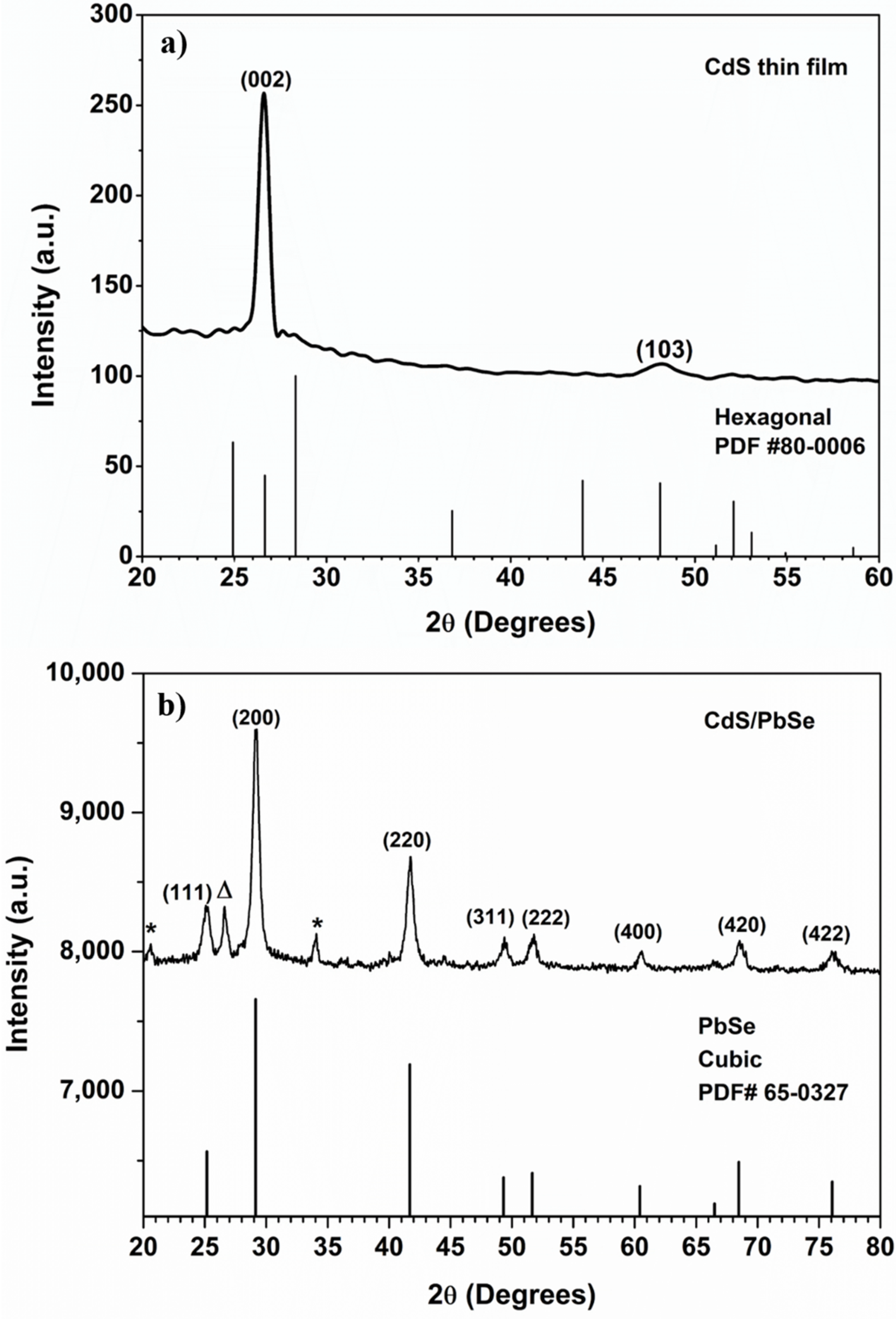
The XRD diffractograms of synthetized CdS and CdS/PbSe are presented in Figure 2. A hexagonal crystalline structure was observed in the CdS thin film (PDF# 80-0006, Cu X-ray source), with a preferential orientation crystalline plane (002) at 26.87° (Figure 2a). We also observed another diffraction peak at 48.24° corresponding to the same crystalline structure and the crystalline plane (103). No other diffraction peaks appear, indicating the absence of impurities during the deposition of CdS. Figure 2b shows the XRD of the heterojunction CdS/PbSe, obtained by converting plumbonacrite to PbSe by ionic exchange The XRD pattern match with the mineral phase of PbSe was called clausthalite (PDF# 65-0327, Cu X-ray source), which corresponded to a cubic crystalline structure with a preferential orientation crystalline plane (200) at 29°. As can be shown, only one diffraction peak of CdS was detected and denoted by Δ , which corresponds to the crystalline plane (002) as aforementioned. Additionally, two extra diffraction peaks at 20.5 and 34°, labeled with *, appeared, which correspond to crystalline planes (−101) and (111) of the PbSe molybdenite monoclinic crystalline phase (PbSe + 4O3), according to the PDF# 15-0462 (Cu X-ray source). Therefore, the conversion from plumbonacrite to PbSe can be stated as successful, since no other diffraction peaks related to plumbonacrite appeared [26].

3.2. SEM and EDS

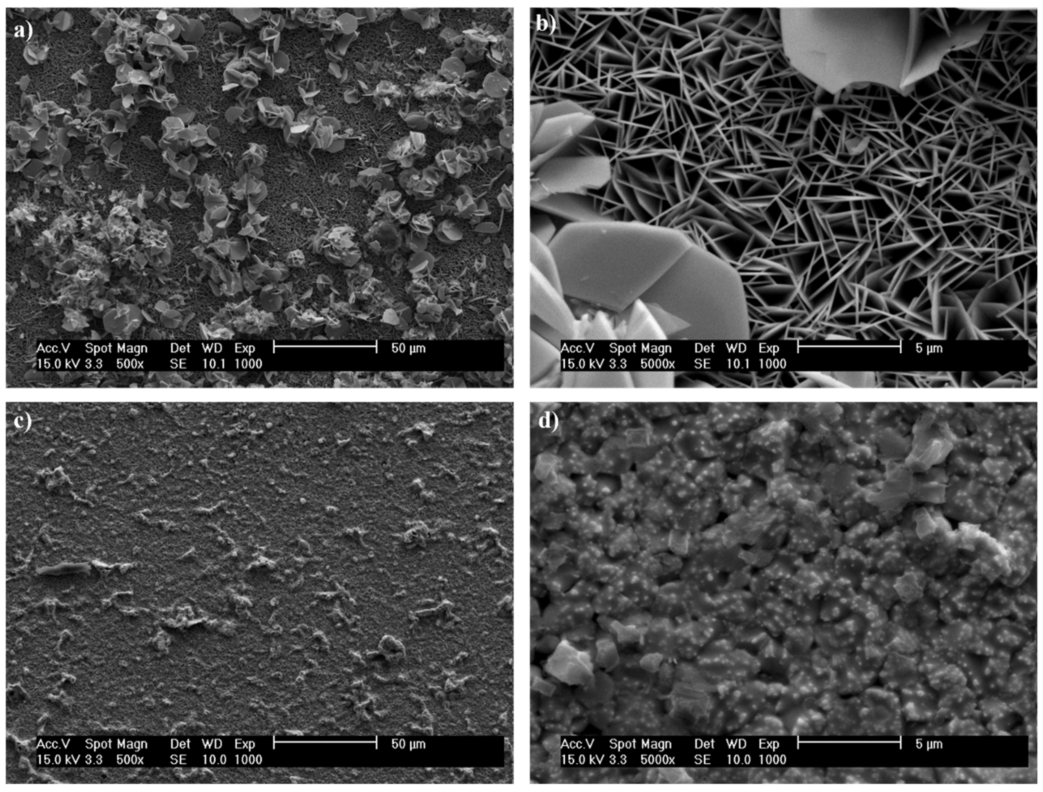
Figure 3 presents SEM micrographs of the surface morphology of the upper layer of the heterojunction before and after the ionic exchange with selenium. Figure 3a,b shows a flake-like morphology, corresponding to plumbonacrite film at 50 and 5 μm scale, respectively. Meanwhile, Figure 3c,d exhibits the change in morphology after transformation to PbSe, where the “flakes” of the precursor film disappear, showing a composite surface consisting of a flat background plus a roughness with different shapes. As can be observed in Figure 3d, there are cubic crystalline shapes with sizes around 1–2 μm, agreeing with the XRD results for PbSe.
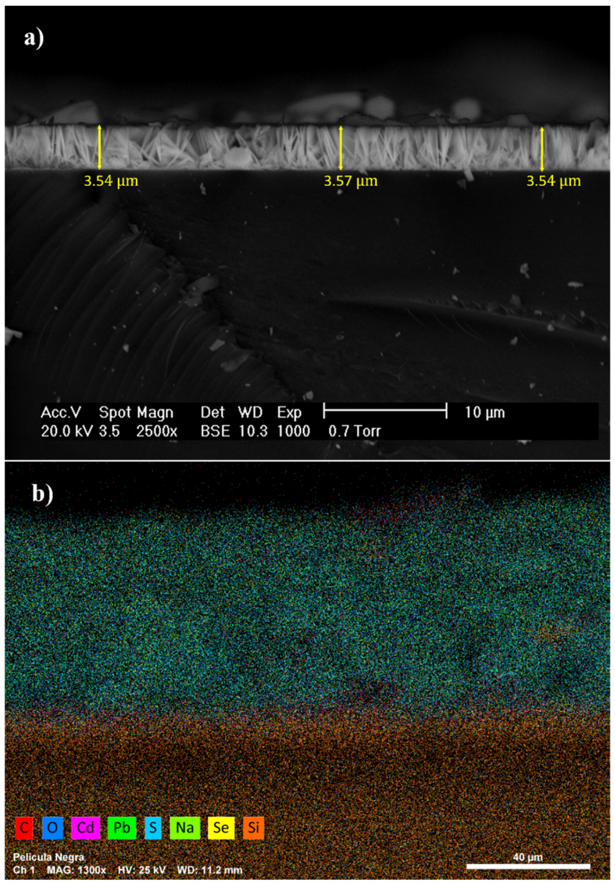
A cross-sectional view of CdS/Pb5(CO3)3O(OH)2 was used to estimate its thickness, which was found to be about 3.5 μm (Figure 4a). This value is similar to that obtained when plumbonacrite is deposited on corning glass substrates, as we have previously reported [26]. Figure 4b shows a perspective view of EDS elementary mapping of the CdS/PbSe heterojunction, with only a qualitative assessment of the present elements and their distributions. It evidences the presence of CdS thin film as the first layer of the heterojunction, followed by a second layer formed from PbSe in agreement with XRD results. On the other hand, the elemental mapping analysis of EDS exhibits a high concentration of sulfur in the upper layer, which does not correspond to the chemical composition of the PbSe film. Nonetheless, this result is due to the superposition of the Kα band of sulfur with the Mα band of lead, whose values are 2.309 and 2.342 keV, respectively.

3.3. Optical Absorption

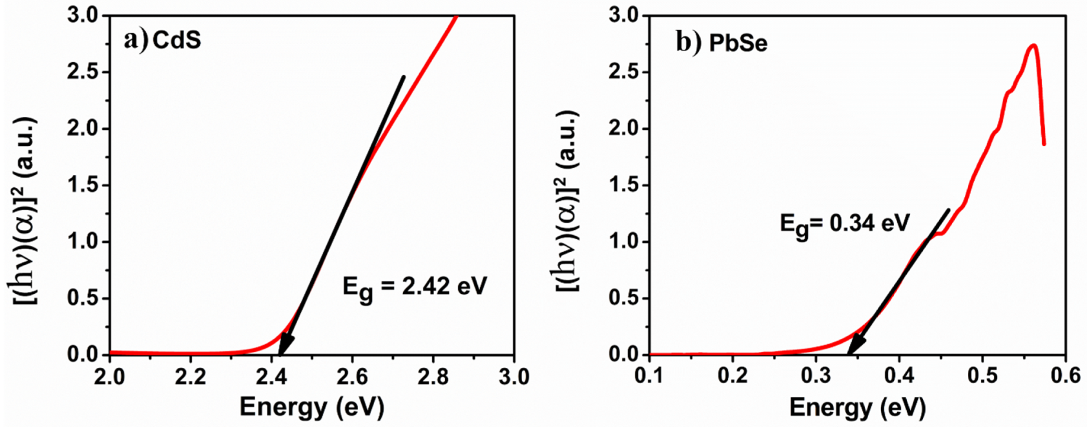
One of the main characterizations for semiconductors is the energy bandgap. Figure 5 exhibits the result of Tauc procedure to calculate the direct energy bandgap for each involved material deposited on glass: (a) CdS and (b) PbSe. To measure the energy bandgap for CdS and PbSe, it was necessary to use two different spectrophotometers, one for UV-Vis and one for medium-far infrared regions, respectively. For CdS thin film, the value obtained was 2.42 eV, which agrees with values reported in the literature; for the PbSe film, the bandgap was 0.34 eV, which is slightly higher than the 0.27 eV reported value for PbSe bulk bandgap.

3.4. Electrical Response

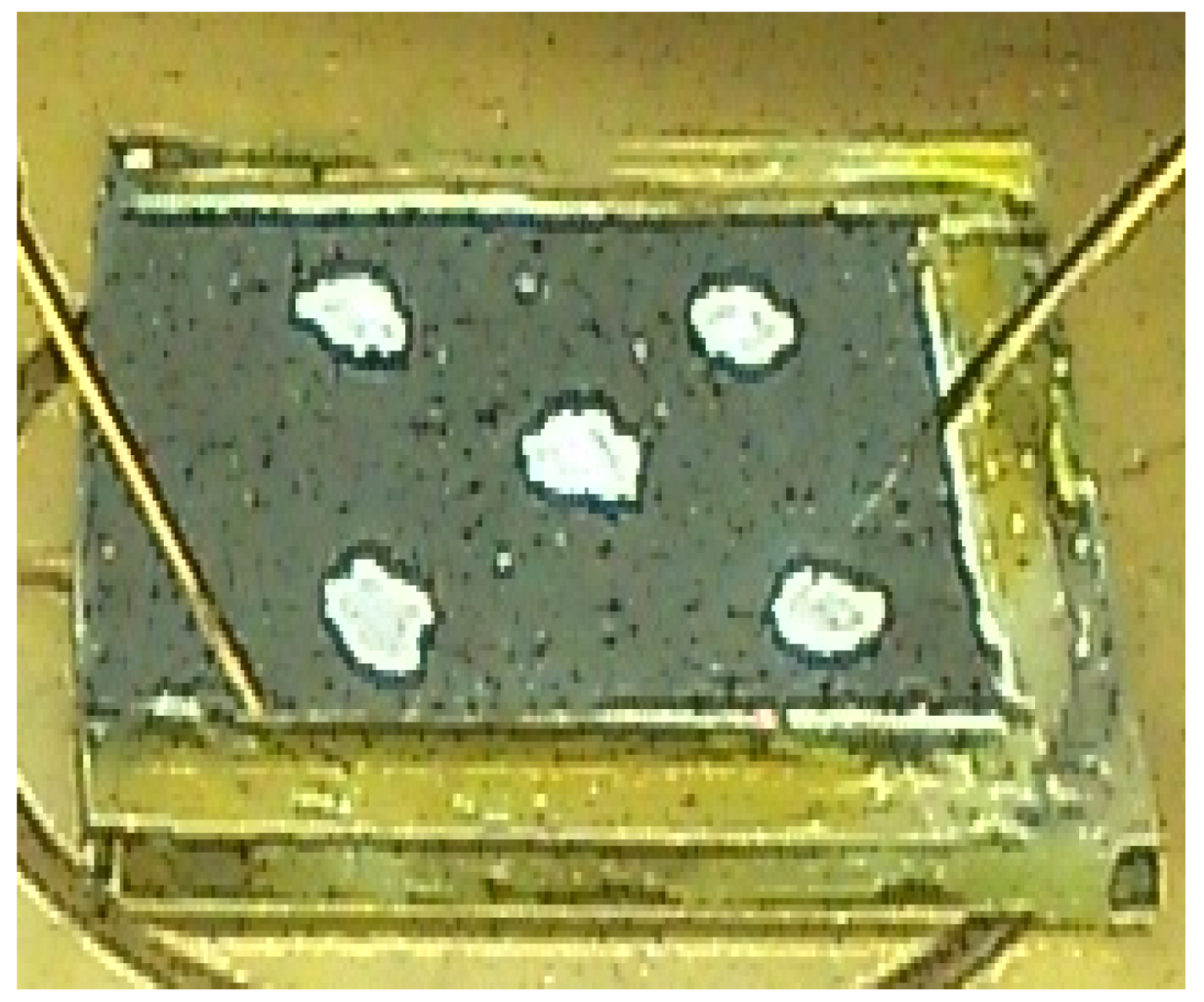
The final structure to produce the diode was carried out using a substrate coated with ITO as a transparent conductor for frontal contact to produce the ITO/CdS/PbSe heterostructure. Subsequently, silver electrodes were deposited on the PbSe as rear contacts to perform the I vs. V characterization under darkness conditions (Figure 6).
The first measurement presented an ohmic behavior, meaning that the p–n junction CdS/PbSe did not form a depletion zone, possibly because there was no full coupling among them (Figure 7a). Thus, an annealing treatment was performed to promote the layers’ diffusion, with atmospheric conditions of 150 °C for 5 min. The result of the thermally annealed heterostructure was the forward bias response of a typical diode behavior (Figure 7b). It is important to mention that the effect of mild thermal annealing was to change the response from ohmic to diode behavior, since only 5 min at a relatively low temperature was needed to produce a better diffusion between the semiconductors to improve the p-n junction.
According to Figure 7b, the forward bias of the diode response was in the order of 0.8 V, and the current–voltage characteristics were analyzed by using the modified Shockley model [29,30,31]:
I = I s [ exp ( V R s I η V T ) 1 ]
I s = A e A T 2 exp ( ϕ B V T )
where Is is the saturation current, VT = kT/q is the thermal voltage, k is the Boltzmann’s constant, q = e is the elementary charge, T is the absolute temperature (300 K), η is the ideality factor, Rs is the series resistance, Ae is the effective area of the diode (625 mm2), A∗ is the effective Richardson’s constant and Φ B is the barrier height. The diode parameters were extracted by fitting this model to the experimental curve, as shown in Table 1.
The ideality factor obtained was 2.47 for the synthetized device, while Weng et al. [18] reported an ideality factor of 1.79 for the same CdS/PbSe p–n heterojunction but placed on a Si wafer with ultrathin CaF2 (2 nm). They grew CdS thin film via CBD in the method as used in this study, while their PbSe film was set down via the MBE technique, which is a more expensive, complex, and non-scalable technique compared to our deposition method. The difference in the ideality factor may be attributed to the diffusion between ITO (500 nm) and CdS (100 nm) layers, which could form a deep combination among the metallic oxide and semiconductor behaving as a metal oxide semiconductor (MOS) hybrid layer, that together with PbSe produce a heterostructure with an ideality factor η > 2, that is categorized as a Schottky diode according to the literature. Also, ideality η > 2 can be attributed to defects and imperfections that affect the recombination current, which does not flux homogeneously at the junction and to the presence of trapping levels within the depletion region, interfacial states, or the existence of other conduction mechanisms [29,31,32,33].
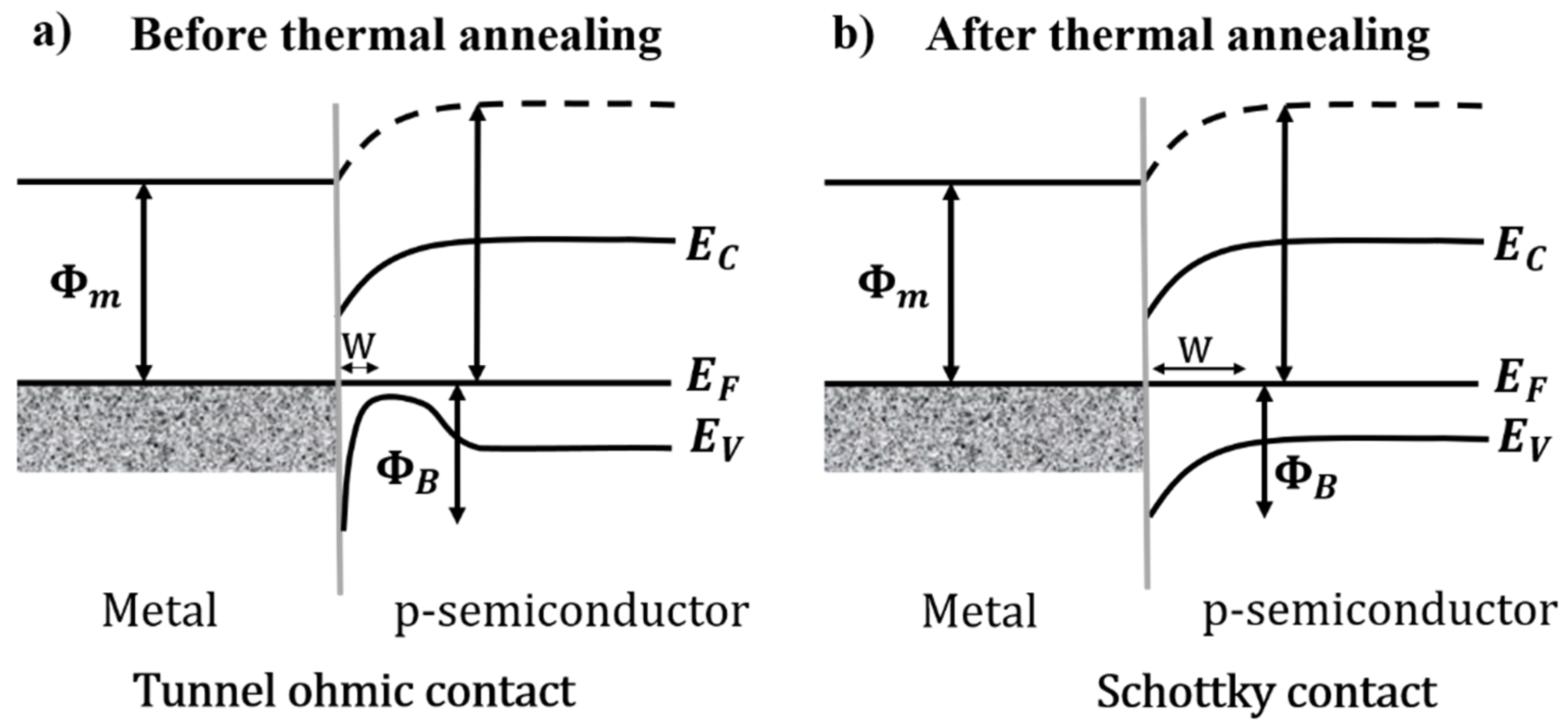
Furthermore, according to the literature, there are two types of contacts for a metal-semiconductor junction: ohmic and rectifier (Schottky) [34,35]. With this in mind, the similarity of the ITO/CdS/PbSe heterojunction with a Schottky diode suggests that the ohmic behavior initially obtained is due to the formation of a tunnel ohmic contact. Figure 8a shows the suggested energy band diagram for this type of contact, which forms a very narrow potential barrier at the interface, thus allowing the electrons to tunnel through the thin barrier [34]. While rectifying behavior was achieved by thermal annealing, this was attributed to better diffusion between the layers of the ITO/CdS/PbSe heterostructure, resulting in well-interlaced interfaces (Figure 8b).
On the other hand, Qiu et al. [20] reported a PbSe-QDs/CdS/CdSe:In/Si heterojunction. They proposed a possible application of their heterojunction as an uncooled midwave infrared device. However, the electrical characterization was limited to dark current density–voltage annealed at various temperatures and the Shockley model was not used to analyze the diode parameters; therefore, their results cannot be comparable with the results of this work. In the same manner, Ling et al. [19] built a PbSe/CdS/nitrogen-doped TiO2 nanorod array photoelectrode. They did not synthesize a homogeneous layer CdS/PbSe heterojunction while they used CdS and PbSe nanoparticles deposited by CVD on TiO2:N nanorods, and their electrical characterization was related to the properties of photoelectrodes; consequently, their results are also not comparable with ours.

4. Conclusions

  • The heterojunction CdS/Pb5(CO3)3O(OH)2 was deposited on glass and glass/ITO substrates via CBD, to which an ion exchange process with selenium ions was applied to obtain the heterojunction CdS/PbSe.
  • The films evolved were uniform and had a good adhesion on the heterostructure ITO/CdS/PbSe, which was characterized by I vs. V, obtaining an ohmic response.
  • Thermal annealing was necessary to improve the diffusion between the layers of the ITO/CdS/PbSe heterostructure and to obtain well-interlaced interfaces, changing from an ohmic to a diode response in the I vs. V characterization.
  • The turn-on voltage and ideality factor under the darkness condition of the diode after thermal annealing were 0.8 V and 2.4, respectively. The ideality factor value may be due to diffusion between ITO/CdS caused by the annealing treatment, which behaved as a MOS hybrid layer, suggesting a Schottky diode response.
  • An ITO/CdS/PbSe device made by aqueous solution methods represents a good, scalable, and promising alternative to produce cost-effective devices.

5. Patents

This research is in the patent process in Mexico under the ID MX/a/2018/008668.

Author Contributions

Conceptualization, J.A.H.-C., R.O.-L. and S.J.C.; methodology, J.A.H.-C., O.S. and R.B.-H.; investigation, J.A.H.-C., O.S., R.B.-H. and S.G.R.-M.; resources, R.O.-L. and S.J.C.; writing—original draft preparation, J.A.H.-C., O.S. and S.G.R.-M.; writing—review and editing, J.A.H.-C., R.B.-H. and S.J.C.; supervision, R.O.-L. and S.J.C. All authors have read and agreed to the published version of the manuscript.

Funding

This research received no external funding.

Institutional Review Board Statement

Not applicable.

Informed Consent Statement

Not applicable.

Data Availability Statement

Data available on request due to privacy/ethical restrictions. The data presented in this study are available on request from the corresponding authors. The data are not publicly available due to their potential to compromise the privacy of research participants.

Acknowledgments

All technicians who operated the characterization equipment.

Conflicts of Interest

The author declares no conflict of interest.

References

  1. Chusnutdinow, S.; Szot, M.; Wojtowicz, T.; Karczewski, G. PbSe/CdTe single quantum well infrared detectors. AIP Adv. 2017, 7, 035111. [Google Scholar] [CrossRef] [Green Version]
  2. He, B.; Ren, Y.X.; Dai, T.J.; Hou, S.; Liu, X.Z. Characterization and performance of graphene-PbSe thin film heterojunction. Rare Metals 2021, 40, 219–224. [Google Scholar] [CrossRef]
  3. Jang, M.H.; Yoo, S.S.; Kramer, M.T.; Dhar, N.K.; Gupta, M.C. Properties of chemical bath deposited and sensitized PbSe thin films for IR detection. Semicond. Sci. Technol. 2019, 34, 115010. [Google Scholar] [CrossRef]
  4. Ren, Y.X.; Dai, T.J.; Luo, W.B.; Liu, X.Z. Evidences of sensitization mechanism for PbSe thin films photoconductor. Vacuum 2018, 149, 190–194. [Google Scholar] [CrossRef]
  5. Sierra, C.; Torquemada, M.C.; Vergara, G.; Rodrigo, M.T.; Gutierrez, C.; Perez, G.; Génova, I.; Catalán, I.; Gómez, L.; Villamayor, V.; et al. Multicolour PbSe sensors for analytical applications. Sens. Actuators B-Chem. 2014, 190, 464–471. [Google Scholar] [CrossRef]
  6. Torquemada, M.C.; Villamayor, V.; Gomez, L.J.; Vergara, G.; Rodrigo, M.T.; Perez, G.; Génova, I.; Catalán, I.; Fernández, D.; Almazán, R.; et al. Monolithic integration of uncooled PbSe bicolor detectors. Sens. Actuators A-Phys. 2013, 199, 297–303. [Google Scholar] [CrossRef]
  7. Caliskan, M.; Yesilkaya, S.S.; Canlica, M. Characteristics of CoPc/CdS hybrid diode device. Bull. Mater. Sci. 2015, 38, 1439–1442. [Google Scholar] [CrossRef] [Green Version]
  8. Hong, C.W.; Shin, S.W.; Suryawanshi, M.P.; Gang, M.G.; Heo, J.; Kim, J.H. Chemically Deposited CdS Buffer/Kesterite Cu2ZnSnS4 Solar Cells: Relationship between CdS Thickness and Device Performance. ACS Appl. Mater. Interfaces 2017, 9, 36733–36744. [Google Scholar] [CrossRef]
  9. Shao, Z.B.; Jie, J.S.; Sun, Z.; Xia, F.F.; Wang, Y.M.; Zhang, X.H.; Ding, K.; Lee, S.-T. MoO3 Nanodots Decorated CdS Nanoribbons for High-Performance, Homojunction Photovoltaic Devices on Flexible Substrates. Nano Lett. 2015, 15, 3590–3596. [Google Scholar] [CrossRef]
  10. Pal, K.; Thomas, S.; Mohan, M. Evaluation of Versatile CdS Nanomaterials Based Liquid Crystals Switchable Device. J. Nanosci. Nanotechnol. 2017, 17, 2401–2412. [Google Scholar] [CrossRef] [PubMed]
  11. He, B.; Xu, J.; Ning, H.P.; Xing, H.Z.; Wang, C.R.; Zhang, X.D.; Mo, G.K.; Shen, X.M. Preparation of nanocrystalline GZO/CdS bilayer films using magnetron sputtering and GZO/CdS/p-Si heterojunction photovoltaic device. J. Infrared Millim. Waves 2019, 38, 44–49. [Google Scholar]
  12. Wu, X.L.; Zhang, D.X.; Cai, H.K.; Zhou, Y.; Ni, J.; Zhang, J.J. Device design of GaSb/CdS thin film thermal photovoltaic solar cells. Acta Phys. Sin. 2015, 64, 096102. [Google Scholar]
  13. Wondmagegn, W.; Mejia, I.; Salas-Villasenor, A.; Stiegler, H.J.; Quevedo-Lopez, M.A.; Pieper, R.J.; Gnade, B. CdS Thin Film Transistor for Inverter and Operational Amplifier Circuit Applications. Microelectron. Eng. 2016, 157, 64–70. [Google Scholar] [CrossRef] [Green Version]
  14. Meza-Arroyo, J.; Reddy, K.C.S.; Rao, M.G.S.; Garibay-Martinez, F.; de Urquijo-Ventura, M.S.; Ramirez-Bon, R. Solution-based CdS thin film transistors with low temperature-processed Al2O3-GPTMS-PMMA as hybrid dielectric gate. Semicond. Sci. Technol. 2021, 36, 045015. [Google Scholar] [CrossRef]
  15. Woollins, J.; Afzaal, M.; O’Brien, P.; Hua, G.; Woollins, J.D. Morphological Evolution of PbSe Crystals via the CVD Route. Chem. Mater. 2010, 22, 4619–4624. [Google Scholar]
  16. Hmood, A.; Kadhim, A.; Abu Hassan, H. Composition-dependent structural and electrical properties of PbSe1−xTex thin films. Superlattices Microstruct. 2012, 51, 825–833. [Google Scholar] [CrossRef]
  17. Huang, N.M.; Basirun, W.J.B.; Yousefi, R.; Jamali-Sheini, F.; Hoomi, S.; Cheraghizade, M.; Basirun, W.J.; Huang, N.M. Large-scale and facile fabrication of PbSe nanostructures by selenization of a Pb sheet. Funct. Mater. Lett. 2015, 8, 1550063. [Google Scholar]
  18. Weng, B.; Qiu, J.; Zhao, L.; Chang, C.; Shi, Z. CdS/PbSe heterojunction for high temperature mid-infrared photovoltaic detector applications. Appl. Phys. Lett. 2014, 104, 121111. [Google Scholar] [CrossRef] [Green Version]
  19. Ling, P.; Zhang, X.; Zhang, Q.; Su, J.; Zhang, X.; Li, J. Chemical vapor deposition of a PbSe/CdS/nitrogen-doped TiO2 nanorod array photoelectrode and its band-edge level structure. New J. Chem. 2012, 36, 2302–2307. [Google Scholar]
  20. Qiu, J.J.; Weng, B.B.; McDowell, L.L.; Shi, Z.S. Low-cost uncooled MWIR PbSe quantum dots photodiodes. RSC Adv. 2019, 9, 42516–42523. [Google Scholar] [CrossRef] [Green Version]
  21. Mohammadi, S.; Zavvari, M. High performance n-ZnO/p-metal-oxides UV detector grown in low-temperature aqueous solution bath. Thin Solid Film. 2017, 626, 173–177. [Google Scholar] [CrossRef]
  22. Yunus, S.H.A.; Sahdan, M.Z.; Kamaruddin, S.A.; Rahim, M.S.; Supee, A.; Ichimura, M. ZnO Growth Properties in ZnO/SnS Heterojunction by a Combination of ECD and CBD Method. In Proceedings of the 2016 World Symposium on Computer Applications & Research (WSCAR), Cairo, Egypt, 12–14 March 2016; pp. 130–133. [Google Scholar]
  23. Terasako, T.; Hambali, N.A.; Jayah, N.A.; Wakisaka, T.; Hashim, A.M.; Yagi, M. Shape controlled growth of ZnO nanorods and fabrication of ZnO/CuO heterojunctions by chemical bath deposition using zinc nitrate hexahydrate and copper (III) nitrate trihydrate. Thin Solid Film. 2015, 596, 201–208. [Google Scholar] [CrossRef]
  24. Mwankemwa, B.S.; Akinkuade, S.; Maabong, K.; Nel, J.M.; Diale, M. Effects of surface morphology on the optical and electrical properties of Schottky diodes of CBD deposited ZnO nanostructures. Phys. B Condens. Matter 2018, 535, 175–180. [Google Scholar] [CrossRef] [Green Version]
  25. Ochoa-Landin, R.; Sastre-Hernandez, J.; Vigil-Galan, O.; Ramirez-Bon, R. Chemically deposited CdS by an ammonia-free process for solar cells window layers. Sol. Energy 2010, 84, 208–214. [Google Scholar] [CrossRef]
  26. Heredia-Cancino, J.A.; Mendivil-Reynoso, T.; Ochoa-Landin, R.; Ramírez-Bon, R.; Castillo, S.J. Optical and structural properties of PbSe films obtained by ionic exchange of lead oxyhydroxicarbonate in a selenium-rongalite solution. Mater. Sci. Semicond. Process. 2016, 56, 90–93. [Google Scholar] [CrossRef]
  27. Luque, A.; Hegedus, S. Handbook of Photovoltaic Science and Engineering; John Wiley & Sons: Hoboken, NJ, USA, 2011. [Google Scholar]
  28. Parker, D.; Singh, D.J. High-temperature thermoelectric performance of heavily doped PbSe. Phys. Rev. B 2010, 82, 035204. [Google Scholar] [CrossRef] [Green Version]
  29. El Kissani, A.; Nkhaili, L.; Ammar, A.; Elassali, K.; Outzourhit, A. Synthesis, annealing, characterization, and electronic properties of thin films of a quaternary semiconductor; copper zinc tin sulfide. Spectrosc. Lett. 2016, 49, 343–347. [Google Scholar] [CrossRef]
  30. Murali, B.; Krupanidhi, S.B. Transport properties of CuIn(1-x)Al(x)Se2/AZnO heterostructure for low cost thin film photovoltaics. Dalton Trans. 2014, 43, 1974–1983. [Google Scholar] [CrossRef]
  31. Begum, A.; Rahman, A. Studies of current–voltage characteristics of nanocrystalline Al/(p)PbSe Schottky barrier junctions. Mater. Sci. Semicond. Process. 2014, 25, 231–237. [Google Scholar] [CrossRef]
  32. Breitenstein, O.; Altermatt, P.; Ramspeck, K.; Schenk, A. The Origin of Ideality factors n > 2 of Shunts and Surfaces in the Dark I-V Curves of Si Solar Cells. In Proceedings of the 21st European Photovoltaic Solar Energy Conference, Dresden, Germany, 4–8 September 2006; pp. 625–628. [Google Scholar]
  33. Chavali, R.V.; Wilcox, J.R.; Ray, B.; Gray, J.L.; Alam, M.A. Correlated Nonideal Effects of Dark and Light I–V Characteristics in a-Si/c-Si Heterojunction Solar Cells. IEEE J. Photovolt. 2014, 4, 763–771. [Google Scholar] [CrossRef] [Green Version]
  34. Roccaforte, F.; La Via, F.; Raineri, V. Ohmic contacts to SiC. Int. J. High Speed Electron. Syst. 2005, 15, 781–820. [Google Scholar] [CrossRef]
  35. DasGupta, N.; DasGupta, A. Semiconductor Devices: Modelling and Technology; PHI Learning Pvt. Ltd.: New Delhi, India, 2004. [Google Scholar]
Figure 1. Scheme of the device based on the ITO/CdS/PbSe heterostructure.
Applsci 11 10914 g001
Figure 2. XRD diffractograms of (a) CdS thin films, and (b) CdS/PbSe.
Applsci 11 10914 g002
Figure 3. The surface morphology of the upper layer of the heterojunction with: (a) and (b) plumbonacrite film, (c) and (d) PbSe film.
Applsci 11 10914 g003
Figure 4. (a) SEM micrograph showing the cross-sectional view of the CdS/Pb5(CO3)3O(OH)2 heterojunction to estimate its thickness, and (b) perspective view of EDS elementary mapping of the CdS/PbSe heterojunction to analyze its elemental composition and their distribution.
Applsci 11 10914 g004
Figure 5. Energy direct bandgap calculated by Tauc procedure for each involved material of the heterojunction: (a) CdS; and (b) PbSe.
Applsci 11 10914 g005
Figure 6. Photograph of ITO/CdS/PbSe heterostructure (real device).
Applsci 11 10914 g006
Figure 7. I vs. V characterization under darkness conditions for the ITO/CdS/PbSe heterostructure: (a) ohmic response (without annealing); and (b) diode response (annealing at 150 °C at 5 min).
Applsci 11 10914 g007
Figure 8. Suggested energy band diagram of the ITO/CdS/PbSe heterojunction as a metal-semiconductor (p-type), (a) before and (b) after thermal annealing, assimilating the ohmic and rectifying electrical response obtained, respectively.
Applsci 11 10914 g008
Table 1. Diode parameters were obtained by fitting the experimental I vs. V curve.
Ideality FactorSaturation Current (eV)Barrier HeightSeries Resistance
ηIs (10−7 mA) Φ B (eV)Rs (Ω)
2.470.361.08712
Publisher’s Note: MDPI stays neutral with regard to jurisdictional claims in published maps and institutional affiliations.