
An Accurate Switching Current Measurement Based on Resistive Shunt Applied to Short Circuit GaN HEMT Characterization


 and
and 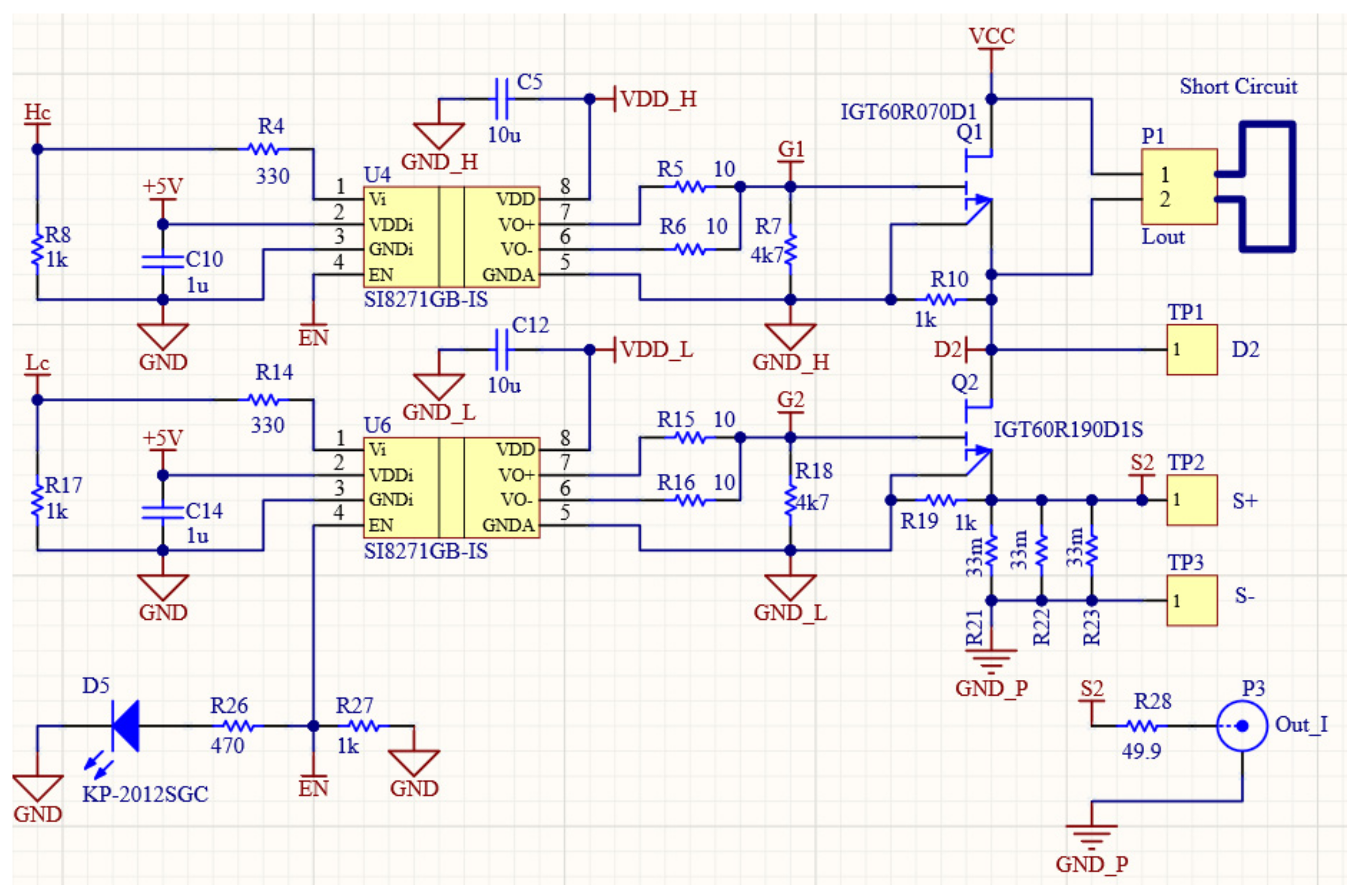
Abstract
:1. Introduction
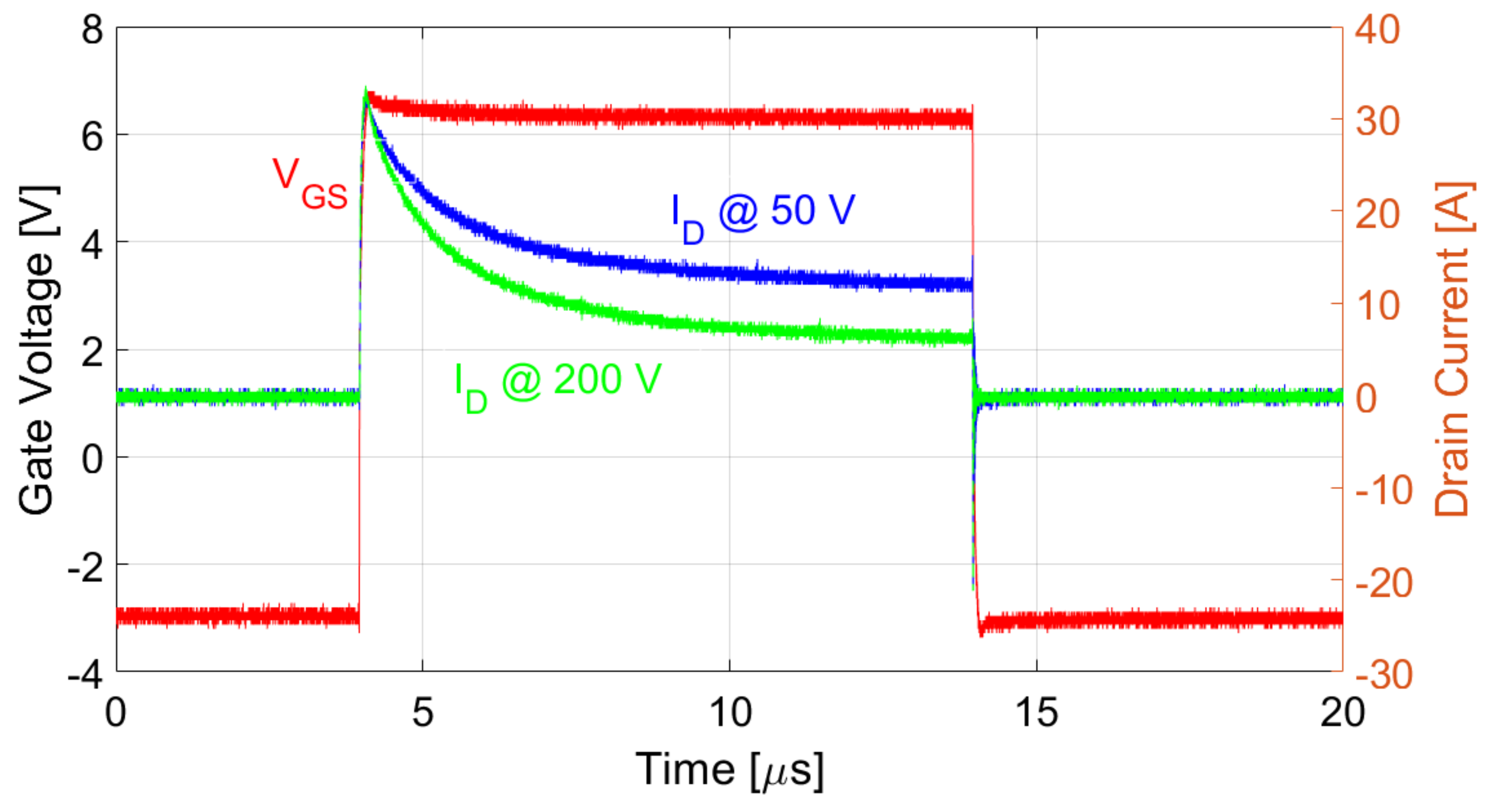
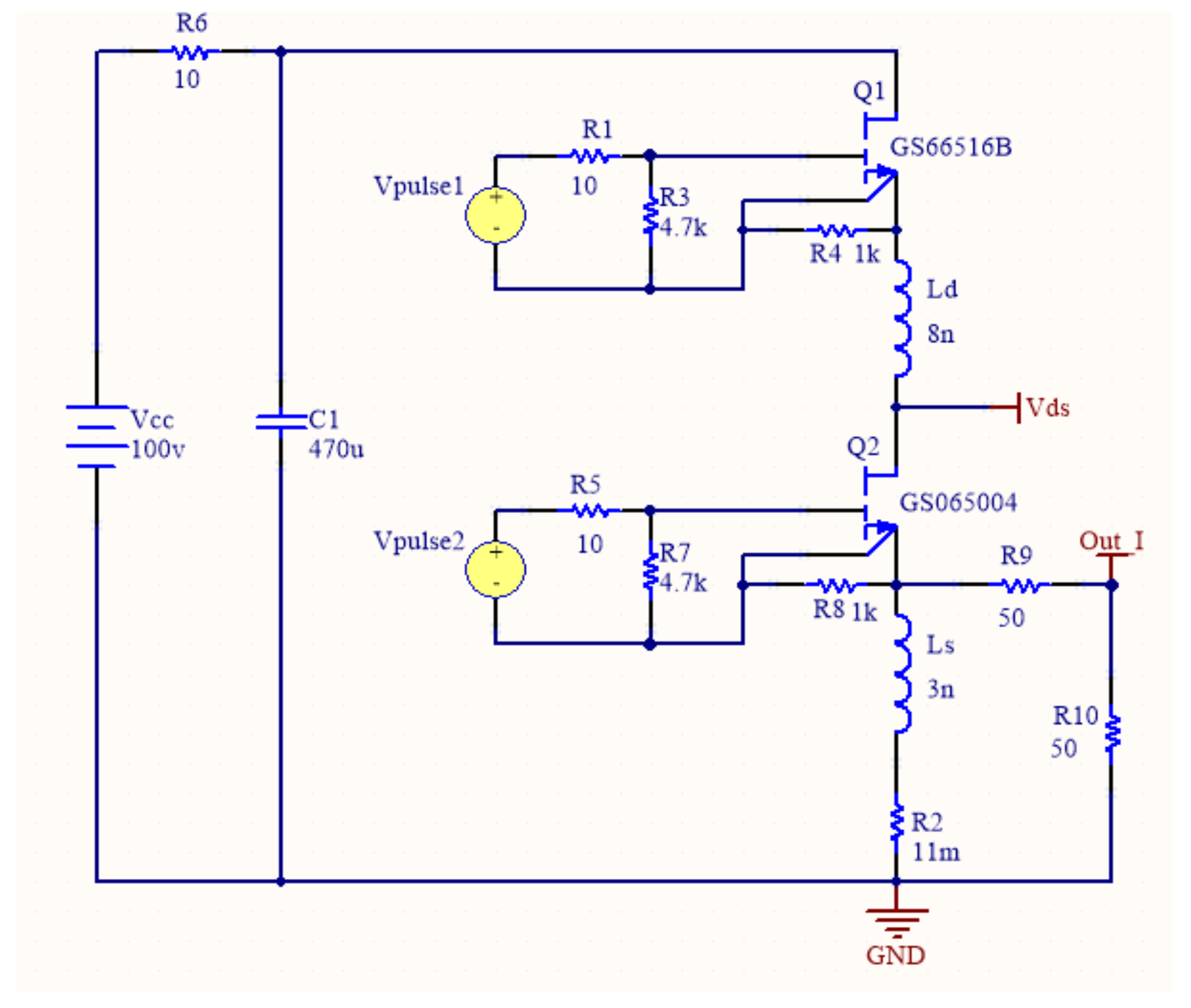
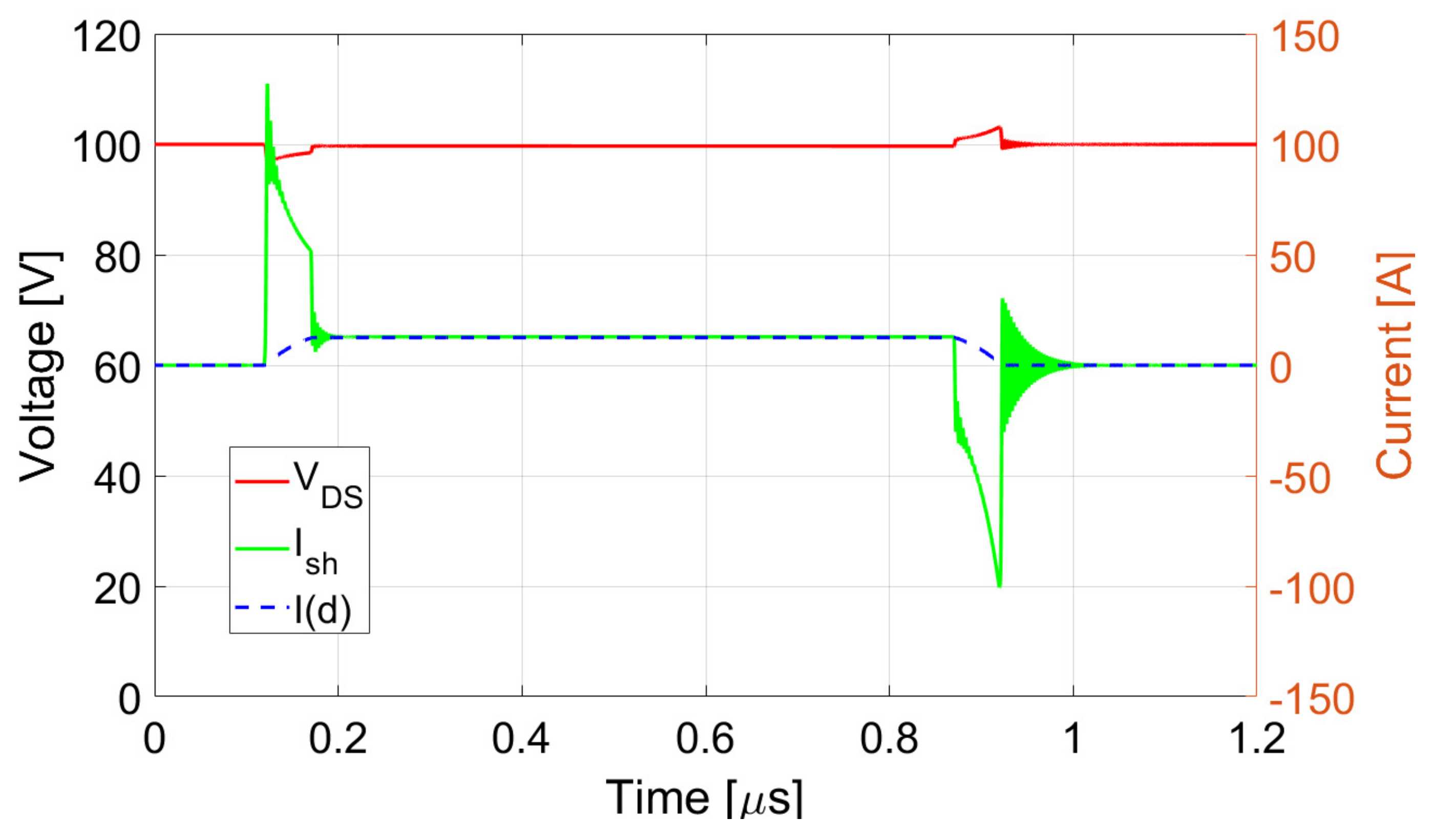
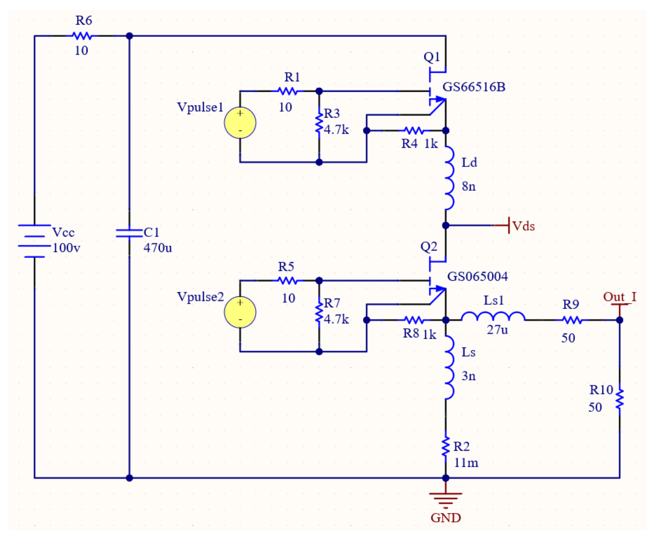
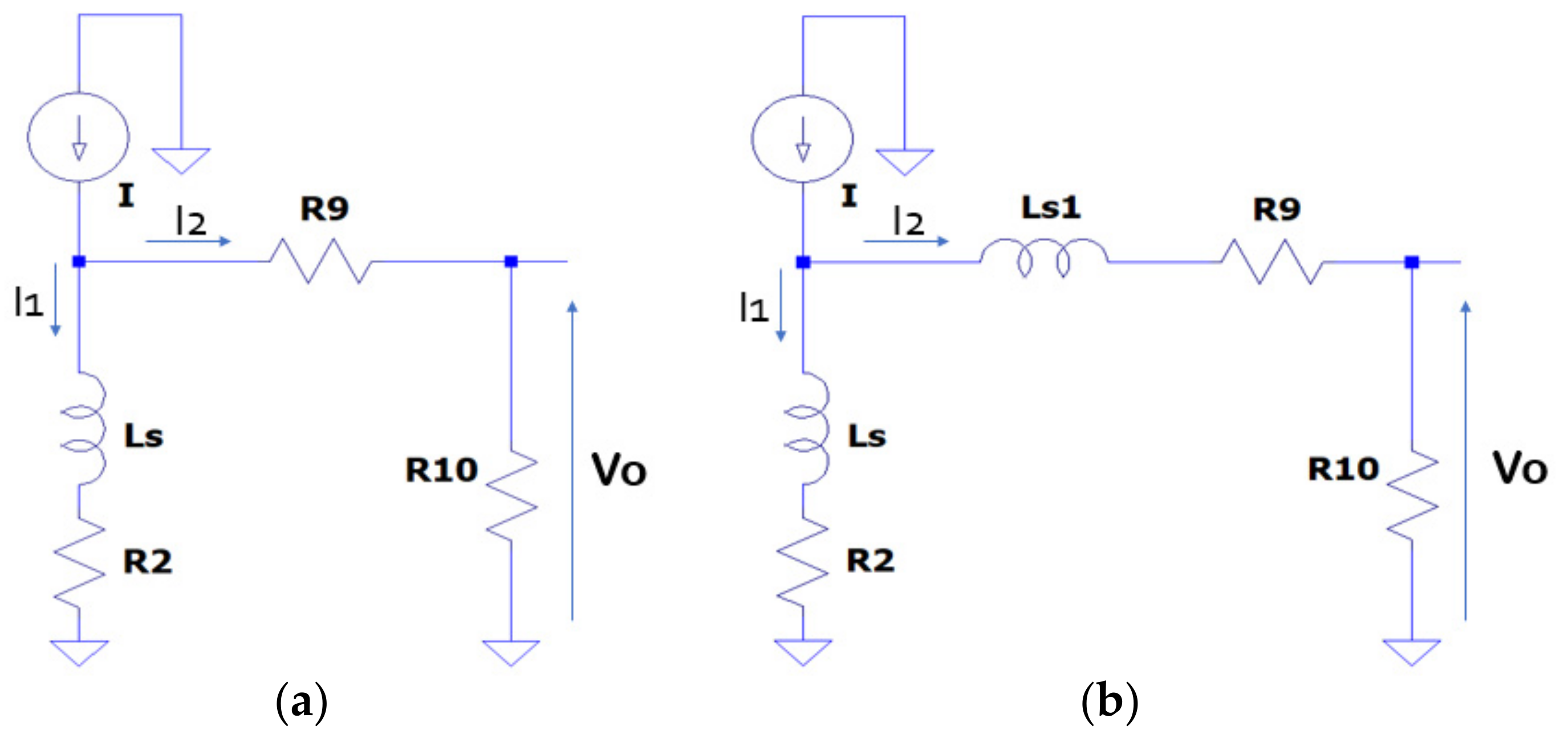
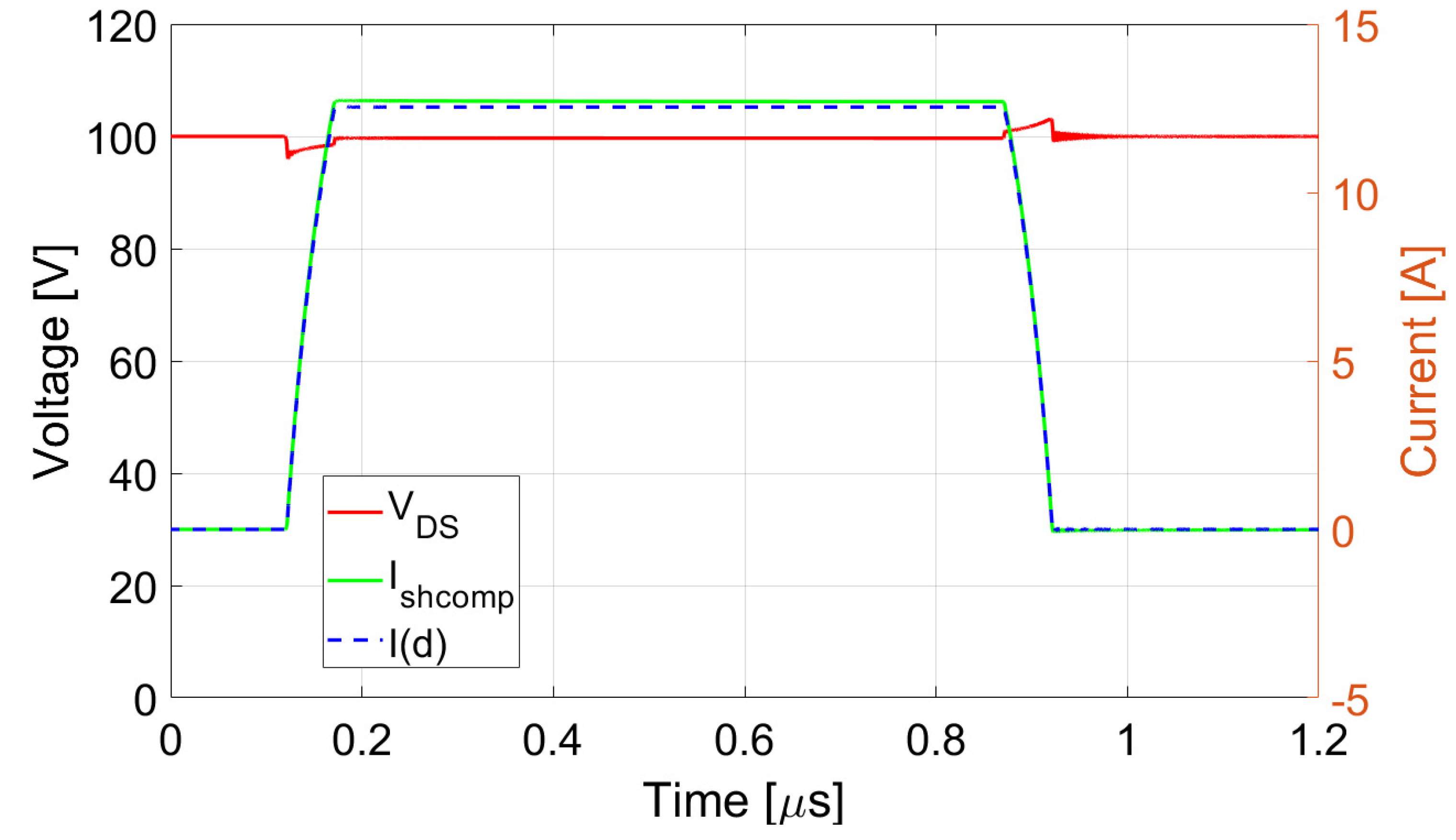
2. Simulations Results
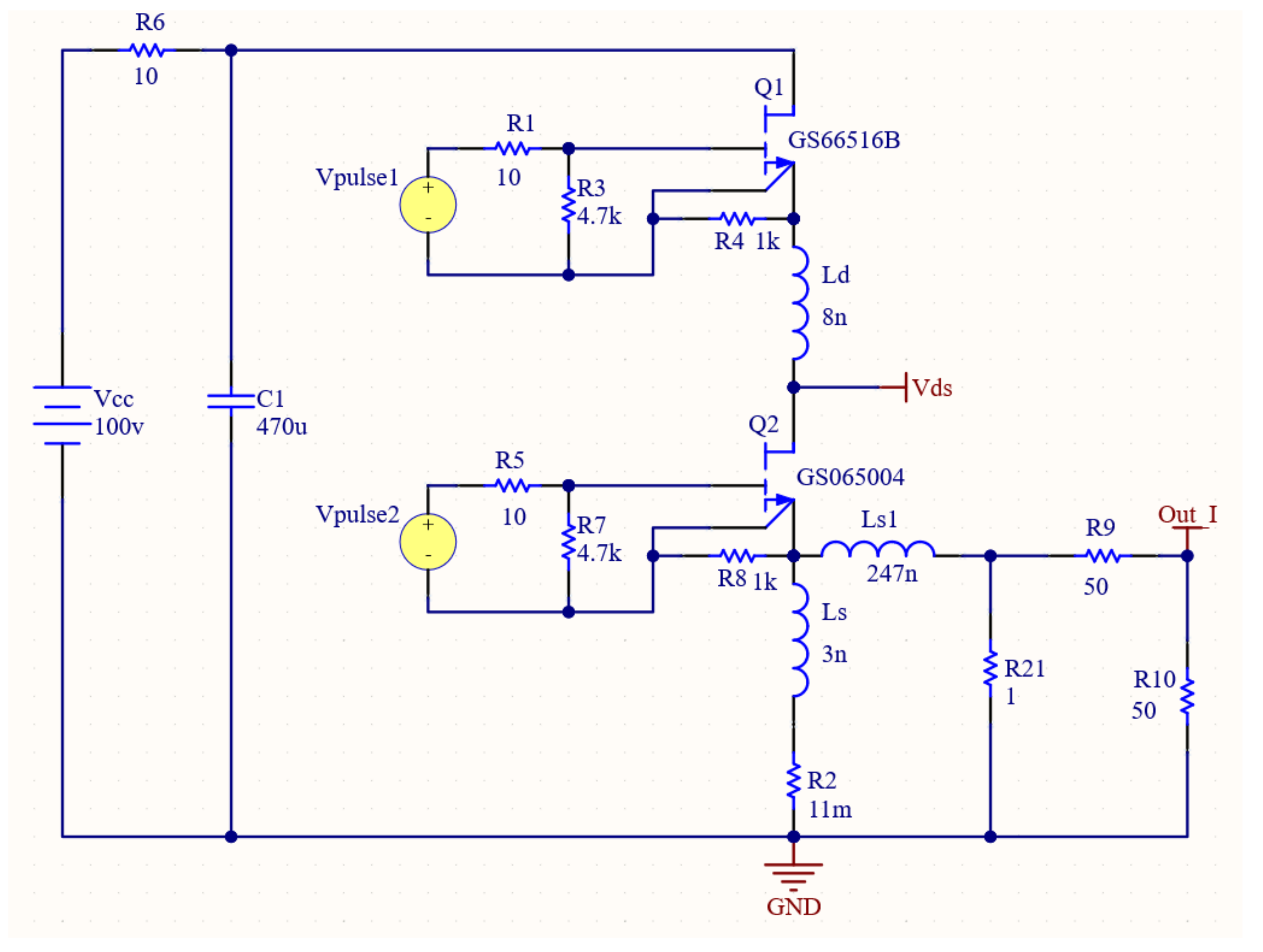
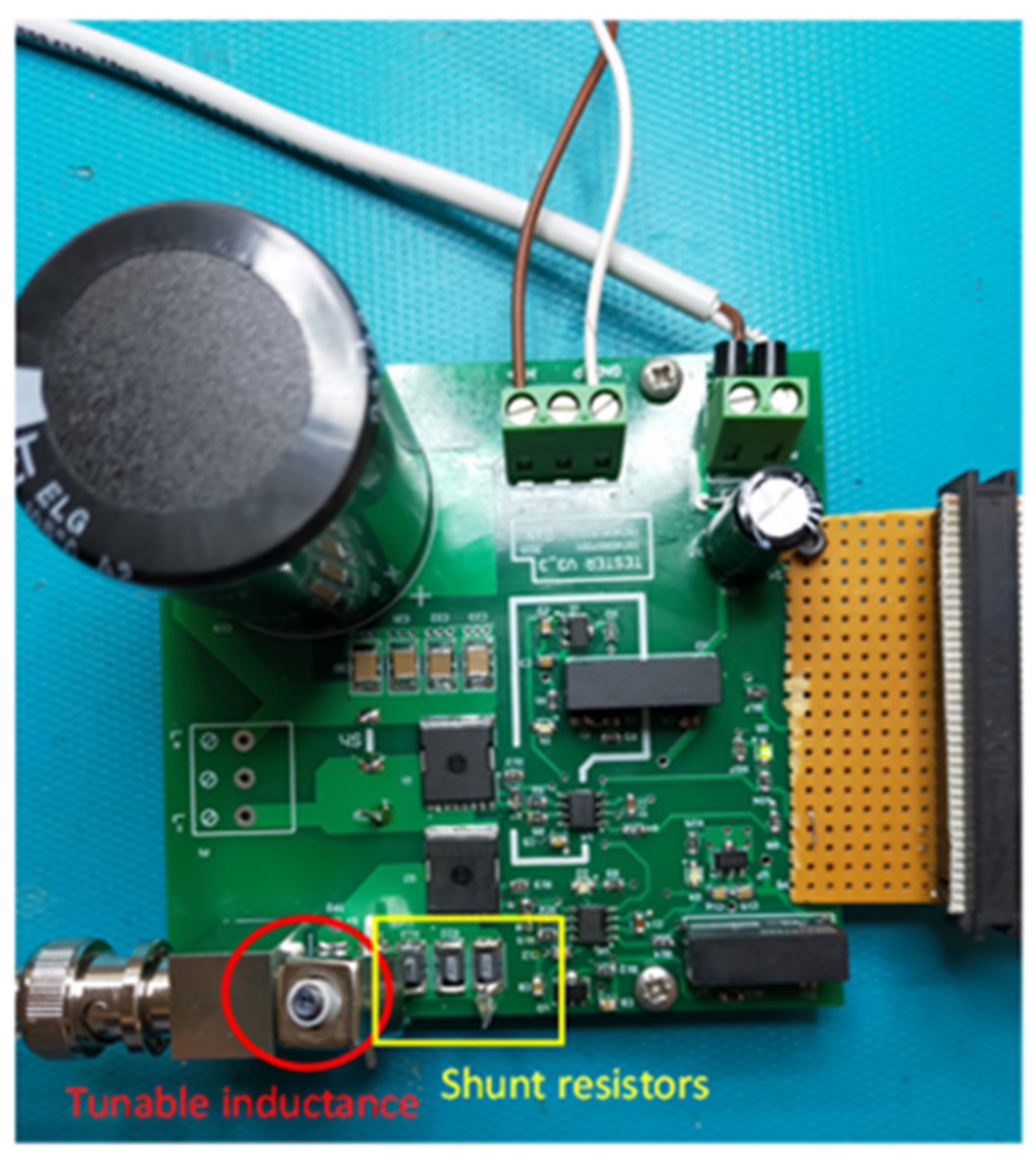
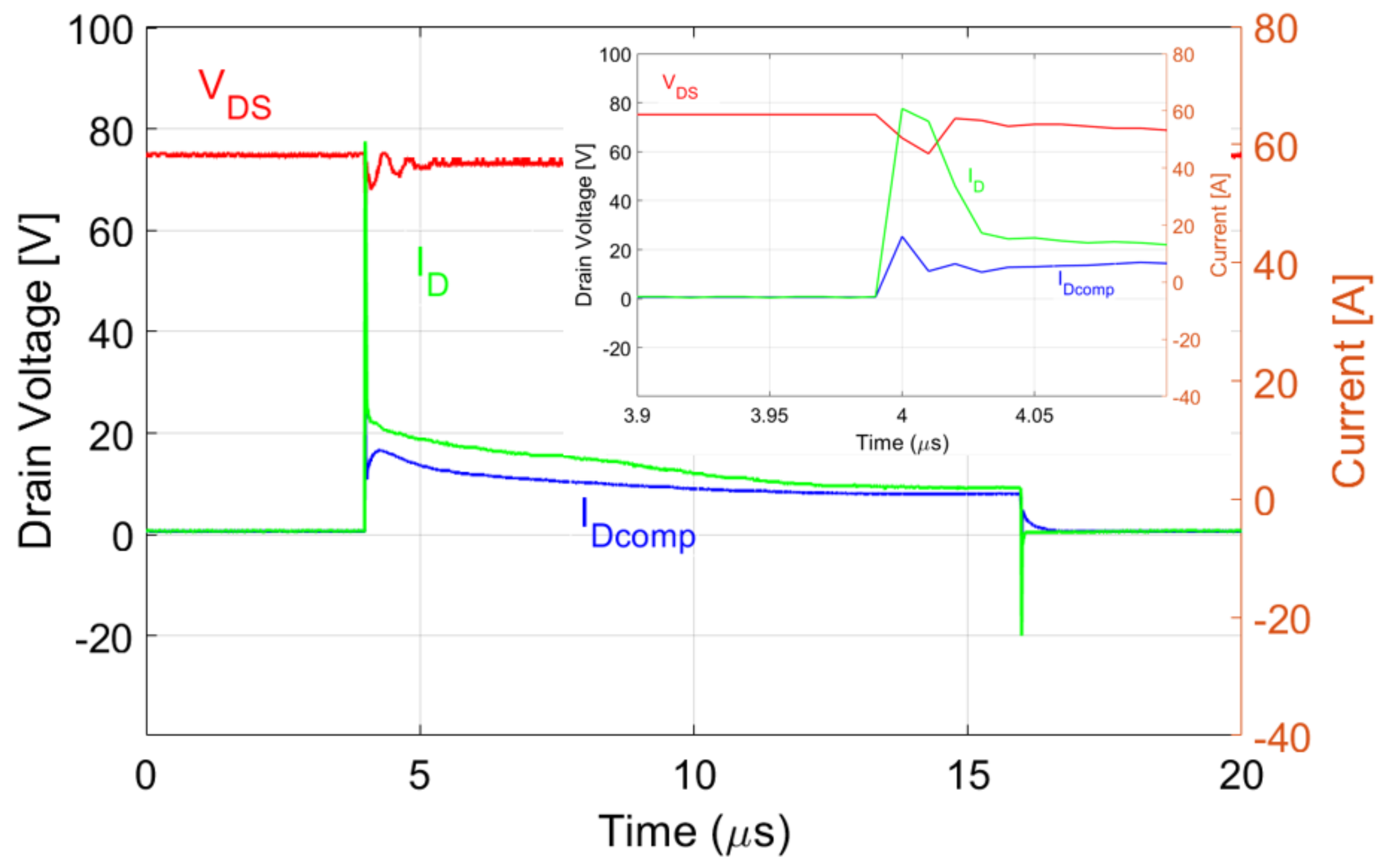
3. Experimental Tests
4. Conclusions
Author Contributions
Funding
Institutional Review Board Statement
Informed Consent Statement
Conflicts of Interest
References
- Satoh, T.; Osawa, K.; Nitta, A. GaN HEMT for Space Applications. In Proceedings of the 2018 IEEE BiCMOS and Compound Semiconductor Integrated Circuits and Technology Symposium (BCICTS), San Diego, CA, USA, 15–17 October 2018; pp. 136–139. [Google Scholar] [CrossRef]
- Boutros, K.S.; Chu, R.; Hughes, B. GaN power electronics for automotive application. In Proceedings of the 2012 IEEE Energytech, Cleveland, OH, USA, 29–31 May 2012; pp. 1–4. [Google Scholar] [CrossRef]
- Longobardi, G.; Efthymiou, L.; Arnold, M. GaN power devices for Electric Vehicles State-of-the-art and future perspective. In Proceedings of the 2018 IEEE International Conference on Electrical Systems for Aircraft, Railway, Ship Propulsion and Road Vehicles & International Transportation Electrification Conference (ESARS-ITEC), Nottingham, UK, 7–9 November 2018; pp. 1–6. [Google Scholar] [CrossRef]
- Shah, F.M.; Xiao, H.M.; Li, R.; Awais, M.; Zhou, G.; Bitew, G.T. Comparative performance evaluation of temperature dependent characteristics and power converter using GaN, SiC and Si power devices. In Proceedings of the 2018 IEEE 12th International Conference on Compatibility, Power Electronics and Power Engineering (CPE-POWERENG 2018), Doha, Qatar, 10–12 April 2018; pp. 1–7. [Google Scholar] [CrossRef]
- Green, B.; Moore, K.; Hill, D.; CdeBaca, M.; Schultz, J. GaN RF device technology and applications, present and future. In Proceedings of the 2013 IEEE Bipolar/BiCMOS Circuits and Technology Meeting (BCTM), Bordeaux, France, 30 September–3 October 2013; pp. 101–106. [Google Scholar] [CrossRef]
- Wang, K.; Yang, X.; Li, H.; Wang, L.; Jain, P. A High-Bandwidth Integrated Current Measurement for Detecting Switching Current of Fast GaN Devices. IEEE Trans. Power Electron. 2018, 33, 6199–6210. [Google Scholar] [CrossRef]
- Allard, B.; Buttay, C.; Joubert, C.; Martin, C.; Mogniotte, J.F.; Morel, H.; Bevilacqua, P.; Le, T.L.; Azzopardi, S. A Study on Shunt Resistor-based Current Measurements for Fast Switching GaN Devices. In Proceedings of the IECON 2019—45th Annual Conference of the IEEE Industrial Electronics Society, Lisbon, Portugal, 14–17 October 2019; pp. 1573–1578. [Google Scholar] [CrossRef] [Green Version]
- Li, H.; Li, X.; Wang, X.; Lyu, X.; Cai, H.; Alsmadi, Y.M.; Liu, L.; Bala, S.; Wang, J. Robustness of 650-V Enhancement-Mode GaN HEMTs Under Various Short-Circuit Conditions. IEEE Trans. Ind. Appl. 2019, 55, 1807–1816. [Google Scholar] [CrossRef]
- Abbate, C.; Busatto, G.; Sanseverino, A.; Tedesco, D.; Velardi, F. Experimental study of the instabilities observed in 650 V enhancement mode GaN HEMT during short circuit. Microelectron. Reliab. 2017, 76–77, 314–320. [Google Scholar] [CrossRef]
- Abbate, C.; Busatto, G.; Sanseverino, A.; Tedesco, D.; Velardi, F. Failure analysis of 650 V enhancement mode GaN HEMT after short circuit tests. Microelectron. Reliab. 2018, 88–90, 677–683. [Google Scholar] [CrossRef]
- Xue, P.; Maresca, L.; Riccio, M.; Breglio, G.; Irace, A. A Comprehensive Investigation on Short-Circuit Oscillation of p-GaN HEMTs. IEEE Trans. Electron. Devices 2020, 67, 4849–4857. [Google Scholar] [CrossRef]
- Sun, J.; Wei, J.; Zheng, Z.; Lyu, G.; Chen, K.J. Distinct Short Circuit Capability of 650-V p-GaN Gate HEMTs under Single and Repetitive Tests. In Proceedings of the 2020 32nd International Symposium on Power Semiconductor Devices and ICs (ISPSD), Vienna, Austria, 13–18 September 2020; pp. 313–316. [Google Scholar] [CrossRef]
- Williford, P.; Wang, F.; Bala, S.; Xu, J. Short Circuit Study of 600 V GaN GITs. In Proceedings of the 2019 IEEE 7th Workshop on Wide Bandgap Power Devices and Applications (WiPDA), Raleigh, NC, USA, 29–31 October 2019; pp. 36–42. [Google Scholar] [CrossRef]
- Bucolo, M.; Buscarino, A.; Famoso, C.; Fortuna, L.; Gagliano, S. Imperfections in Integrated Devices Allow the Emergence of Unexpected Strange Attractors in Electronic Circuits. IEEE Access 2021, 9, 29573–29583. [Google Scholar] [CrossRef]


Publisher’s Note: MDPI stays neutral with regard to jurisdictional claims in published maps and institutional affiliations. |
© 2021 by the authors. Licensee MDPI, Basel, Switzerland. This article is an open access article distributed under the terms and conditions of the Creative Commons Attribution (CC BY) license (https://creativecommons.org/licenses/by/4.0/).
Share and Cite
Abbate, C.; Colella, L.; Di Folco, R.; Busatto, G.; Martano, E.; Palazzo, S.; Sanseverino, A.; Velardi, F. An Accurate Switching Current Measurement Based on Resistive Shunt Applied to Short Circuit GaN HEMT Characterization. Appl. Sci. 2021, 11, 9138. https://doi.org/10.3390/app11199138
Abbate C, Colella L, Di Folco R, Busatto G, Martano E, Palazzo S, Sanseverino A, Velardi F. An Accurate Switching Current Measurement Based on Resistive Shunt Applied to Short Circuit GaN HEMT Characterization. Applied Sciences. 2021; 11(19):9138. https://doi.org/10.3390/app11199138
Chicago/Turabian StyleAbbate, Carmine, Leandro Colella, Roberto Di Folco, Giovanni Busatto, Emanuele Martano, Simone Palazzo, Annunziata Sanseverino, and Francesco Velardi. 2021. "An Accurate Switching Current Measurement Based on Resistive Shunt Applied to Short Circuit GaN HEMT Characterization" Applied Sciences 11, no. 19: 9138. https://doi.org/10.3390/app11199138
APA StyleAbbate, C., Colella, L., Di Folco, R., Busatto, G., Martano, E., Palazzo, S., Sanseverino, A., & Velardi, F. (2021). An Accurate Switching Current Measurement Based on Resistive Shunt Applied to Short Circuit GaN HEMT Characterization. Applied Sciences, 11(19), 9138. https://doi.org/10.3390/app11199138