Article

Effect of Substrate-Thickness on Voltage Responsivity of MEMS-Based ZnO Pyroelectric Infrared Sensors

1
Department of Materials Engineering, National Pingtung University of Science and Technology, Pingtung 912, Taiwan
2
Department of Engineering Science, National Cheng Kung University, Tainan 701, Taiwan
*
Author to whom correspondence should be addressed.
Appl. Sci. 2021, 11(19), 9074; https://doi.org/10.3390/app11199074
Submission received: 3 September 2021 / Revised: 22 September 2021 / Accepted: 26 September 2021 / Published: 29 September 2021
(This article belongs to the Special Issue Advances in MEMS Sensors)

Abstract

:
Pyroelectric infrared sensors incorporating suspended zinc oxide (ZnO) pyroelectric films and thermally insulated silicon substrates are fabricated using conventional MEMS-based thin-film deposition, photolithography, and etching techniques. The responsivity of the pyroelectric films is improved through annealing at a temperature of 500 °C for 4 h. The temperature variation and voltage responsivity of the fabricated sensors are evaluated numerically and experimentally for substrate thickness in the range of 1 to 500 μm. The results show that the temperature variation and voltage responsivity both increase with a reducing substrate thickness. For the lowest film thickness of 1 μm, the sensor achieves a voltage sensitivity of 3880 mV/mW at a cutoff frequency of 400 Hz. In general, the results presented in this study provide a useful source of reference for the further development of MEMS-based pyroelectric infrared sensors.

1. Introduction

Pyroelectric infrared sensors, consisting of a thin film of ferroelectric crystal material sandwiched between two electrodes, produce an electrical voltage (or current) in response to temperature variation and have found widespread use in recent years for many applications, including thermal comfort monitoring, infrared light detection and imaging, fire detection, intruder alarms, body temperature monitoring, and so on [1,2,3,4,5,6,7,8,9,10]. Many studies have reported that the sensitivity of pyroelectric sensors can be improved by reducing heat losses from the sensing elements to the supporting substrate or environment [11,12,13,14,15]. It has been shown that this can be readily achieved by using bulk micromachining techniques to realize freestanding sensing structures, such as floating membranes, cantilever beams and bridges, which are effectively suspended above the supporting silicon substrate and shielded from the environment [16]. Moreover, pyroelectric sensors can be easily integrated with modern IC circuits on the same chip to realize sophisticated system-on-chip (SoC) devices for a wide variety of sensing and detection applications [17,18].
Hashimoto et al. [19] constructed a people-counting system based on a pyroelectric array detector for detecting the moving direction and number of passersby at a door. The pyroelectric detector incorporated a thin PbTiO3 bulk ceramic film with a thickness of approximately 40 μm and was driven by a supply voltage of 5 V. The detector showed a maximum voltage sensitivity of 23 mV/mW at a chopping frequency of 10 Hz. Chang and Tang [20] fabricated an integrated pyroelectric sensor consisting of a PZT thin film and a Si JFET. The device was characterized over a modulation frequency range of 0.2 to 10 Hz and was found to have a voltage sensitivity of 191 mV/mW at a modulation frequency of 1 Hz when implemented with a 500 μm thick silicon substrate. Some other ferroelectric ceramics (e.g., (Bi, Na)TiO3, (Sr, Ba)NbO3, Pb(Sc, Ta)O3 (Ba, Sr)TiO3 and Pb(Zr, Sn, Ti)O3) were investigated to be suitable for pyroelectric detection applications, recently [21]. Lienhard and Heepmann [22] investigated the transmittance of thin nickel (Ni) films deposited on pyroelectric polyvinylidene fluoride (PVDF) films over the infrared spectral range of 2–50 μm. It was shown that the absorbance characteristics of the pyroelectric sensor could be effectively controlled through an appropriate specification of the Ni film thickness. Chong et al. [23] fabricated a thin-film pyroelectric sensor array consisting of 16 sensing elements made of metal–ZnO–metal sandwiched layers with dimensions of 200 μm × 200 μm. The sensor response was enhanced by depositing the sensing elements on a thermally isolated and freestanding Si3N4/SiO2 membrane created by removing the underside of the SiO2 substrate using a conventional back-etching technique. The experimental results showed that the device achieved a maximum voltage sensitivity of 110 mV/mW at a cutoff frequency of 20 Hz. Hsiao et al. [24] used a two-step radio frequency (RF) sputtering technique to fabricate a ZnO pyroelectric sensor on a back-etched silicon wafer. The use of the two-step deposition process was found to produce a ZnO film with a preferred c-axis orientation and an enhanced voltage response. It was shown that the sensor achieved a maximum voltage sensitivity of 8.6 mV/mW at a cutoff frequency of 500 Hz when implemented with a Ni coating on the uncovered part of the ZnO film in order to enhance the absorption of the incident energy. Wei et al. [25] fabricated ZnO pyroelectric sensors with partially covered and fully covered electrodes, respectively. The experimental results showed that the responsivity of the partially covered device was around four times higher than that of the fully covered device for incident light frequencies in the range of 10–1000 Hz. Liu et al. [26] deposited a thin Ni layer on the surface of a PZT pyroelectric sensor as both the top electrode and a selective absorption layer. The maximum absorption coefficient of the resulting sensor was found to be 0.8 at a wavelength of 0.664 μm and 0.7 at a wavelength of 4 μm. Gaur et al. [27] presented a pyroelectric detector consisting of a polycrystalline AlN thin film and a SiO2 layer with a thickness of 1.0 μm which served as both a thermal isolation layer and a diaphragm to support the sensor. It was shown that the absorptivity of the device could be enhanced by sputtering an additional Au film with a thickness of 160 nm on top of the AlN layer. Overall, the characterization results showed that the device achieved a response time of 8.0 ms and a pyroelectric current responsivity of 2.5 × 10⁻⁶ A/W.
Recently, Luo et al. [28] proposed a method to leverage the synergy between location and motion information to realize human simultaneous tracking and activity recognition by constructing a wireless sensor network and the sensor nodes of pyroelectric infrared sensor arrays. Yan et al. [29] examined various factors influencing human identification based on pyroelectric infrared sensor. They found that distance, human target, sensor design, body type, human moving velocity, and signal modulation mask are all important factors in the mechanism. Wu et al. [30] presented pyroelectric detection and sensing signal processing algorithms to create a non-wearable cooperative indoor human localization system based on pyroelectric sensor networks.
While the studies above provide many useful insights into the design, fabrication and characterization of pyroelectric sensors fabricated with various metallic layers, the effects of the substrate thickness on the performance of pyroelectric sensors have thus far attracted only little attention in the literature. Accordingly, the present study fabricates pyroelectric sensors consisting of suspended zinc oxide (ZnO) pyroelectric films with substrate thicknesses ranging from 1 to 500 μm supported on thermally insulated back-etched silicon substrates. The temperature variation and voltage response of the various sensors are evaluated numerically and experimentally for an infrared laser source with a power of 10 mW and a wavelength of 765 nm. In general, the results show that the performance of the proposed sensor improves as the thickness of the substrate reduces.

2. Principles and Designs

The analysis of any pyroelectric detector requires a careful consideration of both its thermal characteristics and its electrical response. Assume that infrared light with a power W(t) sinusoidally modulated at a frequency ω is incident on the surface of a pyroelectric sensing element with an electrode area A, thickness d and surrounding temperature T. The incident power can be formulated mathematically as follows [31]:
W t = W 0 e i w t
Assume further that the sensing element has a thermal capacity HT, and the thermal conductance to the surroundings is denoted as GT, giving a thermal time constant of τ T = H T ÷ G T . Given an emissivity η , the temperature difference between the element and its surroundings, θ , can be described as [28]:
η W t = H T d θ d t + G T θ
which has the solution [31]:
θ = η W 0 e i e t G T + i ω H T
Differentiating Equation (3), the rate of the temperature difference between the element and its surrounding is obtained as:
d θ d t = ω η W 0 G T 1 + ω 2 τ T 2 1 2
Quantitatively, the pyroelectric effect can be evaluated as the product of the pyroelectric coefficient p of the sensing material and the rate of change of the temperature difference, i.e.,
Δ P s = p × Δ θ
When the top surface of a thin-film pyroelectric sensor is exposed to a heat source, the resulting temperature variation in the pyroelectric film manifests itself as a release of charge at the surface of the material and the subsequent production of a small voltage. Assuming that the pyroelectric coefficient p of the sensing element has a component p in the direction perpendicular to the electrode surface (with area A), the resulting charge can be detected as a current, i p 
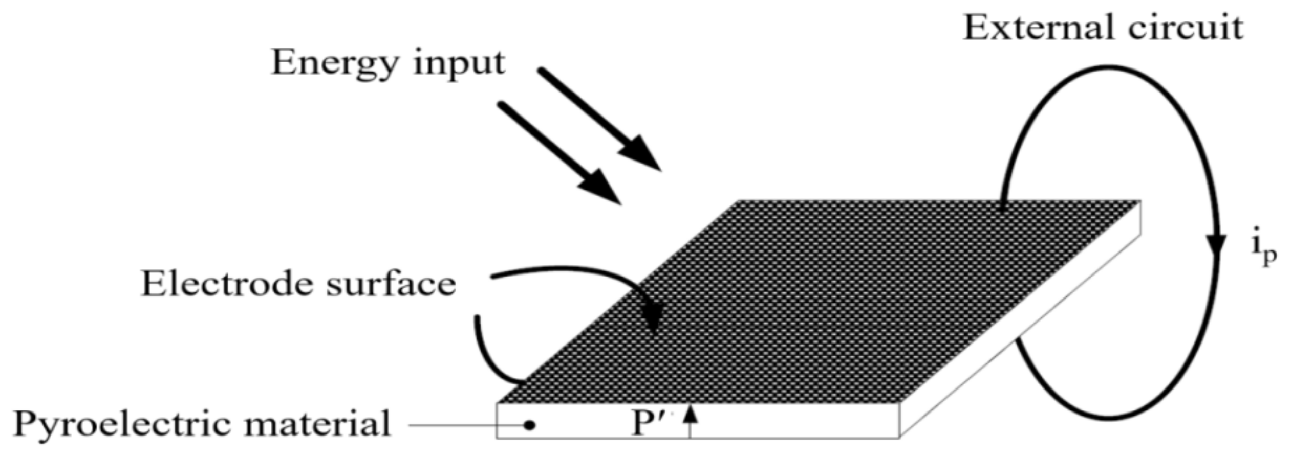
, flowing through the external circuit (see Figure 1). The magnitude of this charge is given by [31] as:
i p = A × d P S d t = A × p × d θ d t
In other words, the sensor is “AC coupled” to any input energy flux which generates a change in temperature, where this input may take the form of either electromagnetic radiation absorbed in the pyroelectric material or heat generated by the reaction of chemical species on a suitable catalyst deposited on the element surface.
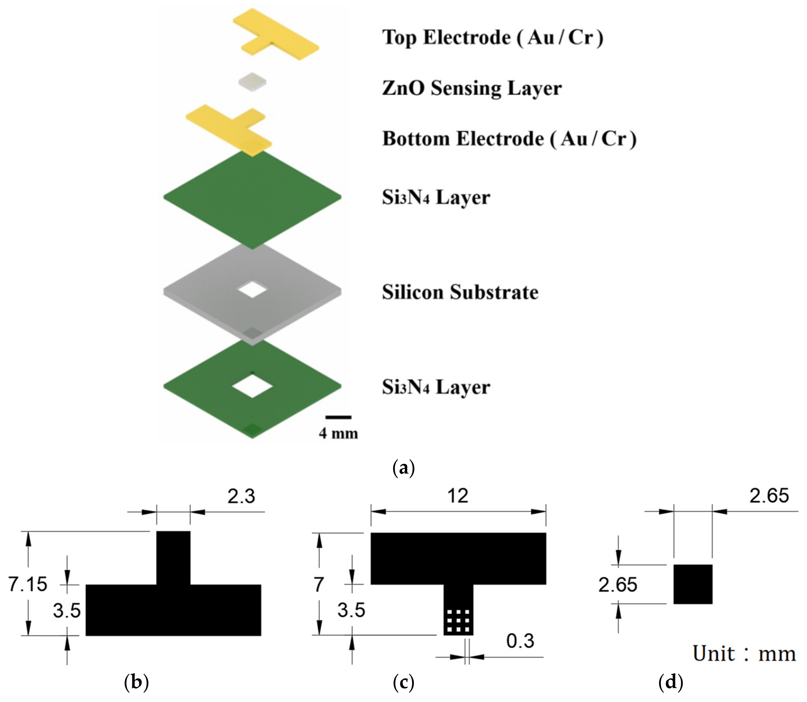
Figure 2 illustrates the basic structure and dimensions of the ZnO thin-film pyroelectric sensor considered in the present study. From Equation (6), it can be seen that a higher temperature variation rate in the ZnO layer leads to a higher response current. Moreover, a partially covered top electrode yields a greater responsivity than a fully covered electrode since the uncovered part of the ZnO sensing element is directly exposed to the heat source and, therefore, experiences a larger heat absorption. Intuitively, a larger covered top electrode area reduces the temperature variation rate in the ZnO layer. By contrast, a larger uncovered top electrode area increases the temperature variation rate but decreases the responsivity since the resulting smaller top electrode area has a reduced ability to hold electric charge. Consequently, as shown in Figure 2c, the ZnO pyroelectric sensor considered in the present study was designed with a mesh-type partially covered top electrode in order to achieve a trade-off between the temperature variation rate and the charge storage ability of the electrode.

3. Methods and Fabrication

The performance of the proposed ZnO sensor was evaluated both numerically and experimentally. The details of the simulation process and fabrication procedure are described in the following.

3.1. Simulation Method

In general, the temperature variation rate in the pyroelectric layer has a significant effect on the responsivity of the sensor. In particular, a higher temperature variation yields an improved electrical response and varies in accordance with the substrate thickness.
Intuitively, reducing the thickness of the substrate enhances the temperature variation within it and, therefore, increases the magnitude of the induced electrical charge. Accordingly, the study commenced by performing ANSYS FLUENT simulations based on a simple two-dimensional finite element model to examine the rate of thermal conduction in ZnO pyroelectric sensors with substrate thicknesses of 1, 100, 200, 300, 400, and 500 μm, respectively (see Figure 3).
In performing the simulations, symmetric boundary conditions were imposed on the lateral sides of the model and the diode laser used to illuminate the sensor was assumed to have a power of approximately 10 mW and a wavelength of 765 nm.

3.2. Fabrication

Figure 4 presents a schematic illustration showing the basic steps in the MEMS process used to fabricate the ZnO pyroelectric devices. As shown, the multilayer sensor was supported on a silicon wafer with both sides polished. Si3N4 thin films with a thickness of 1 μm were deposited on either side of the wafer using a low-pressure chemical vapor deposition (LPCVD) process to serve as electrical insulation layers (see Figure 4a). An Au/Cr bottom electrode was patterned on the substrate by electron beam evaporation and wet etching, as shown in Figure 4b–d. Note that the Cr layer (thickness 300 Å) was deposited first as an intermediary layer to improve the adhesion between the gold layer (thickness 1000 Å) and the substrate. The ZnO sensing layer was sputtered on the lower electrode/substrate using a ZnO target with a purity of 99.99% (see Figure 4e). Note that the ZnO target was pre-sputtered for 30 min prior to the deposition process in order to remove any surface impurities. In addition, the chamber was pumped to a base pressure of 5 × 10⁻⁶ Torr before sputtering. The chamber was then supplied with argon gas at a rate of 30 sccm to maintain a constant chamber pressure of 5 × 10⁻³ Torr during the deposition process. The sputtering process was performed with an RF power of 150 W for 2 h. The substrate was heated at a temperature of 220 °C throughout the deposition process in order to improve the microstructural quality of the ZnO film. Following the sputtering process, the ZnO sensing layer was patterned by photolithography and wet etching with an HNO3:H2O (1:4) etchant (see Figure 4f,g).
A Au/Cr electrode was patterned on the ZnO sensing layer using a similar process to that used for the bottom electrode, with the exception of a lift-off patterning process (see Figure 4h–j). Finally, the sensing layer on the suspended structure was released by etching the underside Si3N4 layer with CF4 25 sccm and O2 5 sccm at a power of 50 W for 8 min (see Figure 4k) and then wet etching the silicon substrate with KOH 30 wt. % at 80 °C at a rate of 1.5 μm/min (see Figure 4l).

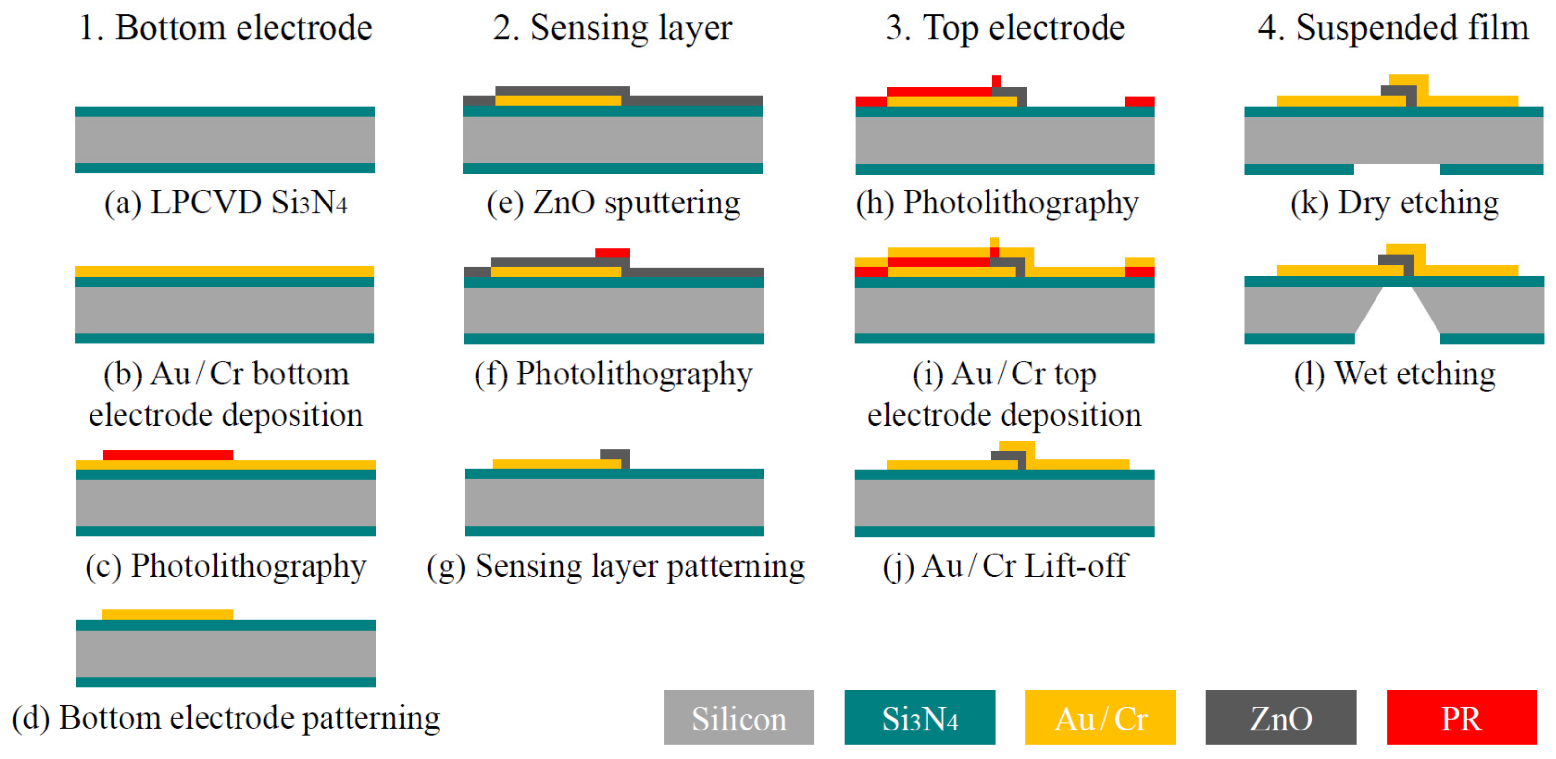
4. Results and Discussion

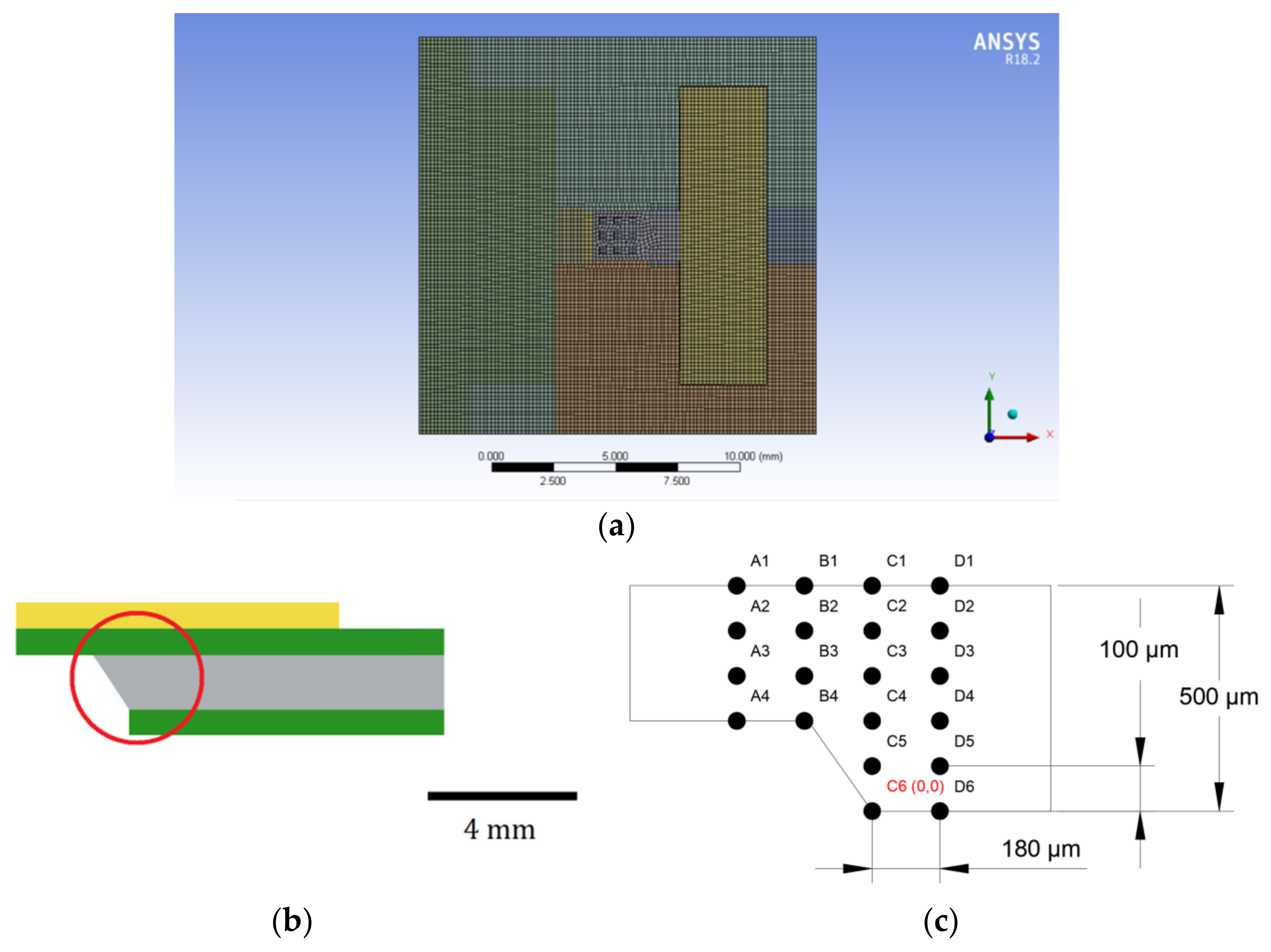
For the pyroelectric sensor considered in the present study, the output voltage scales proportionally with the temperature variation within the ZnO layer. Hence, the study commenced by performing COMSOL FLUENT simulations to determine the temperature variation at each of the node points shown in Figure 3c.
Figure 5 shows the corresponding results obtained for the temperature variation at node point A1 given five different thicknesses of substrate (i.e., 100, 200, 300, 400 and 500 μm, respectively). Note that the boundary condition for the temperature is set as 36.5 °C in every case. The results show that the rate of change of the temperature at point A1 increases with a decreasing substrate thickness. In other words, as the thickness of the substrate reduces, the time required to reach steady-state temperature conditions also decreases.
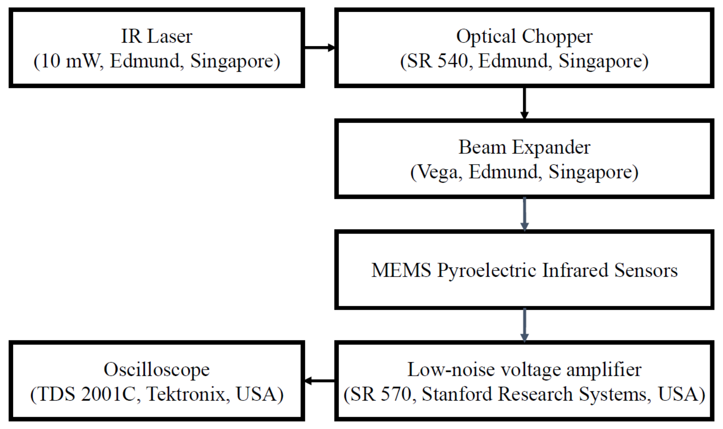
An experimental responsivity measurement system was established to further evaluate the performance of the ZnO pyroelectric sensors (see Figure 6). The radiation source had the form of a calibrated infrared (IR) laser with a maximum power of 10 mW and a wavelength of 765 nm. The laser beam was chopped and molded as a wave with a modulated frequency of w by an optical chopper and was then expanded by a beam expander such that the beam spot diameter had a size of 3 mm and thus covered the entire region of the patterned top electrode of the sensor. In performing the experiments, the distance between the infrared source and the sensing layer was set as 15 cm unless specified otherwise, and the output voltage of the sensor was amplified using an SR570 low-noise voltage amplifier. Finally, the output signal of the sensor was displayed and recorded using a digital oscilloscope.
For ZnO pyroelectric material, there exists a strong relation between the intensity of the (002) crystal peak and the responsivity of the pyroelectric sensor, where a higher value of the crystal peak indicates a higher quality of the crystal structure. In order to investigate the crystal orientation of the present ZnO sensing layer, ZnO films with a thickness of 889 nm were deposited on silicon substrates in an argon atmosphere with an RF sputtering power of 150 W and a working pressure of 5 × 10⁻³ Torr. The films were then annealed at various temperatures in the range of 300 to 600 °C for 4 h. The structures of the annealed films were characterized by X-ray power diffraction with a scanning angle of 30–60°; an operating voltage and current of 40 kV and 40 mA, respectively, and Cu Kα1 radiation ( λ = 0.154 nm). For each film, the sampling interval angle was set as 0.03° and the sampling time was 0.45 s.
Figure 7 shows that XRD patterns of the ZnO films annealed at temperatures of 300, 400, 500 and 600 °C, respectively. For reference purposes, the figure also shows the XRD pattern of an as-deposited (non-annealed) film. It is seen that the intensity of the (002) peak increases as the annealing temperature is increased to 500 °C, but then decreases as the temperature is further increased to 600 °C.
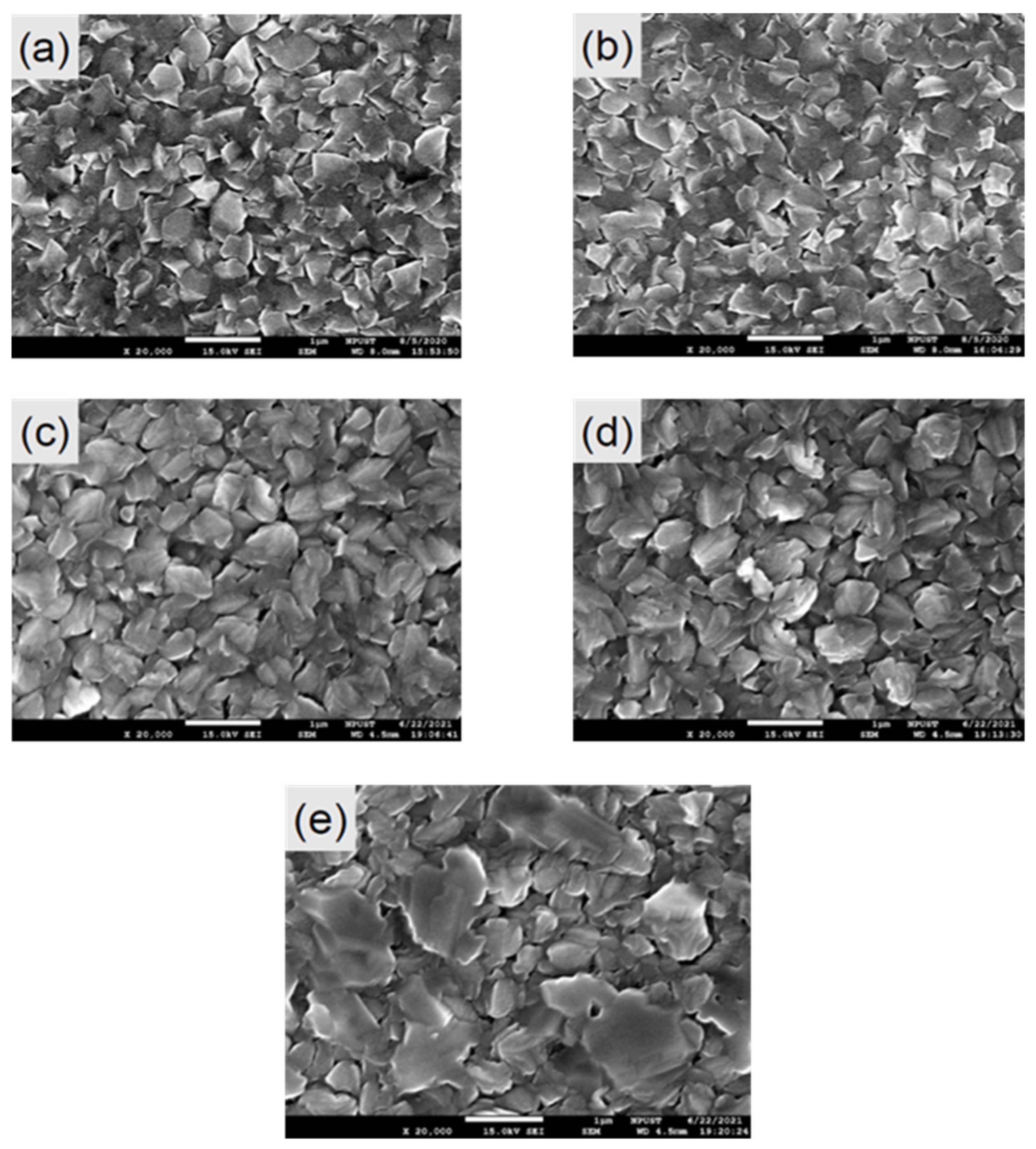
Figure 8 presents top-view SEM micrographs of the ZnO films shown in Figure 7. As shown in Figure 8a, the non-annealed sample has a flaky surface morphology with a small crystal size. For the sample annealed at 300 °C, the crystal size increases as a result of grain growth (Figure 8b). As the annealing temperature is increased to 400 °C, the ZnO grain size continues to increase. However, some pores are evident in the crystal structure (Figure 8c). For the sample annealed at 500 °C, the ZnO grain size increases once again. Moreover, the crystal structure is more dense, and fewer voids are observed (Figure 8d). Finally, at an annealing temperature of 600 °C, the ZnO grain size continues to increase and the crystal structure becomes even more dense (Figure 8e). Overall, the results presented in Figure 8 show that both the grain size and the densification of the ZnO film increase with an increasing annealing temperature. As a result, the thermal conduction performance of the ZnO sensing layer improves, leading to an enhanced sensing performance. However, despite the better grain growth at 600 °C (see Figure 8e), the XRD results presented in Figure 7 show that the intensity of the (002) peak at 600 °C is lower than that at 500 °C. Thus, the optimal annealing temperature was determined to be 500 °C.
The element composition of the ZnO film annealed at 500 °C was examined by energy-dispersive X-ray spectroscopy (EDS). The corresponding results are presented in Figure 9 and show that the film consists of 22.39 wt. % O and 77.61 wt. % Zn. Notably, the stoichiometry ratio of Zn to O is not 1:1 since the annealing environment is not oxygen free and hence the content of O atoms is slightly increased.
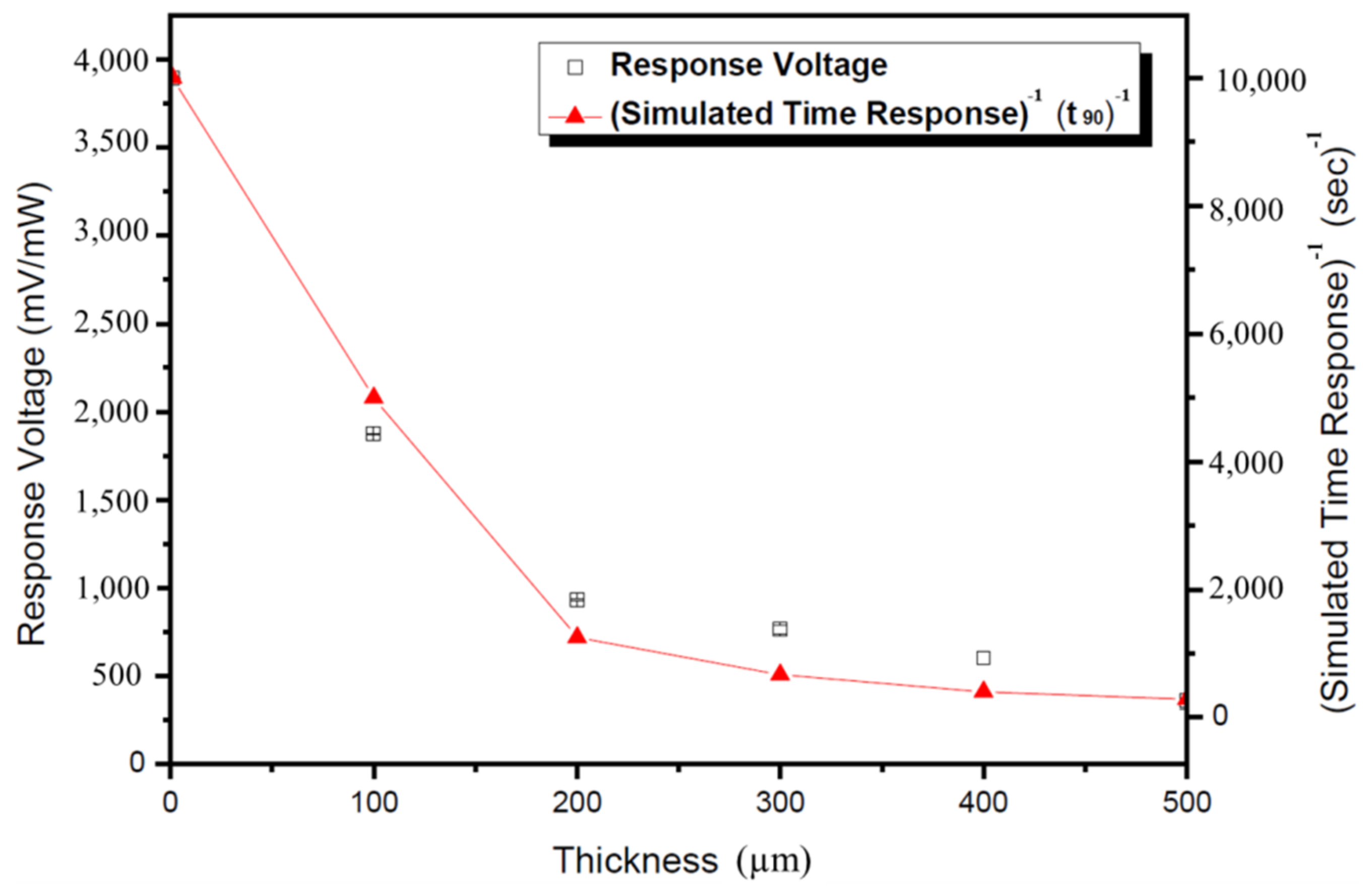
Figure 10 shows the experimental results obtained for the voltage responsivities of the ZnO pyroelectric sensors with different substrate thicknesses of 1, 100, 200, 300, 400, and 500 μm, respectively, at cutoff frequencies in the range of 0–3500 Hz. For comparison purposes, the responsivity of a packaged sensor is also shown. Note that the voltage responsivity is defined here as the ratio of the output voltage of the sensor to the input power of the incident heat source. As expected, the voltage responsivity increases with a reducing substrate thickness as a result of the greater temperature variation within the ZnO film. From inspection, the maximum voltage sensitivity is equal to 3800 mV/mW and is obtained for a substrate thickness of 1 μm and a cutoff frequency of 400 Hz. It is noted that the packaged sensor has a low voltage responsivity of just 3100 mV/mW due to connection losses and internal resistance losses, respectively.
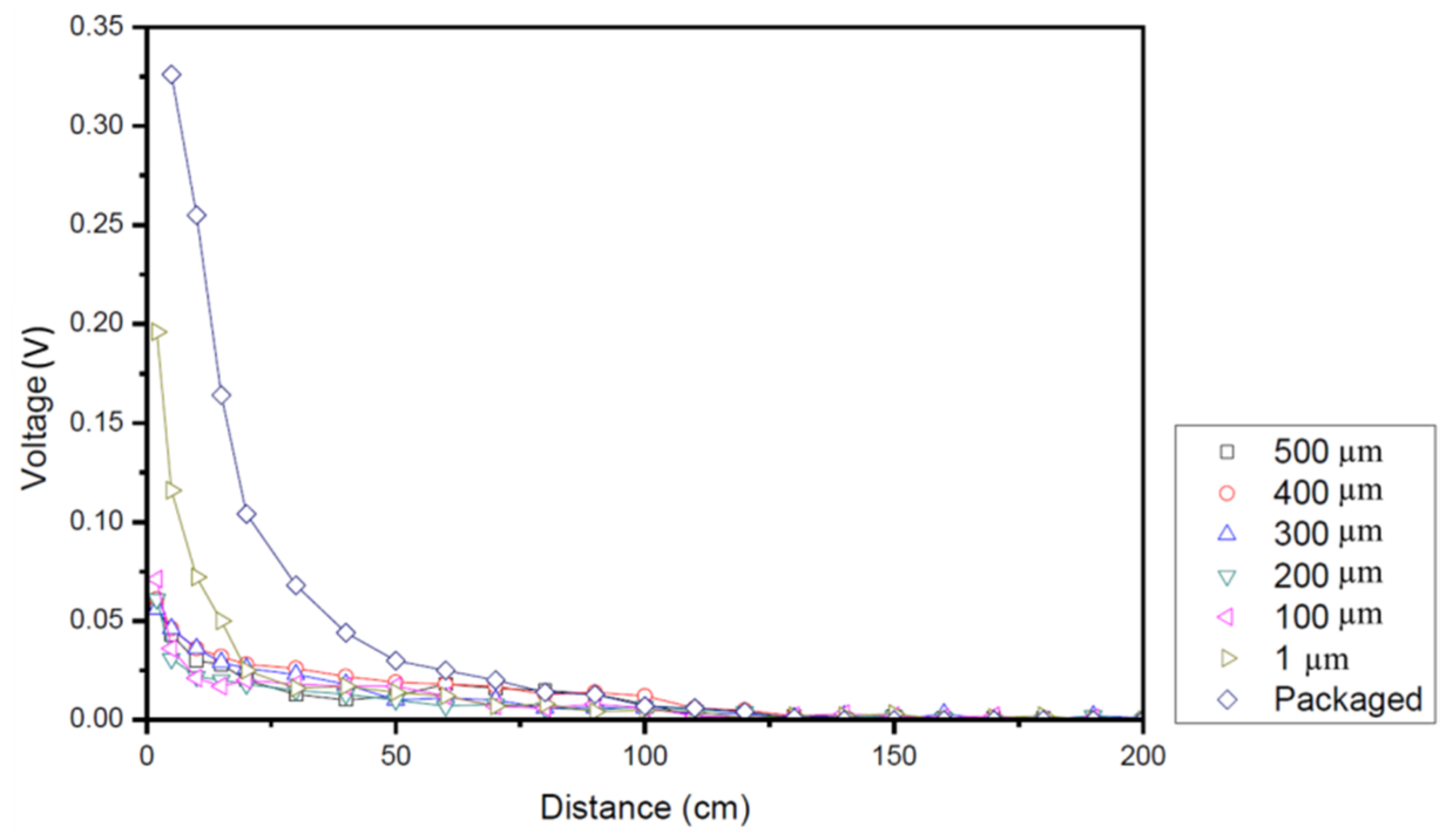
Figure 11 shows the output voltages of the various sensors at a cutoff frequency of 400 Hz for various distances of the sensor from the infrared power source in the range of 0–200 cm. For distances of less than 100 cm, the packaged sensor provides the highest voltage output among all the sensors. However, the sensor with a ZnO thickness of 1 μm also provides a reasonable response at sensing distances less than approximately 25 cm. For all of the sensors, the output voltage reduces to zero as the sensing distance increases beyond 100 cm.
Figure 12 shows the experimental results obtained for the output voltages of the various sensors at a cutoff frequency of 400 Hz and the simulation results obtained for the temperature variation within the corresponding sensing layers. In general, a good agreement is observed between the two sets of results, thereby confirming the validity of Equation (6) in Section 2.

5. Conclusions

Pyroelectric sensors are finding application in an increasing range of fields nowadays. However, the effects of the substrate thickness on the voltage response of these sensors have thus far attracted relatively little attention in the literature. Consequently, the present study has fabricated ZnO-based pyroelectric sensors with various substrate thicknesses in the range of 1–500 μm and has characterized the performance of these sensors using both simulation and experimental methods. In general, the results have shown that the temperature variation within the substrate increases with a reducing thickness and gives rise to a higher output voltage as a result. The maximum voltage responsivity is equal to 3800 mV/mW and is obtained using a substrate thickness of 1 μm and a cutoff frequency of 400 Hz. For all of the sensors, the output voltage reduces to zero as the sensing distance increases beyond 100 cm. In general, the results presented in this study provide a useful source of reference for the further development of pyroelectric sensors with an enhanced performance in various fields.

Author Contributions

Conceptualization and design, L.-M.F. and C.-Y.L.; methodology and simulation, C.-X.Y. and K.-Y.L.; fabrication and experiments, C.-X.Y. and K.-Y.L.; data analysis, L.-M.F. and C.-Y.L., writing, C.-X.Y., L.-M.F. and C.-Y.L. All authors have read and agreed to the published version of the manuscript.

Funding

This research was funded by the Ministry of Science and Technology in Taiwan, grant number MOST 110-2622-E-020-001; MOST 109-2622-E-006-009-CC2, and MOST 109-2221-E-006-043-MY3.

Institutional Review Board Statement

Not applicable.

Informed Consent Statement

Not applicable.

Data Availability Statement

The data presented in this study are available on request from the corresponding author.

Conflicts of Interest

The authors declare no conflict of interest.

References

  1. Fanger, P.O. Thermal Comfort: Analysis and Applications in Environmental Engineering, 3rd ed.; Danish Technical Press: Copenhagen, Denmark, 1970; pp. 193–195. [Google Scholar]
  2. Thermal Environmental Conditions for Human Occupancy; ANSI/ASHRAE Standard; ASHRAE: Atlanta, GA, USA, 1981; Volume 55.
  3. Moderate Thermal Environments-Determination of the PMV and PPD Indices and Specification of the Conditions for Thermal Comfort; International Standard ISO 7730:1984(E); ISO: Geneva, Switzerland, 1984.
  4. Ploss, B.; Bauer, S. Characterization of materials for integrated pyroelectric sensors. Sens. Actuator A Phys. 1991, 26, 407–411. [Google Scholar] [CrossRef]
  5. Hammes, P.C.A.; Regtien, P.P.L. An integrated infrared sensor using the pyroelectric polymer PVDF. Sens. Actuator A Phys. 1992, 32, 396–402. [Google Scholar] [CrossRef]
  6. Lienhard, D.; Nitschke, S.; Ploss, B.; Ruppl, W. The optimization of low cost integrated pyroelectric sensor arrays. Sens. Actuator A Phys. 1994, 41–42, 553–557. [Google Scholar] [CrossRef]
  7. Togami, Y.; Okuyama, M.; Hamakawa, Y. Pyroelectric infrared image sensors using Si CCD and FET arrays. Sens. Actuator A Phys. 1994, 40, 111–116. [Google Scholar] [CrossRef]
  8. Porter, S.G. A brief guide to pyroelectric detectors. Ferroelectrics 1981, 33, 193–216. [Google Scholar] [CrossRef]
  9. Liu, S.T.; Long, D. Pyroelectric detectors and materials. IEEE 1978, 66, 14–26. [Google Scholar] [CrossRef]
  10. Watton, R. Ferroelectric materials and devices in infrared detection and imaging. Ferroelectric 1987, 91, 87–108. [Google Scholar] [CrossRef]
  11. Oden, P.I.; Wachter, E.A.; Thundat, T.; Warmack, R.J. Optical and infrared detection using microcantilevers. SPIE 1966, 2744, 345–354. [Google Scholar]
  12. Kohil, M.; Wuethrich, C.; Brooks, K.; Willing, B.; Forster, M.; Mmuralt, P.; Setter, N.; Ryser, P. Pyroelectric thin-film sensor array. Sens. Actuator A Phys. 1997, 60, 147–153. [Google Scholar] [CrossRef]
  13. Ye, C.P.; Tamagawa, T.; Polla, D.L. Experimental studies on primary and secondary pyroelectric effects in Pb(Zrx, Ti1-x)O3, PbTiO3, and ZnO thin films. J. Appl. Phys. 1991, 70, 5538–5543. [Google Scholar] [CrossRef]
  14. Setiadi, D.; Regtien, P.P.L. A VDF/TrFE copolymer on silicon pyroelectric sensor: Design considerations and experiments. Sens. Actuator A Phys. 1995, 47, 408–412. [Google Scholar] [CrossRef] [Green Version]
  15. Ko, J.S.; Liu, W.; Zhu, W. Substrate effects on the properties of pyroelectric thin film IR detector. Sens. Actuator A Phys. 2001, 93, 117–122. [Google Scholar] [CrossRef]
  16. Dillner, U. Thermal Simulation and Realization of Micromachined Thermal Sensor Arrays. In Proceedings of the 5th NEXUSPAN Workshop on Thermal Aspects in Microsystem Technology, Budapest, Hungary, 6–8 May 1998; pp. 133–141. [Google Scholar]
  17. Takayama, R.; Tomita, Y.; Iijima, K.; Ueda, I. Pyroelectric properties and application to infrared sensors of PbTiO3, PbLaTiO3, and PbZrTiO3 ferroelectric thin films. Ferroelectrics 1991, 118, 325–342. [Google Scholar] [CrossRef]
  18. Choi, J.R.; Polla, D. Integration of microsensors in GaAs MESFET process. J. Micromech. Microeng. 1993, 3, 60–64. [Google Scholar] [CrossRef]
  19. Hashimoto, K.; Yoshinomoto, M.; Matsueda, S.; Morinaka, K.; Yoshiike, N. Development of people-counting system with human-information sensor using multi-element pyroelectric infrared array detector. Sens. Actuator A Phys. 1997, 58, 165–171. [Google Scholar] [CrossRef]
  20. Chang, C.C.; Tang, C.S. An integrated pyroelectric infrared sensor with a PZT thin film. Sens. Actuator A Phys. 1998, 65, 171–174. [Google Scholar] [CrossRef]
  21. Liu, Z.; Lu, T.; Dong, X.; Wang, G.; Liu, Y. Ferroelectric ceramics for pyroelectric detection applications: A review. IEEE Trans. Ultrason. Ferroelectr. Freq. Control 2021, 68, 242–252. [Google Scholar] [CrossRef]
  22. Lienhard, D.; Heepmann, F.; Ploss, B. Thin nickel films as absorbers in pyroelectric sensor arrays. Microelectron 1995, 29, 101–104. [Google Scholar] [CrossRef]
  23. Chong, N.; Chan, H.L.W.; Choy, C.L. Pyroelectric sensor array for in-line monitoring of infrared laser. Sens. Actuator A Phys. 2002, 96, 231–238. [Google Scholar] [CrossRef]
  24. Hsiao, C.C.; Huang, K.Y.; Hu, Y.C. Fabrication of a ZnO Pyroelectric Sensor. Sensors 2008, 8, 185–192. [Google Scholar] [CrossRef] [Green Version]
  25. Wei, C.S.; Lin, Y.Y.; Hi, Y.C.; Wu, C.W.; Shih, C.W.; Huang, C.T.; Chang, S.H. Partial-electroded ZnO pyroelectric sensors for responsivity improvement. Sens. Actuator A Phys. 2006, 128, 18–24. [Google Scholar] [CrossRef]
  26. Liu, W.; Ko, J.; Zhu, W. Influences of thin Ni layer on the electrical and absorption properties of PZT thin film pyroelectric IR sensors. Infrared Phys. Technol. 2000, 41, 169–173. [Google Scholar] [CrossRef]
  27. Gaur, S.P.; Rangra, K.; Kumar, D. MEMS AlN pyroelectric infrared dector with medium to long wave IR absorber. Sens. Actuator A Phys. 2019, 300, 111660. [Google Scholar] [CrossRef]
  28. Luo, X.; Guan, Q.; Tan, H.; Gao, L.; Wang, Z.; Lio, X. Simultaneous indoor tracking and activity recognition using pyroelectric infrared sensors. Sensors 2017, 8, 1738. [Google Scholar] [CrossRef]
  29. Yan, J.; Lou, P.; Li, R.; Hu, J.; Xiong, J. Research on the multiple factors influencing human identification based on pyroelectric infrared sensors. Sensors 2018, 18, 604. [Google Scholar] [CrossRef] [Green Version]
  30. Wu, C.M.; Chen, X.Y.; Wen, C.Y.; Sethares, W.A. Cooperative networked PIR detection system for indoor human localization. Sensors 2021, 21, 6180. [Google Scholar] [CrossRef]
  31. Whatmore, R.W. Pyroelectric devices and materials. Rep. Prog. Phys. 1986, 49, 1335–1386. [Google Scholar] [CrossRef]
Figure 1. Principle of pyroelectric effect [31].
Applsci 11 09074 g001
Figure 2. Designs of MEMS-based pyroelectric infrared sensors: (a) structural arrangement of sensor, and dimensions of (b) bottom electrode, (c) top electrode and (d) sensing layer.
Applsci 11 09074 g002
Figure 3. (a) Mesh, (b) location and (c) distribution of analyzed points in the simulation model of suspended sensing structure.
Applsci 11 09074 g003
Figure 4. Schematic illustration showing main steps in fabrication process of pyroelectric infrared sensor: (a) LPCVD deposition of Si3N4, (b) E-beam deposition of Au/Cr bottom electrode, (c) photolithography, (d) patterning of bottom electrode by wet etching, (e) RF sputter deposition of ZnO thin film, (f) photolithography, (g) patterning of sensing layer by wet etching, (h) photolithography, (i) E-beam deposition of Au/Cr top electrode, (j) lift-off, (k) dry etching of back Si3N4 layer, and (l) KOH wet etching of silicon substrate.
Applsci 11 09074 g004
Figure 5. Simulated temperature variation at point A1 of the sensing layer for different substrate thicknesses (100, 200, 300, 400 and 500 μm) and a temperature boundary condition of 36.5 °C.
Applsci 11 09074 g005
Figure 6. Experimental setup for evaluating voltage response of ZnO pyroelectric sensors.
Applsci 11 09074 g006
Figure 7. XRD patterns of as-deposited ZnO film and ZnO films annealed at temperatures in the range of 300–600 °C.
Applsci 11 09074 g007
Figure 8. SEM micrographs showing sub-micrometer grain size of ZnO thin films annealed at different temperatures: (a) non-annealed, (b) 300 °C, (c) 400 °C, (d) 500 °C and (e) 600 °C.
Applsci 11 09074 g008
Figure 9. EDS analysis results of sputtered ZnO.
Applsci 11 09074 g009
Figure 10. Voltage responsivity of sensors with substrate thicknesses of 1, 100, 200, 300, 400 and 500 μm and cutoff frequencies in the range of 0–3500 Hz.
Applsci 11 09074 g010
Figure 11. Voltage response of different sensors located at distances of 0–200 cm from infrared power source. Note that the cutoff frequency is equal to 400 Hz in every case.
Applsci 11 09074 g011
Figure 12. Comparison of experimental voltage response and simulated temperature variation for ZnO sensors with different substrate thicknesses. (Note that the cutoff frequency is 400 Hz in every case.)
Applsci 11 09074 g012
Publisher’s Note: MDPI stays neutral with regard to jurisdictional claims in published maps and institutional affiliations.

