Article

High Vacuum Packaging of MEMS Devices Containing Heterogeneous Discrete Components

1
Department of Electronics, Peking University, Beijing 100871, China
2
Zhongkeqidi Optoelectronic Technology (Guangzhou) Co., Ltd., Guangzhou 510700, China
*
Author to whom correspondence should be addressed.
Appl. Sci. 2021, 11(18), 8536; https://doi.org/10.3390/app11188536
Submission received: 23 July 2021 / Revised: 10 September 2021 / Accepted: 12 September 2021 / Published: 14 September 2021
(This article belongs to the Section Applied Physics General)

Abstract

:

Featured Application

A systematic method for high vacuum packaging of MEMS devices is proposed in this paper. It is applicable to many kinds of MEMS devices such as sensors, gyroscopes and actuators to reduce power consumption and improve their performance.

Abstract

Vacuum packaging of Micro-electro-mechanical system (MEMS) devices is a hot topic for its advantages of improving performance and reducing power consumption. In this paper, the physics package of a chip scale atomic clock (CSAC), as a typical kind of MEMS device, is performed by vacuum packaging based on a systematic method proposed by us. The whole process, including low outgassing and thermal stable materials selection, prebaking for desorption, getter firing for absorption and solder reflow for vacuum sealing is introduced thoroughly. The thermogravimetric analysis or thermal gravimetric analysis (TGA) is used to analyze the thermal stability and desorption of materials. The leak rate of physics packages is measured to be less than 4 × 10⁻¹⁰ Pa·m3/s by helium leak detection. The residual gas pressure and composition in physics packages are analyzed after vacuum packaging. The results show a high vacuum ~0.1 Pa in the physics package. The frequency stability is improved from 4.68 × 10⁻¹¹ to 1.07 × 10⁻¹¹ @40,000 s. The presented method for high vacuum packaging is also applicable to other MEMS devices.

1. Introduction

Due to the attributes of MEMS devices, vacuum packaging for MEMS devices becomes more and more challenging than traditional semiconductor devices. Generally, MEMS devices contain fragile parts that need to be protected from high temperature and humidity for a long time [1]. Besides, some MEMS devices such as infrared bolometers and mechanical oscillators have an enhanced performance in a vacuum environment [2]. The increasing requirements of vacuum packaging have driven the research for robust and high vacuum packaging techniques of MEMS devices. Many technologies have been proposed to satisfy this goal, such as anodic bonding [3,4], eutectic bonding [5,6], glass frit bonding [7,8], laser welding [9], thermal compression bonding [10,11] and polymer bonding [12,13]. In our case, the physics package of a chip-scale atomic clock (CSAC) is an optoelectronic system that consists of heterogeneous discrete components such as a vertical cavity surface emitting laser (VCSEL), photodiode (PD), attenuator, MEMS 87Rb cell and 795 nm quarter-wave plate (QWP). The MEMS 87Rb cell is fabricated by anodic bonding a top Pyrex glass, a middle silicon substrate with a cavity in the center and a bottom Pyrex glass together at 440 °C, where 87Rb atoms, N2 and Ar are sealed in the cavity. Therefore, the hermetic sealing technique should be performed at a temperature lower than 410 °C. Anodic bonding is known as field-assisted bonding, which is usually performed at a temperature in the range of 300–500 °C, under compressive stress and at a voltage of several hundred volts [3]. However, the VCSEL is electrostatic sensitive and can be damaged from electrostatic discharge of less than 200 V. Anodic bonding is avoided here for protection of the VCSEL. The preferred pressure for laser welding under a vacuum is in the range of 0.1–10 kPa [14], which is too high for the physics package. Polymer bonding is used for the hermetic package while it only provides a limited vacuum and can suffer from delamination problems [15]. Glass frit bonding has good topography tolerance and good hermeticity, which is widely used as a hermetic bonding technique in the MEMS field. The bonding temperature is usually between 400 and 500 °C [16]. To reach a lower process temperature of less than 450 °C, lead or lead silicate glasses have to be used [17]. The high temperature and use of lead make glass frit bonding unsuitable here. Besides, glass frit bonding has the risk of the glass material flowing into the structures, causing contamination and pad corrosion [17]. Au–Au thermal compression bonding at a lower temperature is achieved by smoothing the Au surface at the atomic level [18], which is very complex. Among those vacuum packaging technologies, the liquidus of eutectic solder is the same as the solidus and thus eutectic bonding is chosen as the vacuum packaging technology of the physics package for its relatively low bonding temperature, outstanding fatigue and creep resistance, superior corrosion resistance and low leakage [19,20,21,22]. Kuhmann et al. studied the oxidation and reduction kinetics of different eutectic solders [23]. Tepolt et al. developed a hermetic vacuum sealing approach based on indium-lead solder [24]. Their research demonstrates the superiority of eutectic bonding for vacuum packaging of MEMS devices. However, the use of lead does not comply with the restriction of hazardous substances (RoHS) compliance.
In this paper, a systematic method for high vacuum packaging of MEMS devices containing heterogeneous discrete components is proposed. The physics package of a CSAC is a typical kind of MEMS device that consists of optical and electronic components. In order to get a high vacuum, the general use of adhesive and epoxy is avoided due to the outgassing of organics and solvent. The materials used to fabricate different components, such as silicon and glass, were specially chosen based on their low outgassing characteristic when we designed the physics package. All materials are analyzed by TGA to verify their thermal stability under vacuum packaging temperature and to determine the parameters for prebaking. A separate heating method for getter firing and residual components baking is used to activate the getter at 270 °C, while keeping the residual components at a lower temperature of 140 °C. This method is superior to the traditional one where the whole device is heated together due to the high activation temperature and reduced thermal damage to residual components. The residual gas in the physics package after vacuum packaging is analyzed and the leak rate of the physics package is measured. It is demonstrated that the inner pressure of physics package is about 0.1 Pa and the leak rate is less than 4 × 10⁻¹⁰ Pa·m3/s using the proposed method. The power consumption of physics package is reduced from 135 to 15 mW after vacuum packaging, which supports the emerging trend of energy saving. The frequency performance of physics package after vacuum packaging was improved from 4.68 × 10⁻¹¹ to 1.07 × 10⁻¹¹ @40,000 s due to its enhanced resistance to ambient temperature change. The life span of physics package was prolonged due to a reduction in thermal diffusion to the VCSEL. The demonstrated high vacuum packaging process is applicable to many kinds of MEMS devices and provides a systematic way to achieve high vacuum.

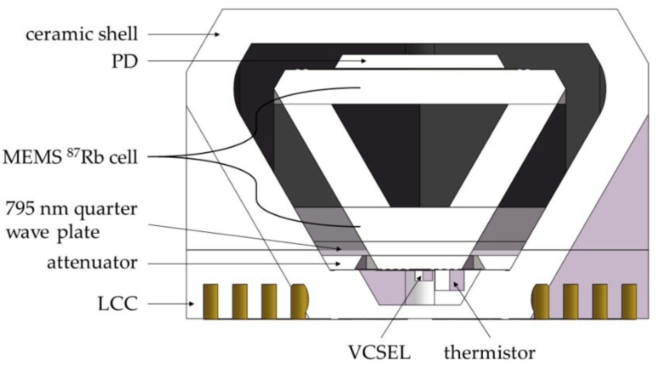
2. Design and Integration of Physics Package

The physics package is the key part of a CSAC, where the coherent population trapping (CPT) signal is produced by the interaction between the circularly polarized 795 nm laser light and the 87Rb atoms, and the CPT signal is interrogated by a PD through the detection of transmission light intensity change. Generally, the components are bonded together by adhesive or epoxy. In order to avoid the deterioration to vacuum by adhesive’s outgassing, we chose eutectic bonding as the integration method. Therefore, adhesive and epoxy were excluded from the physics package. Eutectic bonding is a technique in which an intermediate metal layer creates a eutectic composition with substrates [25]. Table 1 shows the melting point and other properties of different solders used in the physics package [26]. The melting points of solders are restricted to below 410 °C and the melting point difference should be no less than 20 °C. The strength should be large enough. An especially designed physics package is shown in Figure 1 with specially selected materials of low outgassing. The materials will not decompose under the vacuum sealing temperature and work well after vacuum sealing. As shown in Figure 1, the VCSEL is a die with dimensions of 160 × 200 × 150 μm and is bonded to the bottom surface of the attenuator. The VCSEL emits 795 nm linearly polarized laser light. The direction of the linearly polarized laser light is parallel to one edge of the VCSEL pad, as shown by the red solid arrow in Figure 2. In order to sense the temperature of VCSEL precisely, the thermistor is bonded near the VCSEL. A pair of twisted gold wires work as heater to heat the physics package to 85 °C, which satisfies the −40–80 °C temperature range requirement of industrial products. Gold is one of the least reactive chemical elements and the resistance of the heater will keep constant during the physics package assembly. The thermistor, heater and control circuits form a feedback loop controlling the temperature of VCSEL to be stable at 85 °C, which stabilizes the VCSEL output wavelength to the 87Rb D1 line transition. The attenuator is used to reduce the light intensity of laser. Otherwise, the weak CPT signal will be drowned out by the strong background light. The fast axis of the QWP is parallel to one diagonal of the square cross section as illustrated by the purple solid arrow in Figure 2. The angle θ is 45° in such a configuration. Thus, the linearly polarized laser light passes through the QWP, turning into a circularly polarized laser light. The circularly polarized laser light passes into the MEMS 87Rb cell and interacts with 87Rb atoms. The MEMS 87Rb cell is fabricated by anodic bonding silicon with glass at 440 °C, which defines the highest soldering temperature during the physics package integration. The CPT signal is detected by a PD on the top. The leadless chip carriers (LCC) and ceramic shell are vacuum sealed together to keep air from coming into the physics package. The LCC is made from high temperature cofired ceramics (HTCC), which contains more than 91% Al2O3. The ceramic shell consists of more than 95% Al2O3. The ceramic is reported to be second to metals in permeability [27]. However, metals will cause an electrical short when CSACs operate. Low temperature cofired ceramic (LTCC) is also reported to have good hermeticity [28] but it has a worse hermeticity than ceramic. Thus, ceramic is the best choice for hermetic sealing. The components are stacked vertically with each other to minimize the volume. All materials used are compliant with RoHS compliance.
The integration process is shown in Figure 3. In order to minimize the influence of bonding in later steps to bonding in previous steps, the bonding temperature is set to be higher in forward steps. Figure 3a shows the explosive view of part A and the bonding pads on the surfaces of components. The bonding pads are made from gold which will not be oxidized and thus can be bonded without flux in vacuum or inert atmosphere. Before soldering, the gold pads are cleaned by plasma to remove impurities on the surfaces, which will improve the bonding even at a lower temperature. The bonding is performed by eutectic die bonders which have a pulse heat stage (PHS). The PHS provides a preheat temperature before bonding and has the ability to rise from ambient temperature to 400 °C in just 4 s. In addition, the eutectic die bonder is equipped with two N2 nozzles. Namely, the hot N2 nozzle forms the inert atmosphere around the components during the whole bonding process, and the cool N2 nozzle cools the components down after bonding. The hot N2 is used to reduce oxidation during the whole bonding process, which is a prerequisite for flux free eutectic bonding. The integration process of the physics package is divided into four steps. Firstly, the attenuator, QWP, MEMS 87Rb cell and PD are bonded together as Part A by Au88Ge12 solder as illustrated in Figure 3b. The four components are stacked vertically and aligned by the edges. They are put on the PHS and heated to 340 °C for about 15 s. The bonding force is adjusted to about 120 g. A higher preheat temperature, a longer preheat time and a heavier bonding force are required for the multiple surfaces bonding. Then, the temperature of PHS rises to 390 °C for about 10 s. After that, the cool N2 cools Part A down. Secondly, The VCSEL and thermistor are bonded to Part A as Part B by Au80Sn20 as illustrated in Figure 3c. The preheat temperature and time are set to 240 °C and 5 s, respectively. The bonding force is adjusted to be 25 g. Then, the temperature of PHS rises to 300 °C in 5 s and the cool N2 cools the components down. The parameters are all lowered down due to the brittleness and temperature sensitivity of the VCSEL. Thirdly, Part B is bonded to the LCC as Part C by Sn90Sb10, as shown in Figure 3d. The preheat temperature and time are set to be 230 °C and 10 s, respectively. The bonding force is set to be 60 g. The temperature of PHS rises to 270 °C for 10 s and the cool N2 cools Part C down. After that, the bonding pads on the top surface of MEMS cell and PD connect to the LCC by wire bonding. Figure 3e shows an uncompleted physics package which differs from the completed one only in that it is not vacuum sealed. The getter is deposited on the inner surfaces of the ceramic shell. Finally, at the vacuum sealing step, the ceramic shell is bonded to Part C by Sn90Au10 solder. The completed physic package is shown in Figure 3f. The vacuum sealing step is the key to vacuum packaging, which will be discussed in detail in the next section. At the board level, a chip socket is used to connect the physics package to the control circuits for test due to the cleanliness requirement of residual gas analysis. Low melting point solders such as SnBi and SnIn are potential choices.
Thermal dissipation through convection accounts for a large part of power consumption of the physics package [29]. Thus, it is necessary to study the relationship between power consumption of a physics package and vacuum. The uncompleted physics package (as shown in Figure 3e) is put into a vacuum controlled chamber. The power consumption measurement setup is illustrated in Figure 4. The physics package operates at 85 °C. By controlling the pressure in the vacuum chamber, the power consumption of the physics package is measured after the thermistor’s temperature, keeping stable at 85 °C (85 ± 0.01 °C is recognized as stable). The curve of power consumption of three different physics packages under different pressures is illustrated in Figure 5. From Figure 5, we can see that the maximum power consumption is about 135 mW when physics packages are at an atmospheric pressure. When the pressure in vacuum chamber reaches about 1 Pa, the power consumption reaches a minimum of about 10 mW. The curves of different physics packages are similar and monotonic. Thus, the pressure of a physics package with vacuum packaging could be estimated by the power consumption.

3. Vacuum Packaging

The pressure inside a vacuum sealed physics package is the only criteria for vacuum packaging evaluation. However, the inner pressure evolves with time due to many factors. Above all, the vacuum of hermetic sealing furnace determines the highest vacuum inside the physics package. The hermetic sealing furnace used for vacuum packaging here provides a base pressure of 1.33 × 10⁻⁵ Pa. Thus, the main sources of vacuum degradation are the desorption of gas from inner components, the leakage in the sealing and outer covers [30,31]. It is unavoidable to have outgassing due to the thermodynamic interaction between gas and solid [32]. However, the outgassing in a physics package with vacuum packaging could be reduced greatly by prebaking before vacuum sealing. In addition to prebaking, a getter is used to absorb gases from outgassing in a physics package [33,34]. The desorption, leakage detection and getter firing are discussed below.

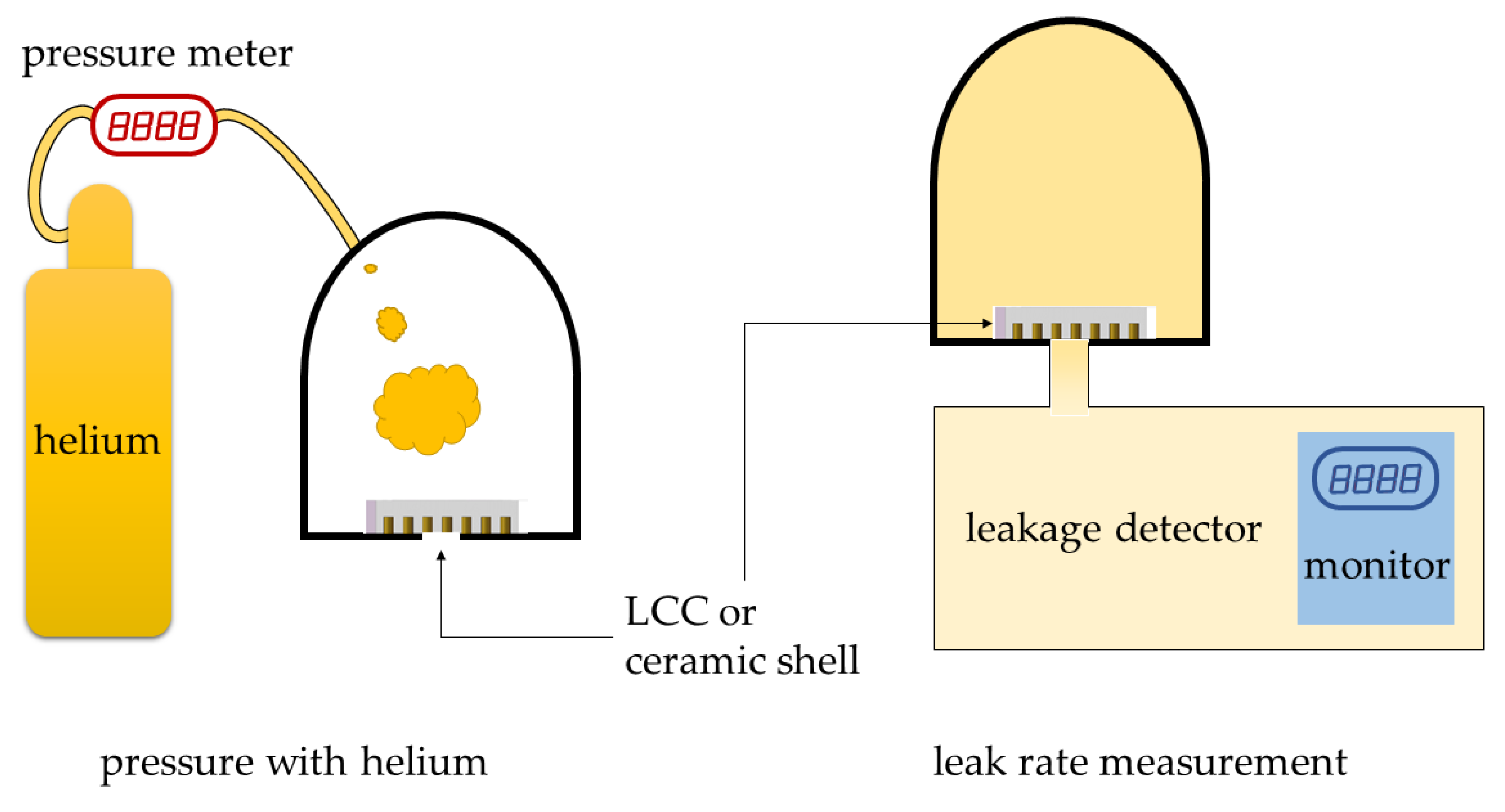
3.1. Hermeticity of LCC and Ceramic Shell

The LCC and ceramic shell keep the air from leaking into the inner space of a completed physics package. Thus, the hermeticity of LCC and ceramic shell should be high enough. Figure 6 shows the schematic diagram of hermeticity measurement of LCC and ceramic shell, which is provided by the supplier. The chamber is pressured with helium first. Then, the leakage detector detects the helium leaked from the LCC or ceramic shell. The leakage of LCC and ceramic shell is measured to be 2.1 × 10⁻¹² Pa·m3/s and 6.4 × 10⁻¹² Pa·m3/s, respectively.

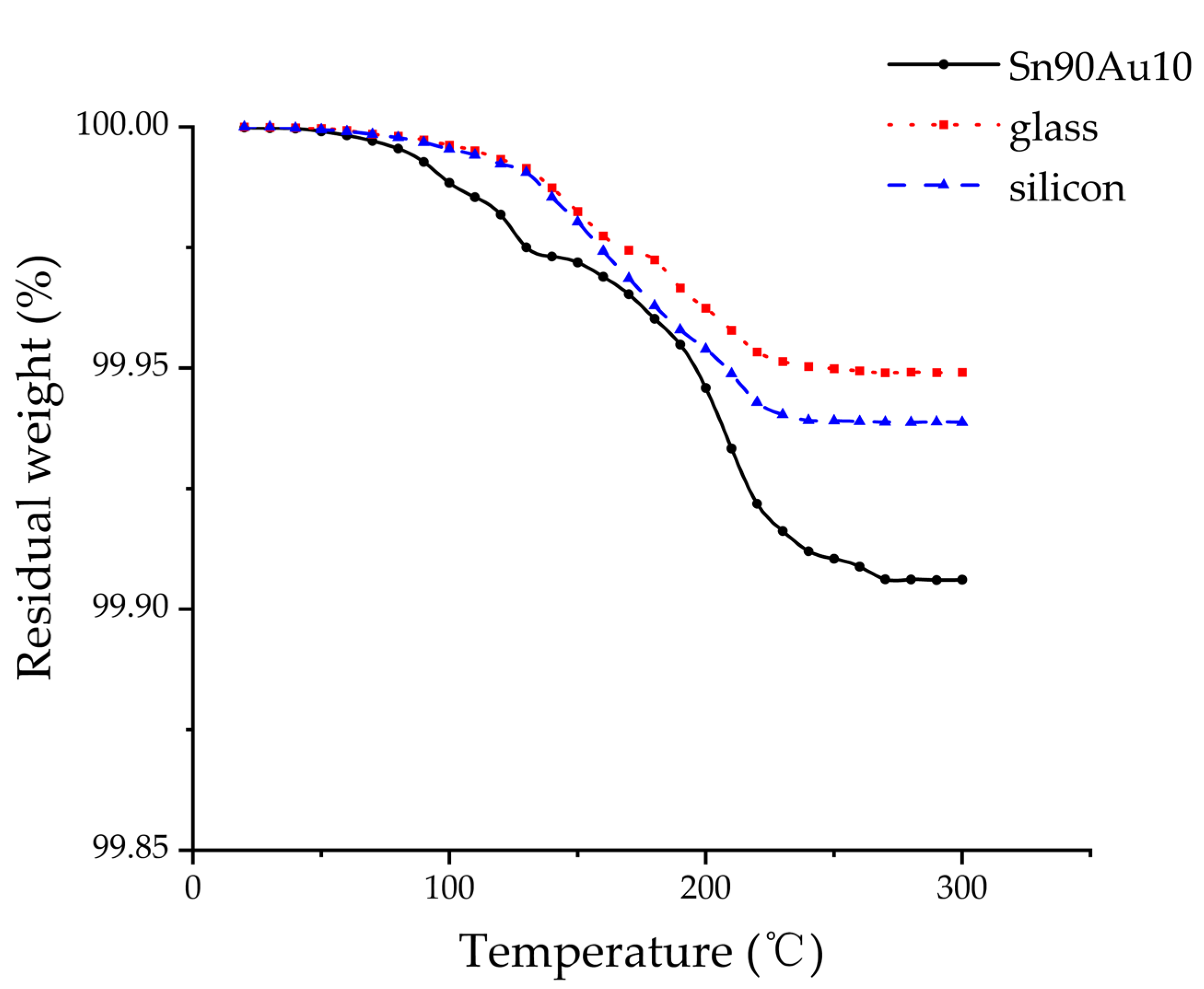
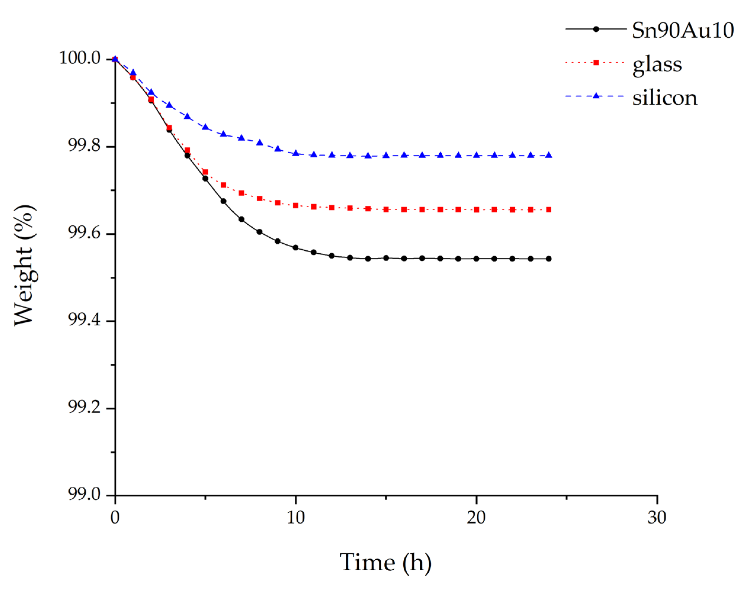
3.2. Outgassing of Materials Used in Physics Package
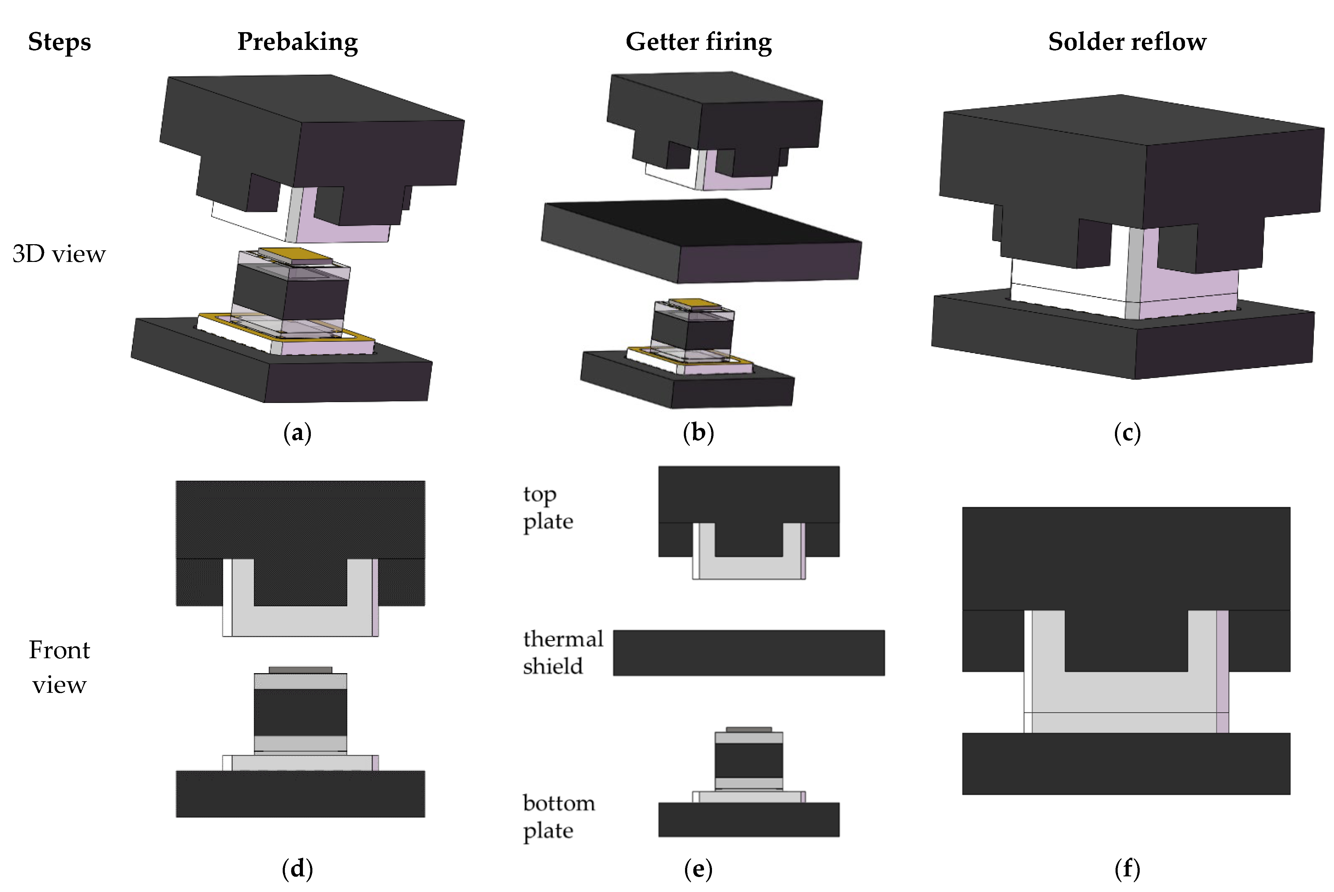
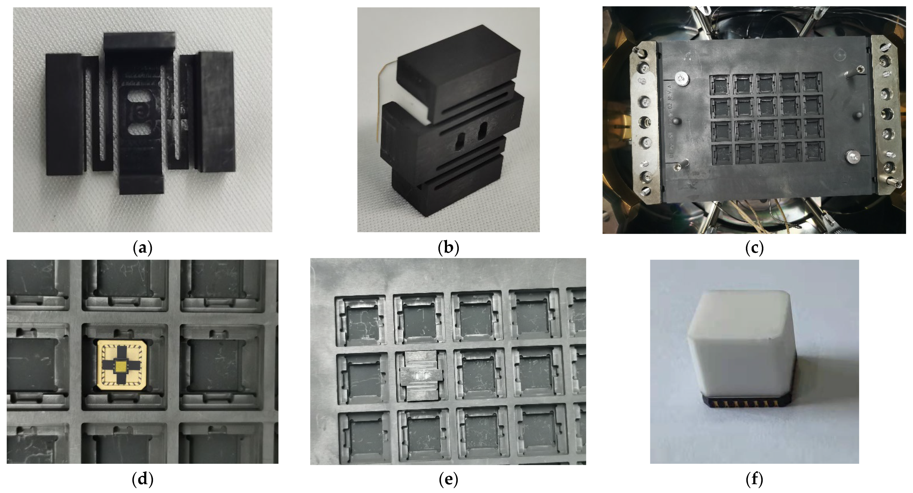
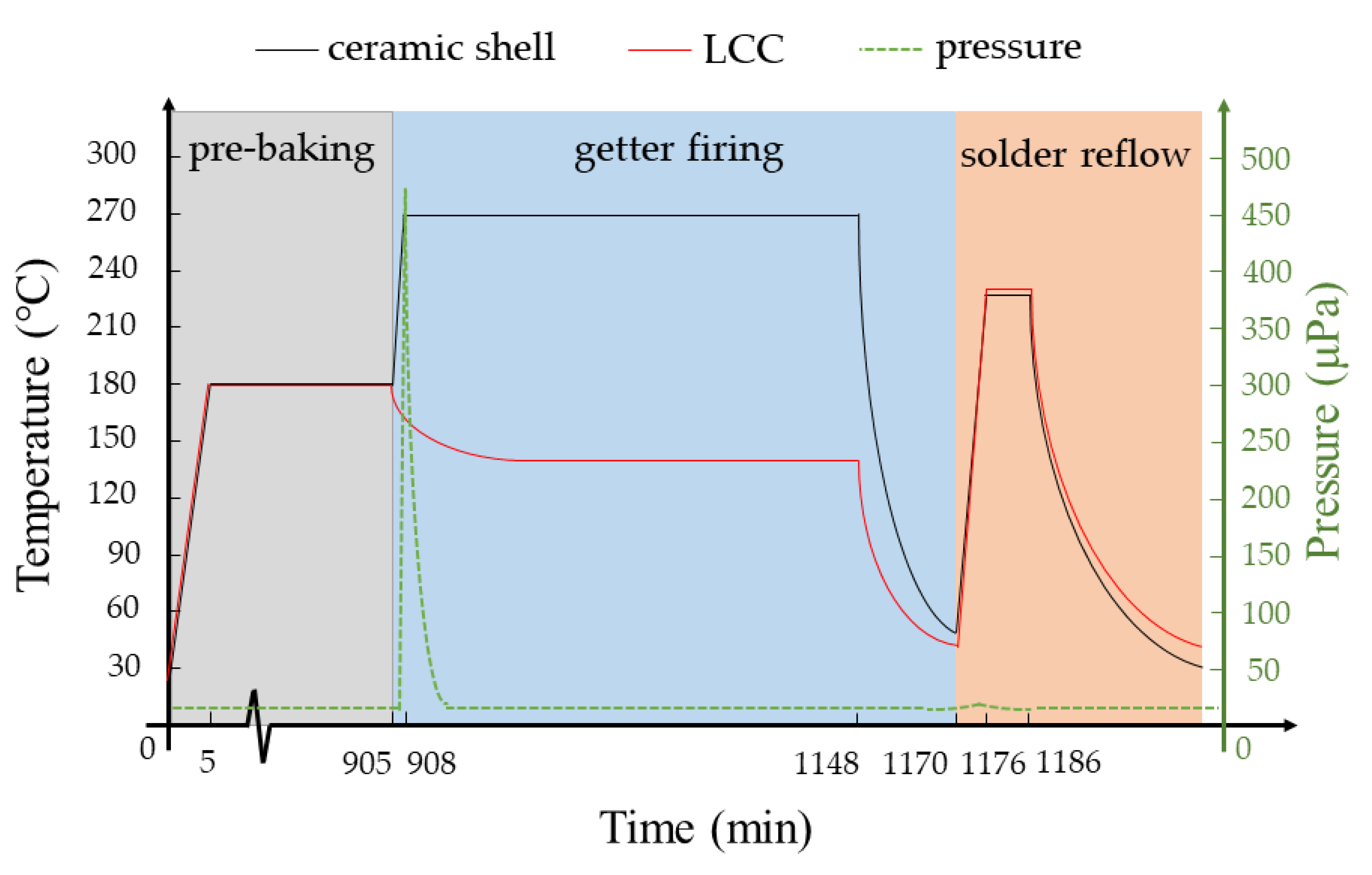
As mentioned above, outgassing of materials is unavoidable. While it is vital to slow the outgassing rate to reduce destruction to the vacuum, the outgassing rate is highly determined by the initial adsorption of gas on the surfaces and in the volume body of components. On the one hand, the surfaces of components are designed to be small and smooth enough to reduce adsorption as much as possible. The use of porous materials is avoided here. On the other hand, an in situ prebaking process is applied to all components before vacuum sealing to enhance the desorption effect.
Temperature and time are the two parameters which should be determined for the prebaking process. The higher the baking temperature and the longer the baking time are, the better the desorption is. However, a very high baking temperature will cause damage to temperature sensitive components such as VCSEL. A very long baking time will increase costs. Therefore, there is a trade-off between the effect of prebaking and baking temperature and time. TGA is widely used to analyze the thermal stability of materials. Typically, TGA is a method in which the mass of a sample is measured over time as the temperature changes [35,36]. In the physics package, the VCSEL includes As, Ga, Al and In. The thermistor is made of many kinds of materials such as platinum, Au and ceramic. However, the VCSEL and thermistor are too small compared to other components and thus the outgassing is neglected. The MEMS 87Rb cell has a good hermeticity and thus its materials are assumed to be silicon and glass. The main material of PD is silicon. The main material of QWP and attenuator is glass. Sn90Au10 has the lowest melting points among the four eutectic solders. Therefore, Sn90Au10, glass and silicon are performed by typical TGA to analyze the thermal stability under vacuum sealing temperature. Besides, the desorption of materials is analyzed through constant temperature TGA. Namely, the mass of materials is measured under a constant temperature for a specific time. Thus, the temperature and time of prebaking are determined from the constant temperature TGA.
At the sample preparation step, all components used in the physics package are cleaned with ultrasonic and baked before crushing into pieces. Then, the pieces are ground into powder. The powder (about 10 mg) is put into the TGA analyzer as a sample for testing.
The typical TGA results of Sn90Au10 solder, glass and silicon are shown in Figure 7. The TGA curves show the weight loss of samples with respect to the temperature increasing from ambient temperature to 300 °C at a rate of 10 °C/min in a nitrogen atmosphere. Even at 300 °C, the maximum weight loss is about 0.1%. Thus, decomposition of materials will not take place at the vacuum sealing temperature of 230 °C, which is much lower than 300 °C.
Similarly, the constant temperature TGA of Sn90Au10 solder, glass and silicon is carried out in a nitrogen atmosphere. The only difference to typical TGA lies in that the mass loss is measured at a constant temperature of 180 °C, which is 37 °C lower than the melting point of Sn90Au10. The constant temperature TGA curves in Figure 8 show that the mass of materials remains unchanging after about 15 h. Namely, the outgassing is almost reduced by baking at 180 °C for 15 h. Thus, the prebaking temperature and time are set to be 180 °C and 15 h in the vacuum, respectively. However, outgassing is almost reduced but will not be eliminated when the mass remains unchanged because the TGA test has a resolution of 0.01 μg and the outgassing will be undiscernible under such a prebaking condition.

3.3. Vacuum Sealing

The vacuum sealing process includes prebaking, in situ getter firing and solder reflow. The getter used in the physics package will be fired at 270 °C for 4 h in accordance with the suggestions from the supplier. However, the melting point of Sn90Au10 is 217 °C. In order to protect components from thermal damage and avoid melting of Sn90Au10 during firing of the getter, the Sn90Au10 solder preform rim is attached to the sealing ring of LCC and the getter is deposited on the inner surface of the ceramic shell, respectively. The Sn90Au10 solder rim is protected by a thermal shield when the getter is firing. Figure 9 shows the configuration of ceramic shell and Part C (defined in Figure 3d) during vacuum sealing. Top plate and bottom plate integrated with thermocouple are two parts of the graphite fixture for accommodating ceramic shell and Part C, respectively. Part C is placed on the bottom plate, while ceramic shell is loaded on the top plate, see Figure 9a. During the prebaking step, Part C and ceramic shell are close and are baked at the same temperature of 180 °C for 15 h to ensure effective desorption, as illustrated in Figure 9a,d. Getter firing follows the prebaking step. Getter requires 270 °C for firing while the Sn90Au10 solder preform rim will be molten under such a high temperature. A thermal shield provided by the vacuum sealing furnace separates the ceramic shell and Part C during getter firing. It affords thermal shielding to Part C and enables firing of getter at 270 °C for 4 h, as illustrated in Figure 9b,e. After that, the thermal shield is removed and the ceramic shell is pushed down to the LCC of Part C. The temperature then reaches the melting point of Sn90Au10 and remains at about 230 °C for a while. The solder rim melts and seals the ceramic shell and LCC together. Figure 9c,f shows the sealing of LCC and ceramic shell in solder reflow step.
The alignment of LCC and ceramic shell during bonding process is performed by the graphite fixture. The graphite fixture consists of the top plate, the middle plate and the bottom plate which are designed for ceramic shell load, components alignment and LCC accommodation, respectively, as shown in Figure 10. The photograph of the top plate is shown in Figure 10a. The Ceramic shell is loaded on the top plate as illustrated in Figure 10b. The bottom plate has a cavity for the LCC accommodation. The middle plate is aligned on to the bottom plate by the fixed rods. The middle plate has the locating hole for alignment of the top plate, as illustrated in Figure 10c. Figure 10d shows that an uncapped physics package (Part C) is accommodated on the bottom plate. Figure 10e shows the alignment of LCC and ceramic shell by placing the top plate into the locating hole of middle plate. Figure 10f shows the physics package after vacuum packaging.
The temperature and pressure profile of vacuum sealing is illustrated in Figure 11. During the whole vacuum sealing process, the pressure in the furnace is controlled to be about 13 μPa, except that a surge of 475 μPa appears when the getter firing starts. The sudden surge in pressure is caused by the accelerated outgassing of getter due to the temperature rising of getter firing. The surge will do no harm to the vacuum of the physics package because it appears far before the solder reflow step. The pressure remains at 13 μPa during the solder reflow step. From the temperature profile of Figure 11, we can see that the temperature of Part C and ceramic shell are at 180 °C during prebaking. When the temperature of the ceramic shell rises to 270 °C during getter firing, the temperature of Part C drops to about 140 °C due to the thermal shield. Thus, the thermal shield protects the Sn90Au10 from melting during getter firing. The temperature of LCC and ceramic shell drops to about room temperature after getter firing. Then, the temperature of LCC and ceramic shell rises to the bonding temperature simultaneously. It is different from the traditional bonding process, where the temperature of the ceramic shell will go down and the temperature of LCC will go up. Their temperatures will meet at the bonding temperature, which will cause a larger thermal gradient in the eutectic solder than the temperature profile shown in Figure 11. A more homogeneous temperature distribution guarantees better wetting and bonding. On the other hand, in the traditional bonding process, the force is generally applied directly to the ceramic shell. As we know, the eutectic solder will melt as long as the temperature is above the liquidus/solidus. The force will cause solder splashing when the eutectic solder changes from solid to liquid suddenly, which may lead to an electrical short in the inner circuits or a poor bonding. Here, the force is applied gradually after the eutectic solder melts, which avoids the solder splashing issue and hence ensures better vacuum packaging.

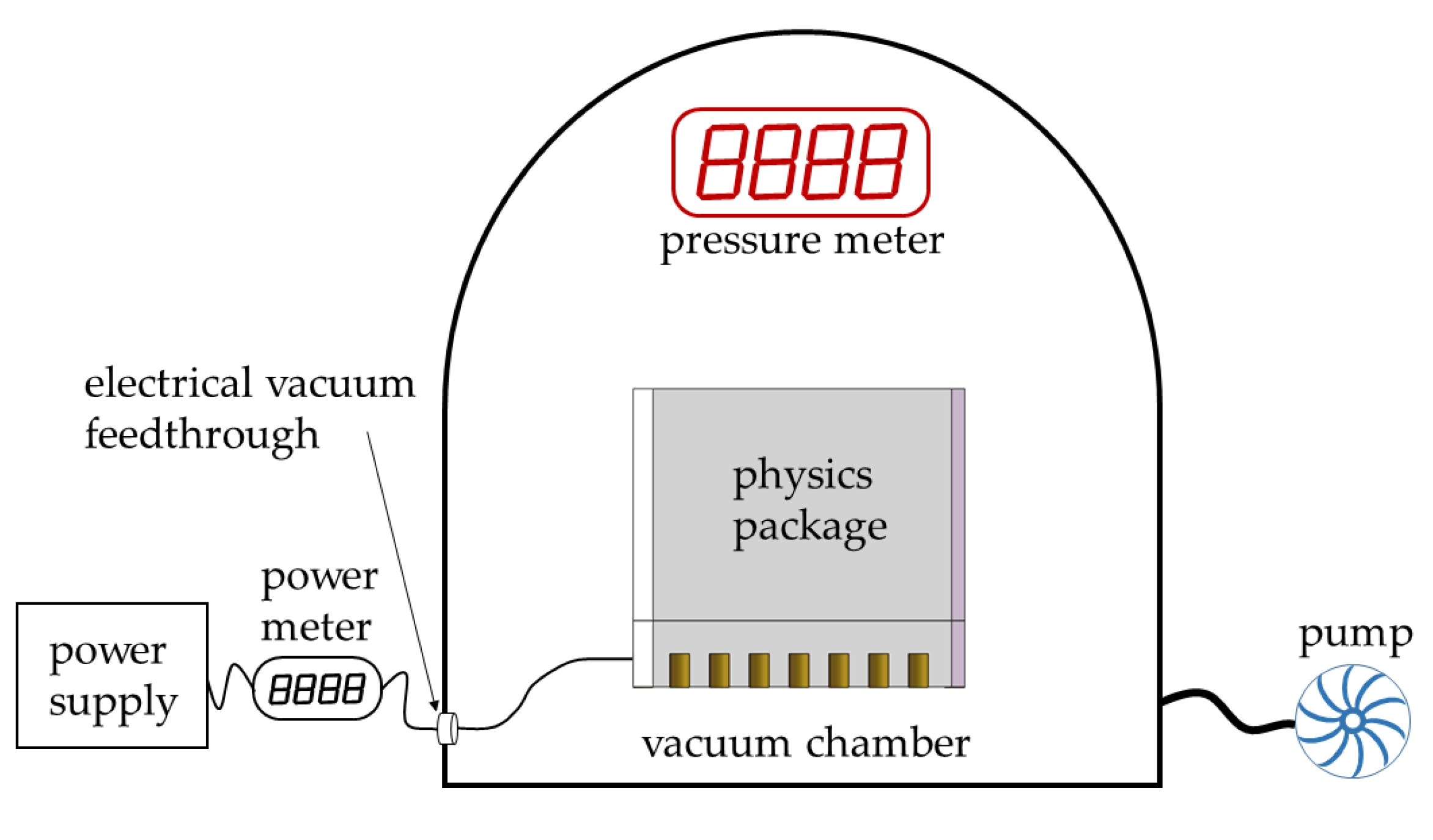
3.4. Leak Rate Test and Residual Gas Analysis
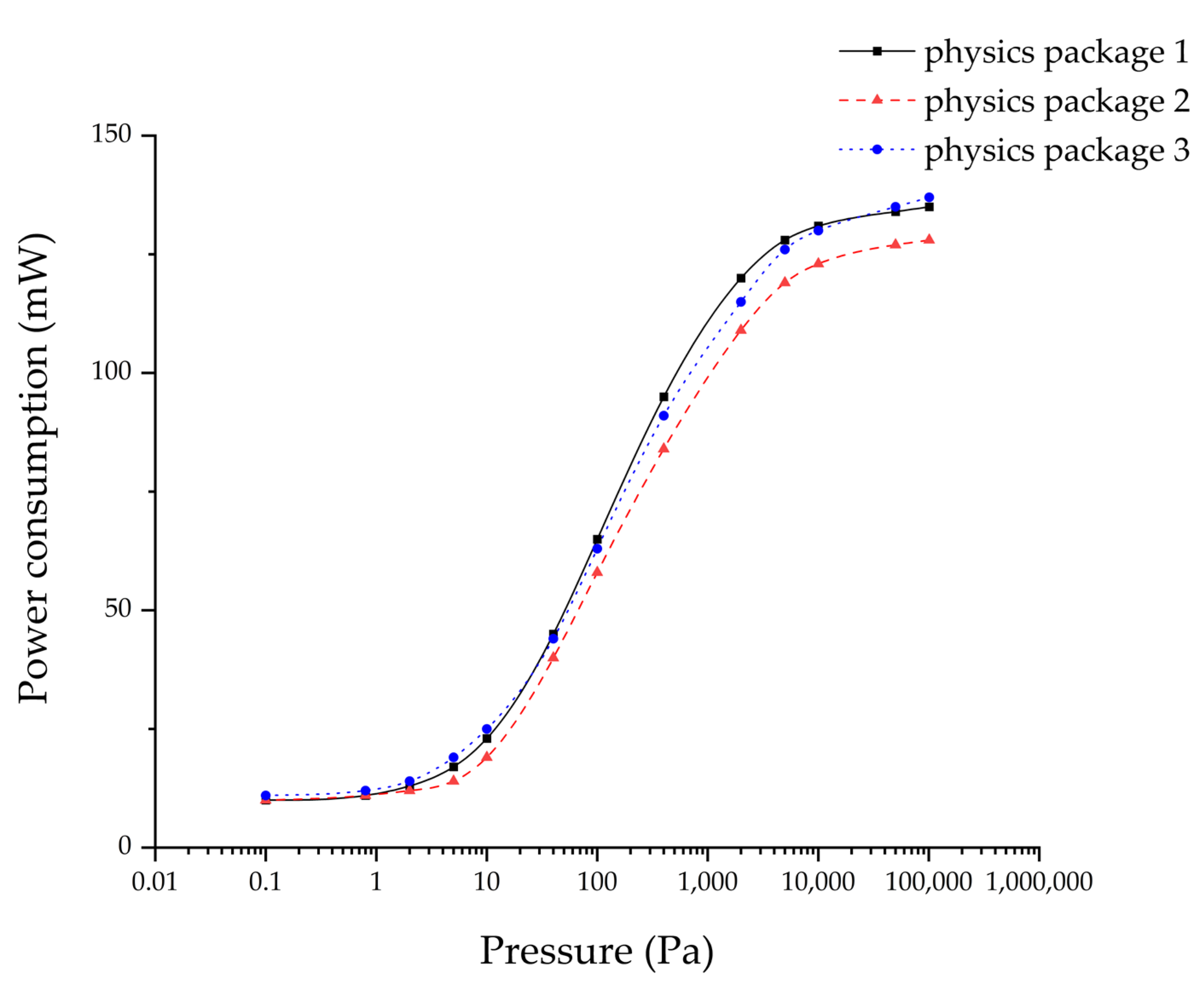
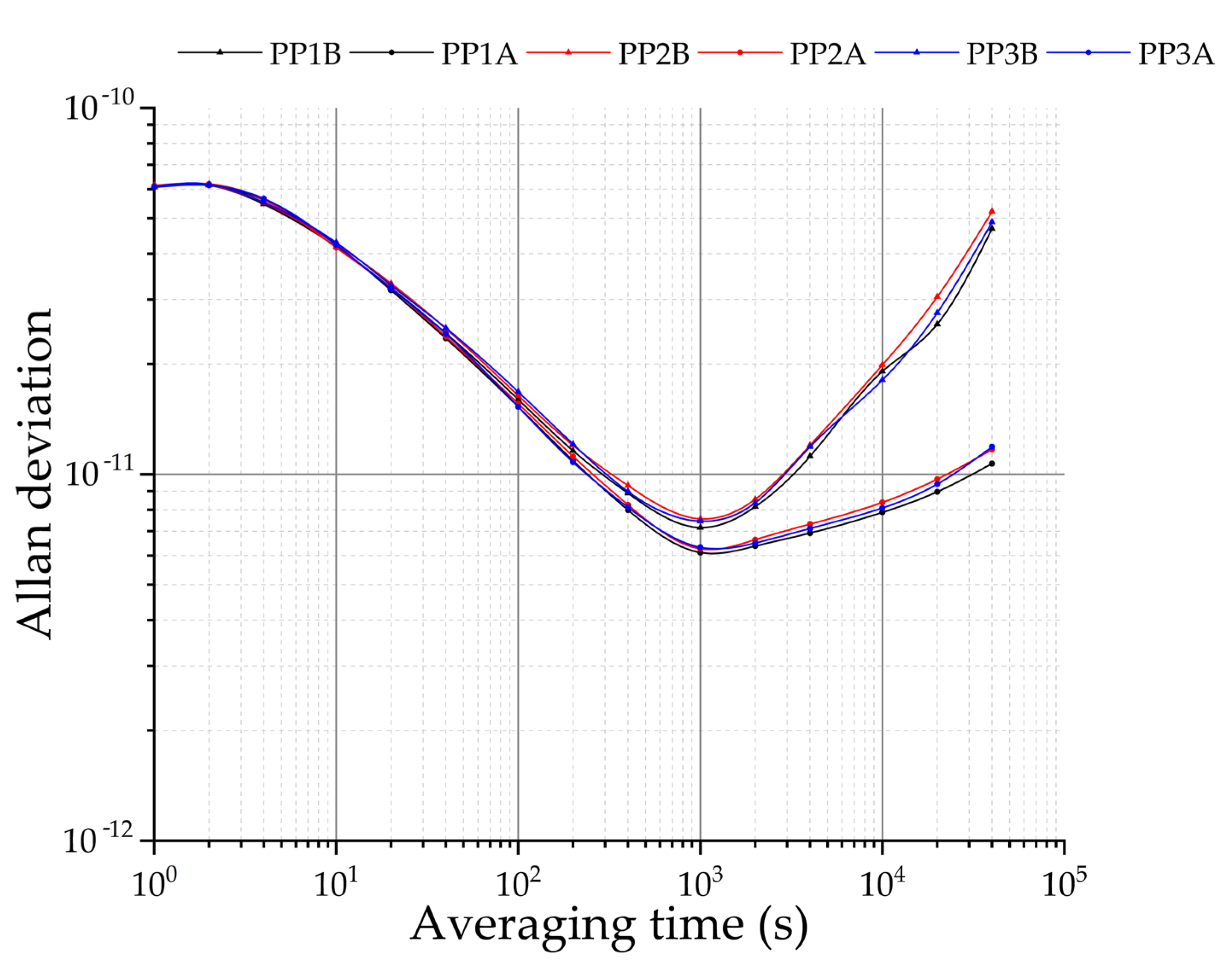
The leak rate of sealing depends on the quality of the eutectic bond between LCC and the ceramic shell. The inspection of sealing and detection of air voids are carried out by X-ray imaging. There are many methods used for the measurement of leak rate in packages containing small cavities, such as helium fine leak, radioisotope fine leak and optical leak [37]. The helium leak rate is measured by helium fine leak as specified in the MIL-STD 883 method 1014 [38] after the X-ray imaging showing defect-free sealing, where the helium bombs at 45 PSIA for a minimum exposure time of 2 h. The result shows that the leak rate is less than 4 × 10⁻¹⁰ Pa m3/s, which is about 10 times better than the maximum leak rate (5 × 10⁻⁹ Pa m3/s) allowable as specified in MIL-883 method 1014 [38]. However, the testing condition of 45 PSIA helium bombing pressure is about three times the atmospheric pressure. Besides, the leakage has an inverse relationship with the relative molecular mass of gases. The relative molecular mass of He is four. Molecules with heavier relative molecular mass such as N2, O2 and CO2 are 28, 32 and 44, which are the main constituents of air. Therefore, the leakage rate of the physics package in air will be much lower than that in the helium bomb condition. In order to get a more precise lifetime of the sealed physics package, the pressure is tested by the residual gas analysis.
Residual gas analysis is widely used in vacuum fields to inspect the change of gases and analyze the composition of gases in MEMS devices [39]. Traditionally, the composition and partial pressure of residual gas are measured by a high sensitive quadrupole mass spectrometer (QMS) gas analyzer [40]. It is helpful to improve the performance of getter from the composition of residual gas. Table 2 shows the results of three different residual gas analyses of physics packages after vacuum packaging. The residual gas analysis is a destructive testing, where the ceramic shell is broken and the gas is analyzed by a QMS. Therefore, three different physics packages are used to test at different time to evaluate the relationship between the inner pressure and time. Physics package 1 is tested 1 month after vacuum sealing. Physics package 2 is tested about 3 months after vacuum sealing. Physics package 3 is tested about 5 months after vacuum sealing. There is no obvious difference in the pressure of the three different physics packages in just several months. From Figure 5, the tolerable vacuum in the physics package is 1 Pa. The power consumption of the physics package at 1 Pa is almost the same with that at 0.1 Pa. The initial pressure in physics package is assumed to be 1.33 × 10⁻⁵ Pa, the same with the background pressure. It takes about 5 months to degrade from 1.33 × 10⁻⁵ Pa to 0.1 Pa. Thus, the time for degradation to 1 Pa is roughly estimated to be about 50 months (~4 years). If the tolerable vacuum is relaxed to 10 Pa, the power consumption of the physics package will increase about a dozen mW. Therefore, the vacuum is allowed to change over 40 years. However, oxidation will occur in the sealing and the hermeticity will be damaged. The actual time for a tolerable vacuum will be shortened.

4. Results

The results of residual gas analysis in Table 2 shows that the inner pressure of physics package is about 0.1 Pa, which is better than the vacuum of 2.7 Pa with adhesives [24]. Nitrogen accounts for most of the residual gas. The leak rate of physics package after vacuum sealing is measured to be less than 4 × 10⁻¹⁰ Pa·m3/s. The power consumption of three different vacuum sealed physics packages is measured to be 13.6, 15.1 and 14.9 mW, respectively, which differs a little from the 10 mW power consumption at 0.1 Pa as illustrated in Figure 5. It is reasonable because there is almost no air in the vacuum chamber when the pressure is 0.1 Pa, as shown in Figure 4. Thus, thermal convection through LCC and ceramic shell to air could be neglected. However, the power consumption of physics package after vacuum packaging is measured in the air. Thermal convection through LCC and ceramic shell to air still exists. This is the basis of the difference.
The frequency performance of the three different physics packages is almost the same, as shown in Figure 12. The short-term stability before and after vacuum packaging is 1.62 × 10⁻¹¹ and 1.52 × 10⁻¹¹ @100 s, respectively, which shows only a little difference. Furthermore, the long-term stability after vacuum packaging is much better than before vacuum packaging. The frequency stability is improved from 4.68 × 10⁻¹¹ to 1.07 × 10⁻¹¹ @40,000 s after vacuum packaging, which is about 4.37 times better. The reason is that temperature change is slow, in the short-term stability range, the impact of temperature change to frequency stability is limited because the ambient temperature may change a little. However, in the long-term stability range, the ambient temperature changes are larger and impact the frequency stability more. The physics package after vacuum packaging has an increased resistance to temperature change, which is beneficial for the frequency stability. The small difference in short term stability also proves that the influence of thermal stress to the physics package during vacuum sealing could be neglected. Compared to SA.45s which has a frequency performance of 3 × 10⁻¹¹ @100 s and 1 × 10⁻¹¹ @1000 s [41], the frequency performance of the proposed physics package is better.

5. Discussion

A systematic high vacuum packaging method for MEMS devices is proposed and introduced thoroughly in this paper, from low outgassing materials selection, prebaking, getter firing and solder reflow to inspection technologies after vacuum packaging including X-ray imaging, leak rate test and residual gas analysis. The results show that a high vacuum (about 0.1 Pa) is achieved, which is mainly caused by the ongoing desorption after vacuum packaging. The method is of high reference value for other researchers to perform vacuum packaging to their MEMS devices. Although the specific conditions are different from various kinds of MEMS devices, the method provides a general guideline for high vacuum packaging. Anyone could customize their own vacuum packaging parameters by adopting this method.
The problem is easily located when using the method properly even if one fails to obtain the high vacuum. A high leak rate may be caused by a defect bonding and the X-ray imaging will verify this. The TGA of materials will reveal the outgassing and thermal stability under vacuum sealing. Besides, the recipe of getter could be adjusted according to the gas composition of residual gas analysis. For some applications where a lower vacuum is required, such as MEMS gyroscopes (the inner pressure is about 70 Pa) with wide bandwidth and wide linear input range [42], adhesive bonding could be used to integrate components for convenience. Adhesive bonding has the advantage of insensitivity to surface topography and the ability to join different types of materials [43]. However, the higher outgassing of adhesive will do much more harm to vacuum than eutectic solders. For other applications where a higher vacuum is required, the getter should be activated at a higher temperature to increase the gas absorption rate. The components are better to be baked at a higher temperature for a longer time to eliminate the desorption as much as possible, as long as the components have the ability to withstand a harsher baking condition. In conclusion, the method proposed is a systematic way for MEMS devices to obtain a high vacuum.

Author Contributions

Conceptualization, P.G. and J.Z.; methodology, P.G. and H.M.; software, P.G. and L.D.; validation, P.G., H.M. and L.D.; formal analysis, P.G. and H.X.; investigation, P.G.; resources, H.M. and J.Z.; data curation, P.G., L.D. and J.Z.; writing—original draft preparation, P.G.; writing—review and editing, L.D., H.X. and J.Z.; visualization, H.M.; supervision, J.Z.; project administration, J.Z.; funding acquisition, H.M. and J.Z. All authors have read and agreed to the published version of the manuscript.

Funding

This work was funded by the National Natural Science Foundation of China, Grant No. 91836301 & No. 61535001.

Institutional Review Board Statement

Not applicable.

Informed Consent Statement

Not applicable.

Data Availability Statement

Data are contained within the article.

Acknowledgments

Thanks to the Zhongkeqidi Optoelectronic Technology (Guangzhou) Co., Ltd. for providing us with the vacuum sealing furnace and other equipment for experiment.

Conflicts of Interest

The authors declare no conflict of interest.

References

  1. Lee, S.H.; Mitchell, J.; Welch, W.; Lee, S.; Najafi, K. Wafer-level vacuum/hermetic packaging technologies for MEMS. In Reliability, Packaging, Testing, and Characterization of MEMS/MOEMS and Nanodevices IX; SPIE: San Francisco, CA, USA, 2010; Volume 7592, p. 759205. [Google Scholar] [CrossRef]
  2. Moelders, N.; Daly, J.T.; Greenwald, A.C.; Johnson, E.A.; McNeal, M.P. Localized, in-situ vacuum measurements for MEMS packaging. Mat. Res. Soc. Symp. Proc. 2003, 782. [Google Scholar] [CrossRef]
  3. Knowles, K.M.; Van Helvoort, A.T. Anodic bonding. Int. Mater. Rev. 2006, 51, 273–311. [Google Scholar] [CrossRef]
  4. Henmi, H.; Shoji, S.; Shoji, Y.; Yoshimi, K.; Esashi, M. Vacuum packaging for microsensors by glass-silicon anodic bonding. Sens. Actuators A 1994, 43, 243–248. [Google Scholar] [CrossRef]
  5. Knapkiewicz, P. Technological assessment of MEMS alkali vapor cells for atomic references. Micromachines 2019, 10, 25. [Google Scholar] [CrossRef] [Green Version]
  6. Wang, Q.; Choa, S.H.; Kim, W.; Hwang, J.; Ham, S.; Moon, C. Application of Au-Sn eutectic bonding in hermetic radio-frequency microelectromechanical system wafer level packaging. J. Elec. Materi. 2006, 35, 425–432. [Google Scholar] [CrossRef]
  7. Knechtel, R.; Wiemer, M.; Frömel, J. Wafer level encapsulation of microsystems using glass frit bonding. Microsyst. Technol. 2006, 12, 468–472. [Google Scholar] [CrossRef]
  8. Sparks, D.; Massoud-Ansari, S.; Najafi, N. Long-term evaluation of hermetically glass frit sealed silicon to Pyrex wafers with feedthroughs. J. Micromech. Microeng. 2005, 15, 1560. [Google Scholar] [CrossRef]
  9. Walsh, C.A. Laser Welding-Literature Review; University of Cambridge: Cambridge, UK, 2002. [Google Scholar]
  10. Di Cioccio, L.; Gueguen, P.; Taibi, R.; Landru, D.; Gaudin, G.; Chappaz, C.; Rieutord, F.; de Crecy, F.; Radu, I.; Chapelon, L.L.; et al. An overview of patterned metal/dielectric surface bonding: Mechanism, alignment and characterization. J. Electrochem. Soc. 2011, 158, 81. [Google Scholar] [CrossRef] [Green Version]
  11. Lee, S. Fundamentals of thermal compression bonding technology and process materials for 2.5/3D packages. In 3D Microelectronic Packaging; Springer: Cham, Switzerland, 2017; pp. 157–203. [Google Scholar] [CrossRef]
  12. Den Besten, C.; Van Hal, R.E.; Munoz, J.; Bergveld, P. Polymer bonding of micro-machined silicon structures. In Proceedings of the IEEE Micro Electro Mechanical Systems, Travemünde, Germany, 4–7 February 1992; pp. 104–109. [Google Scholar] [CrossRef] [Green Version]
  13. Borzenko, T.; Tormen, M.; Schmidt, G.; Molenkamp, L.W.; Janssen, H. Polymer bonding process for nanolithography. Appl. Phys. Lett. 2001, 79, 2246–2248. [Google Scholar] [CrossRef]
  14. Jiang, M.; Tao, W.; Chen, Y. Laser welding under vacuum: A review. Appl. Sci. 2017, 7, 909. [Google Scholar] [CrossRef] [Green Version]
  15. Qin, Y.; Howlader, M.M.; Deen, M.J.; Haddara, Y.M.; Selvaganapathy, P.R. Polymer integration for packaging of implantable sensors. Sens. Actuators B 2014, 202, 758–778. [Google Scholar] [CrossRef]
  16. Higurashi, E.; Suga, T. Review of low-temperature bonding technologies and their application in optoelectronic devices. Electron. Comm. Jpn. 2016, 99, 63–71. [Google Scholar] [CrossRef]
  17. Knechtel, R. Glass frit bonding: An universal technology for wafer level encapsulation and packaging. Microsyst. Technol. 2005, 12, 63–68. [Google Scholar] [CrossRef]
  18. Shimatsu, T.; Uomoto, M. Room temperature bonding of wafers with thin nanocrystalline metal films. ECS Trans. 2010, 33, 61. [Google Scholar] [CrossRef]
  19. Xie, J.; Lu, S.; Du, Y.; Hu, W.; Mao, Y. Microstructural evolution and orientation-correlated origin of the coarsening behaviors in Au–Sn eutectic alloys. J. Alloys Compd. 2019, 806, 1285–1291. [Google Scholar] [CrossRef]
  20. Peng, J.; Liu, H.S.; Ma, H.B.; Shi, X.M.; Wang, R.C. Microstructure evolution and mechanical reliability of Cu/Au–Sn/Cu joints during transient liquid phase bonding. J. Mater. Sci. 2018, 53, 9287–9296. [Google Scholar] [CrossRef]
  21. Liu, S.; Zhang, D.; Xiong, J.; Chen, C.; Song, T.; Liu, L.; Huang, S. Microstructure evolution and properties of rapidly solidified Au-20Sn eutectic solder prepared by single-roll technology. J. Alloys Compd. 2019, 781, 873–882. [Google Scholar] [CrossRef]
  22. Wen, L.; Xue, S.; Wang, L.; Liu, H.; Wu, J. Microstructural evolution and shear performance of AuSn20 solder joint under gamma-ray irradiation and thermal cycling. J. Mater. Sci. Mater. Electron. 2020, 31, 7200–7210. [Google Scholar] [CrossRef]
  23. Kuhmann, J.F.; Preuss, A.; Adolphi, B.; Maly, K.; Wirth, T.; Oesterle, W.; Pittroff, W.; Weyer, G.; Fanciulli, M. Oxidation and reduction of eutectic SnPb, InSn, and AuSn: A knowledge base for fluxless solder bonding applications. IEEE Trans. Compon. Pack. Manuf. Tech. 1998, 21, 134–141. [Google Scholar] [CrossRef]
  24. Tepolt, G.B.; Mescher, M.J.; LeBlanc, J.J.; Lutwak, R.; Vargheses, M. Hermetic vacuum sealing of MEMS devices containing organic components. In SPIE Reliability, Packaging, Testing, and Characterization of MEMS/MOEMS and Nanodevices IX; SPIE: San Francisco, CA, USA, 2010; Volume 7592. [Google Scholar] [CrossRef]
  25. Prakash, S.; Yeom, J. Advanced fabrication methods and techniques. In Nanofluidics and Microfluidics: Systems and Applications, 1st ed.; William Andrew: Waltham, MA, USA, 2014; pp. 87–170. [Google Scholar]
  26. MatWeb. Available online: http://matweb.com (accessed on 21 July 2021).
  27. Jiang, G.; Zhou, D.D. Technology advances and challenges in hermetic packaging for implantable medical devices. In Implantable Neutral Prostheses, 2nd ed.; Springer: New York, NY, USA, 2009; pp. 27–61. [Google Scholar]
  28. Goeke, R.S.; Grubbs, R.K.; Yazzie, D.; Casias, A.L.; Peterson, K.A. Gas permeation measurements on low temperature cofired ceramics. Addit. Conf. Device Packag. HiTEC HiTEN CICMT 2012, 2012, 3232–3327. [Google Scholar] [CrossRef]
  29. Kitching, J.; Knappe, S.; Schwindt, P.D.; Shah, V.; Hollberg, L.; Liew, L.A.; Moreland, J. Power dissipation in a vertically integrated chip-scale atomic clock. In Proceedings of the 2004 IEEE International Frequency Control Symposium and Exposition, Montreal, QC, Canada, 23–27 August 2004; pp. 781–784. [Google Scholar] [CrossRef]
  30. Marinis, T.F.; Soucy, J.W. Vacuum packaging of MEMS inertial sensors. In Proceedings-SPIE the International Society for Optical Engineering; SPIE: Boston, MA, USA, 2003; pp. 386–391. [Google Scholar]
  31. Choa, S.H. Reliability of MEMS packaging: Vacuum maintenance and packaging induce stress. Microsyst. Technol. 2005, 11, 1187–1196. [Google Scholar] [CrossRef]
  32. Rizzi, E.; Mauri, L.; Moraja, M.; Conte, A.; Bonucci, A.; Longoni, G.; Amiotti, M. Outgassing and gettering. In Handbook of Silicon Based MEMS Materials and Technologies, 2nd ed.; Tilli, M., Mottoka, M., Airaksinen, V.M., Franssila, S., Paulasto-Krockel, M., Lindroos, V., Eds.; Elsevier: New York, NY, USA, 2015; pp. 713–733. [Google Scholar] [CrossRef]
  33. Benvenuti, C.; Chiggiato, P.; Pinto, P.C.; Santana, A.E.; Hedley, T.; Mongelluzzo, A.; Ruzinov, V.; Wevers, I. Vacuum properties of TiZrV non-evaporable getter films. Vacuum 2001, 60, 57–65. [Google Scholar] [CrossRef] [Green Version]
  34. Benvenuti, C.; Chiggiato, P.; Cicoira, F.; Ruzinov, V. Decreasing surface outgassing by thin film getter coatings. Vacuum 1998, 50, 57–63. [Google Scholar] [CrossRef]
  35. Coats, A.W.; Redfern, J.P. Thermogravimetric Analysis: A review. Analyst 1963, 88, 906–924. [Google Scholar] [CrossRef]
  36. Prime, R.B.; Bair, H.E.; Vyazovkin, S.; Gallagher, P.K.; Riga, A. Thermogravimetric analysis (TGA). In Thermal Analysis of Polymers: Fundamentals and Applications, 1st ed.; Menczel, J.D., Prime, R.B., Eds.; John Wiley & Sons, Inc.: Hoboken, NJ, USA, 2009; pp. 319–386. [Google Scholar]
  37. Costello, S.; Desmulliez, M.P.; McCracken, S. Review of test methods used for the measurement of hermeticity in packages containing small cavities. IEEE Trans. Compon. Pack. Manuf. Technol. 2021, 2, 430–438. [Google Scholar] [CrossRef] [Green Version]
  38. EverySpec. Available online: http://everyspec.com (accessed on 7 September 2021).
  39. Anufriev, G.S.; Boltenkov, B.S.; Ryabinkov, A.I. High-resolution mass spectra of the residual gas in a metallic vacuum system. Tech. Phys. 2006, 51, 100–111. [Google Scholar] [CrossRef]
  40. Lichtman, D. Residual gas analysis: Past, present, and future. J. Vac. Sci. Technol. A 1990, 8, 2810–2813. [Google Scholar] [CrossRef]
  41. Microchip (Microsemi Product Porfolio). Available online: http://microsemi.com (accessed on 8 September 2021).
  42. Prikhodko, I.P.; Simon, B.R.; Sharma, G.; Zotov, S.A.; Trusov, A.A.; Shkel, A.M. High and moderate-level vacuum packaging of vibratory MEMS. In Proceedings of the 46th International Symposium on Microelectronics, Orlando, FL, USA, 30 September–3 October 2013; pp. 705–710. [Google Scholar]
  43. Niklaus, F.; Stemme, G.; Lu, J.Q.; Gutmann, R.J. Adhesive wafer bonding. J. Appl. Phys. 2006, 99, 2. [Google Scholar] [CrossRef]
Figure 1. Design of the physics package.
Applsci 11 08536 g001
Figure 2. The bottom view of the attenuator.
Applsci 11 08536 g002
Figure 3. Integration process of the physics package: (a) explosive view of Part A; (b) integration of Part A; (c) integration of Part B; (d) integration of Part C; (e) an uncompleted physics package; (f) a completed physics package.
Applsci 11 08536 g003
Figure 4. The measurement setup of power consumption under different pressure.
Applsci 11 08536 g004
Figure 5. Electric power consumption of physics packages depending on cavity gas pressure when the VCSEL is ovenized to 85 °C.
Applsci 11 08536 g005
Figure 6. The schematic diagram shows the hermeticity measurement of LCC and ceramic shell.
Applsci 11 08536 g006
Figure 7. Typical TGA results of Sn90Au10 solder, glass and silicon.
Applsci 11 08536 g007
Figure 8. Constant temperature TGA at 180 °C of Sn90Au10 solder, glass and silicon.
Applsci 11 08536 g008
Figure 9. The configuration of ceramic shell and LCC during vacuum sealing. (a) the 3D view of Part C accommodated by bottom plate and ceramic shell loaded on the top plate during prebaking; (b) the 3D view of ceramic shell and Part C are separated by a thermal shield during getter firing; (c) the 3D view of ceramic shell is pushed down to the LCC of part C during solder reflow; (d) the front view of LCC accommodated by bottom plate and ceramic shell loaded on the top plate during prebaking; (e) the front view of configuration of ceramic shell and Part C during getter firing; (f) the front view of configuration of ceramic shell and Part C during solder reflow.
Applsci 11 08536 g009
Figure 10. Photographs show the alignment configuration during vacuum packaging. (a) The photograph of the top plate; (b) the photograph shows that the ceramic shell is loaded on the top plate; (c) the photograph shows the middle plate on the bottom plate; (d) the photograph shows that Part C is accommodated on the bottom plate; (e) the photograph shows the configuration of graphite fixture after alignment; (f) the photograph shows a physics package after vacuum packaging.
Applsci 11 08536 g010
Figure 11. Temperature and pressure profile during vacuum sealing.
Applsci 11 08536 g011
Figure 12. Frequency stability of the 3 different physics packages before and after vacuum packaging. PP1B: physics package 1 before vacuum packaging; PP1A: physics package 1 after vacuum packaging; PP2B: physics package 2 before vacuum packaging; PP2A: physics package 2 after vacuum packaging; PP3B: physics package 3 before vacuum packaging; PP3A: physics package 3 after vacuum packaging.
Applsci 11 08536 g012
Table 1. Properties of different eutectic solders.
Solder AlloyIngredients (Weight %)Melting Point (°C)Shear Strength (MPa)Tensile Strength (MPa)
Sn90Au10Sn/Au = 90/102175050
Sn90Sb10Sn/Sb = 90/102504444
Au80Sn20Au/Sn = 80/20280275.8275.8
Au88Ge12Au/Ge = 88/12356185185
Table 2. Residual gas analysis results of 3 different physics packages after vacuum packaging tested at different time.
Sample IDPhysics Package 1Physics Package 2Physics Package 3
Test time after vacuum packagingmonths135
Power consumptionmW13.615.114.9
PressurePa0.0930.1040.098
Nitrogen%99.799.299.4
OxygenppmNDNDND
Argonppm<100164105
Carbon dioxideppm136439731639
Moistureppm247321841367
Hydrogenppm482853717
Ammoniappm583379942
Fluorocarbonsppm164128154
Publisher’s Note: MDPI stays neutral with regard to jurisdictional claims in published maps and institutional affiliations.

