Abstract
The graphene-based Field Effect Transistors (GFETs), due to their multi-parameter characteristics, are growing rapidly as an important detection component for the apt detection of disease biomarkers, such as DNA, in clinical diagnostics and biomedical research laboratories. In this paper, the non-equilibrium Green function (NEGF) is used to create a compact model of GFET in the ballistic regime as an important building block for DNA detection sensors. In the proposed method, the self-consistent solutions of two-dimensional Poisson’s equation and NEGF, using the nearest neighbor tight-binding approach on honeycomb lattice structure of graphene, are modeled as an efficient numerical method. Then, the eight parameters of the phenomenological ambipolar virtual source (AVS) circuit model are calibrated by a least-square curve-fitting routine optimization algorithm with NEGF transfer function data. At last, some parameters of AVS that are affected by induced charge and potential of DNA biomolecules are optimized by an experimental dataset. The new compact model response, with an acceptable computational complexity, shows a good agreement with experimental data in reaction with DNA and can effectively be used in the plan and investigation of GFET biosensors.
1. Introduction
The early diagnosis of diseases such as viral infections and cancer cell disorders is crucial and significantly improves patient survival. In recent years, Different detection strategies are categorized into amplification techniques such as RT-PCR, Reverse Transcription Polymerase Chain Reaction, detection based on biosensors, and immunological assays such as ELIZA (Enzyme-Linked Immunosorbent Assay). The amplification-based techniques need complex and expensive instruments and expert personnel and a longer time for completion, whereas immunological assays require a complex production process to recombinant biological molecules and antibodies [1]. However, both methods are time-consuming and need costly and complex optical imaging instruments. Thus, researchers are searching for a reliable, low-cost, and easy way for the selective detection of disease biomarkers with sufficient precision. In recent methods for the detection of disease biomarkers such as DNA, biosensing is the most efficient procedure. The biosensors are composed of five parts, a bio-receptor (e.g., enzyme, antibody, aptamer, DNA), a physiochemical transducer (e.g., electrochemical, optical, pyroelectric, FET-based, piezoelectric), an amplifier, a processor, and a display. GFET-based biosensors provide significant advantages over other mentioned methods due to the new sensing and high sensitivity mechanisms, ease and cost-effectiveness of wafer fabrication, and label-free and rapid detection in a non-destructive form [2]. Different types of FET-based biosensors are ion-sensitive field-effect transistors (ISFET), biologically sensitive FET (BioFET), DNAFET, and GFET. Due to a zero band structure and high electrical conductivity of graphene, different types of graphene devices such as single-layer nanoribbons (GNRs) and multilayer graphene nanoribbons (MLGNRs), graphene oxide, multilayer graphene (MLG), and carbon nanotubes (CNT) are exceptionally promising materials as a channel of FET for nanoelectronic biosensors [3,4]. Recent advances in GFET-based biosensors have improved the detection and diagnosis of different diseases such as SARS-CoV-2 (COVID-19), bacteria infections, cancer cell disorders, and so on. Unfortunately, the accurate design of GFET-based biosensors needs nanoscale experimental equipment despite its high price. This shortcoming creates a challenge to overcome this deficiency in the design of the GFET biosensor by modeling it and testing new materials and different structures to improve biosensor parameters such as the limit of detection, LOD, dynamic range, selectivity, and sensitivity. Although excellent efforts have been accomplished experimentally, the modeling of the GFET operation is essential to advance development and optimization for different applications. There are only a few reports on the modeling and simulation of GFET-based biosensors. Within the previously proposed models, the surface graphene response with DNA molecules has been modeled by the carrier mobility, transfer characteristics, surface capacitance, and conductivity of graphene [5,6,7,8,9,10,11,12,13]. In [5], doping effects of graphene surface functionalization were investigated. In the proposed method, the PBASE (1-pyrenebutanoic acid succinimidyl ester) was immobilized on a graphene surface, and two solvents, dimethyl formamide (DMF) and methanol (CH3OH), were used to dissolve PBASE. Raman spectra analysis and electrical measurement revealed that PBASE imposes a p-doping effect while DMF and CH3OH impose an n-doping effect. In [6], the incremental Support Vector Regression, ISVR, algorithm was used to detect interferon-gamma by the aptamer-functionalized GFETs, that the shift of neutral point voltage was mathematically modeled and simulated. In the proposed model, a GFET-based biosensor was employed for tuberculosis susceptibility detection by its interferon-gamma biomarker. In the proposed method, the graphene surface carrier concentration and drain-source current would change when the interferon-gamma molecules attach to the surface of graphene. To create a pattern for drain-source current, an ISVR algorithm was employed that shows an acceptable agreement between outcomes of ISVR and experimental data. Recently, the modeling of GFETs for the detection of DNA hybridization has been employed [7,8]. In [7], a quantum capacitance-sensitive model for a GFET was established, which shows more than 97% accuracy. In the proposed method, a theoretical parametric model for quantum capacitance has been constructed; then, the unknown parameters are estimated by an ant-colony optimization (ACO) algorithm to decrease error with experimental data.
In [8], the source-drain current versus gate-source voltage was modeled by a parabolic parametric function of DNA concentration with three parameters. In the proposed method, three parameters are estimated via experimental data by particle swarm optimization (PSO), where the graphene channel of FET was functionalized by single-stranded DNA and was exposed to the complementary DNA. In [9], an efficient numerical approach was proposed for modeling of transport of armchair graphene ribbon. This method is based on an envelope function in the reciprocal space and a recursive matrix approach that the computation time was decreased with respect to the finite difference method.
Additionally, references [10] and [11] for Escherichia coli detection employed G-FETs and functionalized it by antibody and aptamer sensing probes, respectively. In the proposed method, GFETs were experimentally modified with PBASE 1-pyrenebutanoic acid succinimidyl ester and E. coli antibodies [10] pyrene-tagged aptamer [11]. The results show the electrical response depends on Escherichia coli concentration. In [12], a liquid-gated GFET based biosensor model is analytically developed for Escherichia Coli O157:H7 bacteria detection by simulation of its effects on the graphene surface in the form of conductance variation. Additionally, the GFET current-voltage characteristics as a function of E. coli concentration were modeled. In [13], a computational approach was proposed to build state-space models (SSMs) for the time-series data of a G-FET biosensor. The SSMS model parameters were estimated through Markov chain Monte Carlo methods. The Bayesian information criterion evaluation of SSMs showed that SSMs well fitted the time-series data of the G-FET biosensor. Although these models can be used in special situations, they suffer from accuracy due to a lack of considering all parameters of GFET. Accurate compact models such as NanoTCAD ViDES [14] for GFET modeling, based on NEGF, are time-consuming. In NanoTCAD ViDES, constructed code is a three-dimensional Poisson equation solver, in which different physical parameters for the simulation of nanoscale devices have been included at an atomistic level, which increases the computational complexity in addition to difficulty modifying it as a biosensor. To create an accurate and time-saving algorithm, in this paper, a compact numerical model is developed by a combination of NEGF for graphene FET modeling and the AVS model for considering charge and potential effects of DNA biomolecule to study the possibility of realizing a GFET as a biosensor detector. In the proposed model, quantum transportation based on ballistic transfer for graphene-based FET is developed using NEGF and a physical-based AVS model. First, the proposed GNR-FETs Hamiltonian matrix in [15] is expanded for G-FET by changing the values of the transverse wave vector along the width direction of the graphene lattice. Then, using the extracted Hamiltonian matrix, complete quantum simulation can be developed by self consistently solving the NEGF formalization and the Poisson equation [16,17]. Thus, the proposed approach reduces computational costs with respect to [15], without a precise risk.
Further, by running the NEGF model, the transfer and output characteristics data are used to train the physical-based AVS model, so that its parameters agree with biomolecule physical effects. At last, pre-training AVS parameters, corresponding with the effects of DNA biomolecules on graphene channel, are optimized according to the trust-region reflective optimization algorithm [18]. Additionally, the sensitivity of the GFET-based biosensor due to DNA biomolecule concentration is considered in the proposed model. The developed transport model has been validated by comparing it with previously reported simulation results and experimental data.
2. Proposed Model
In the proposed method, NEGF with Poisson’s equation is solved consistently to create an accurate GFET model considering different effects such as source and drain contacts broadening effects. Then, a phenomenological AVS circuit model is tuned according to data-driven from the NEGF model and is optimized by experimental data to create a compact biosensor model. The proposed approach of 1D NEGF and modified AVS models are considered in this part.
2.1. One-Dimensional Energy Band Structure of GNR
In Appendix A, the basic structure and two-dimensional energy dispersion of a single layer of graphene have been explained. In this section, to reduce the computational complexity, a one-dimensional band structure is proposed for GNR, and by some modification is used for graphene-based channels. Figure 1 shows the schematic of GNR for Na = 15, where Na is the number of dimer lines of the lattice. In order to improve the computation cost, we consider an elementary cell containing 16 atoms, repeating along the width of graphene, by applying only the nearest neighbor approximation [19] among the pz orbitals [20], reference [21] as shown in Figure 1. Additionally, similar to [15], by 2 × 2 coupling matrices, the Hamiltonian matrix has been constructed for the elementary cell. By assuming the graphene width is large, the Hamiltonian can be further simplified as:
where , , and are all 2 × 2 matrices given by
where is the nearest neighbor coupling energy and , and is quantized according to [22] as:
where W is the width of graphene and n is an integer. The last term accounts for the K and , Dirac points, where the is used when n is even/odd, respectively.
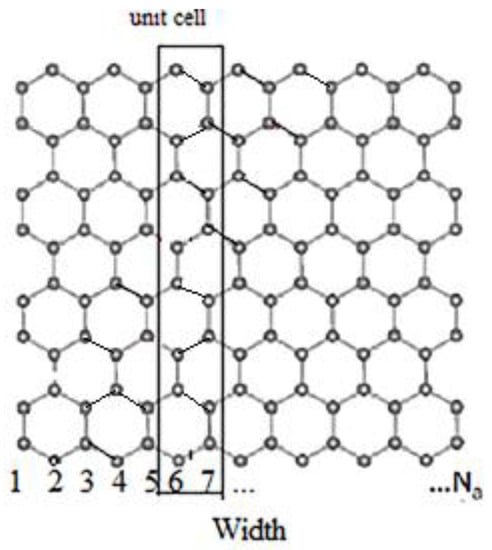
Figure 1.
An armchair GNR with the 1-D unit cell; Na is the number of dimer lines.
2.2. Green’s Function and Current–Voltage Derivation
The quantum ballistic transport through graphene-based FET by NEGF approach is considered in this section [17,23]. The main quantity in the NEGF theory is the Green’s function as:
where δ is an infinitesimal value in order to provide non-vanishing DOS at the Dirac point for the source/drain channel contacts [24,25].
The contacts’ self-energies is yielded by solving, where is the Green function related to drain/source contact. According to the Dirac formalisms [22] and tight-binding [26], a closed-form for is yielded as:
At last, the current through the drain/source contact can be computed by:
Here, : the LDOS, : filling function, : the Fermi function, : electron correlation function, and is the contact-broadening factor. Additionally, G and can be computed by the recursive Green function method since the Hamiltonian is a tridiagonal matrix [27].
2.3. Electrostatics
Suitable treatment of electrostatics is essential to yielding self-consistent potential, U(r), for precisely analyzing the GFET characteristics according to NEGF formalism. In a self-consistent approach, Poisson’s equation is solved to yield the potential field caused by a given electric charge. Then, this computed potential is applied as the input to NEGF, and an electric charge is obtained. Since the ballistic assumption in graphene-based elements yields one-dimensional transportation, the potential field is constant along the device width; therefore, the Poisson’s equation becomes a two-dimensional problem along the length and height of the channel and can be written as:
Here, q: electron charge, ε: dielectric constant, and Q(x): the charge density along the length of graphene, as:
where and are the source and drain LDOS, respectively.
The solving of the transport equations with Poisson’s equation, which accounts for electron–electron interactions through a potential U is shown in Figure 2.
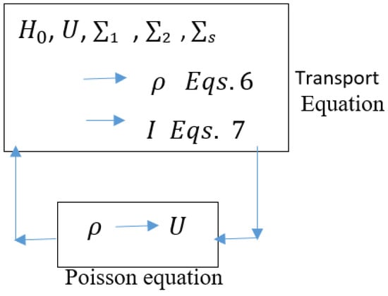
Figure 2.
Self-consistent solution of NEGF and Poisson’s Equation.
2.4. Physical-Based AVS Model
Since the energy gap in graphene is zero, the current in the AVS model for GFET has two parts due to electron and hole concentrations:
Injection velocity was computed using the least-squared curve-fitting routine [18]. is empirically derived to conduct the transition from the triode to the active region of transfer and output characteristics and is computed as:
where μ is mobility, is the GFET channel length, , , and are the intrinsic drain-source, gate-source, and drain-gate bias, respectively, and computed as voltage drop of the circuit shown in Figure 3.
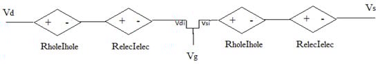
Figure 3.
A phenomenological AVS circuit model.
The electron and hole concentrations are given as:
where is minimum background doping, n is the subthreshold slope of GFET, and , electron and hole threshold, respectively, are computed by:
where shows the Diac-point voltage.
Here, α gives the shift in the threshold voltage, T/q = 0.0258*/298, is the thermal voltage, ΔV shows the trap charging on the graphene channel, and is the electron and hole inhomogeneity near the Dirac point in graphene, as:
where is gate capacitance, and is the non-ideality factor. In the proposed method, some of these parameters are optimized according to the NEGF algorithm, and special features compatible with graphene/DNA effects are chosen for biosensor modeling.
3. Results
This section shows some instances where in the proposed compact model can be used in healthcare fields to realize the response of GFET that is functionalized as a receptor of biological markers, such as DNA from living cells. First, the proposed transport model, based on NEGF, is simulated and verified by comparing with Low’s approach [15]. Then, eight parameters of the physical-based AVS model are optimized according to NEGF’s derived data. The effect of different variables on GFET transfer function are tested and compared with experimental results of DNA biomolecules and their effect on the graphene surface; four parameters of AVS are chosen. Then, these parameters are optimized by a least-square curve-fitting optimization algorithm according to experimental data to yield the AVS model as a DNA biosensor.
3.1. Simulation of GFET
To simulate the band structure of honeycomb graphene lattice, a proper unit cell, Figure 1, with the nearest neighbor approximation is chosen to compute the Hamiltonian matrix, h(k). Then, h(k) eigenvalues are extracted as energy for different values of k. The simulated results show the energy dispersion of Bulk Graphene has no bandgap, and the conduction and valence bands touch each other. The metallic nature and ambipolar conduction of the bulk graphene are due to its zero bandgap. There are six points of high symmetry in the band structure of bulk graphene at = (0, ±2π/3), (±π, ±π/3) as observed from Figure 4, so the bandgap is zero at these points. The E–k relationship around of the high symmetry points is almost linear, that shows the ‘nearly massless’ nature of electron in graphene. Additionally, the simple tight-binding model predicts that Zigzag GNR (ZGNR) has no bandgap, regardless of its width. The band structure of wide ZGNR looks similar to that of bulk graphene quantized along the axis, Figure 5a. Narrow Armchair GNR (AGNR) has a bandgap similar to semiconductors for particular values of the number of armchairs, Na, so it can be used as a semiconductor to create graphene-based FET, Figure 6.
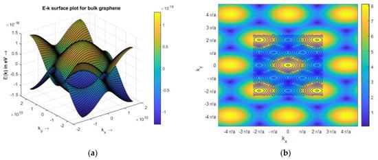
Figure 4.
Band structure of graphene. (a) E–K surface plot for bulk graphene; (b) contour plot of conduction band.
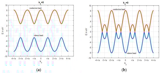
Figure 5.
Energy dispersion. (a) Energy versus (); (b) energy versus ().
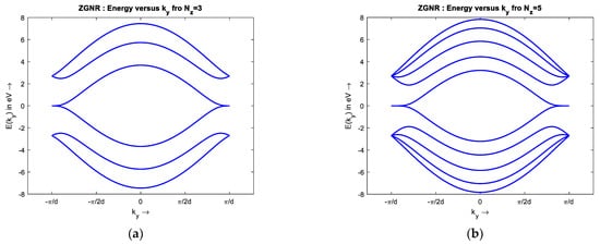
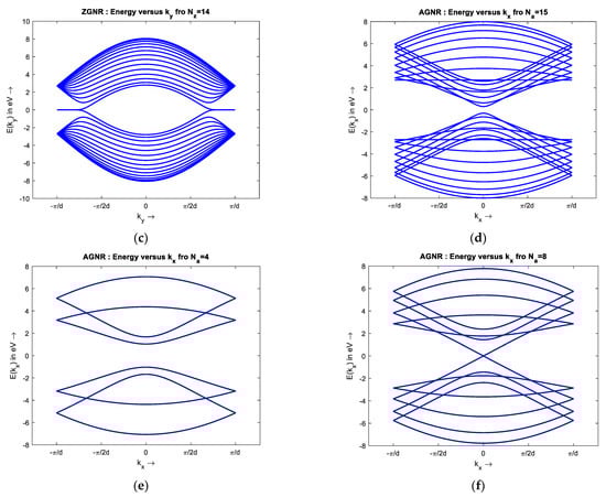
Figure 6.
Band structure of (a–c) ZGNR, Nz = 3, 5, 14, and (d–f) AGNR, Na = 15, 4, and 8.
The bandgap of AGNR for armchair number, = 3l; + 2; l integer, loses its semiconducting properties and becomes metallic. Additionally, the bandgap of AGNR decreases with increasing width. The band structure of wide AGNR looks similar to that of bulk graphene sampled along the . axis (Figure 5b).
3.2. NEGF Modeling of GFET
To simulate devices, the graphene FET at IBM with gate length 40 nm is used [28], when the gate oxide is with an oxide thickness of 10 nm. The pure graphene channel length is 40 nm, and the metals of drain and source are palladium. GFET potential values and corresponding transmission spectrum of the proposed method agree well with Low’s method [15], as shown in Figure 7. Figure 7 shows the transmission that is contributed by the thermionic current, the source-channel, and the channel-drain tunneling current. The transmission is non-zero for all energies, which shows the device is gapless, but there are minimum values that separate the regions in the transmission spectrum. According to and shown in Figure 8, for negative and positive Values the negative differential resistance (NDR) and positive resistance appeared, respectively. These effects in current/voltage characteristics are agreed well with other simulations [29,30,31] and experimental results [32,33]. The above results show that the formalization and assumptions considered for GFET are acceptable.
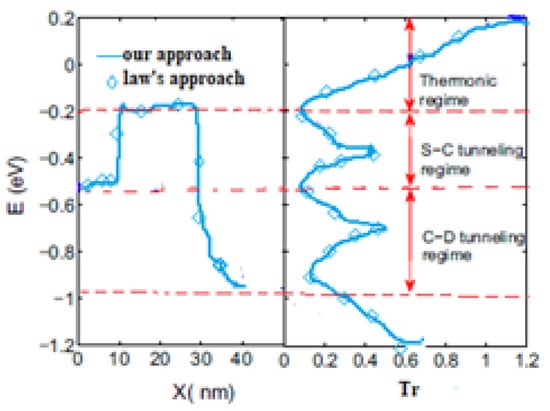
Figure 7.
GFET potential profile and corresponding transmission spectra of GFET; proposed method (solid line), and proposed approach (circles).
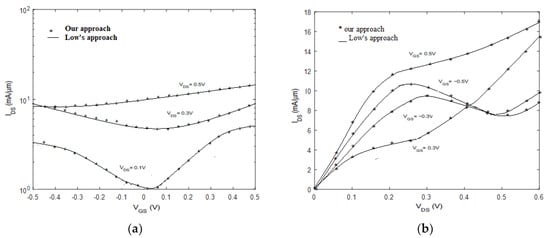
Figure 8.
(a) Transfer characteristics. (b) Output characteristics of GFET, proposed method (solid line), and low’s approach (circles).
3.3. Physical-Based AVS Model Parameter Optimization
To create an appropriate biosensor model, the extracted data from NEGF modeling are used to determine AVS model parameters that are compatible with GFET characteristics. In the first step, the training data file provided by the proposed NEGF approach is formed in a three-column format. The first column corresponds to the drain-source bias, , the second column corresponds to the gate-source bias, , while the third column is the measured drain-source current, , in Amperes per meter of the device width. Then, MATLAB’s built-in routine least-square curve-fitting routine, lsqcurvefit, is used to optimize the parameters in the AVS model according to the training file. In the used AVS v1.0.0 circuit model [34], the fixed parameters are shown in Table 1, and a total of eight parameters can be optimized as shown in Table 2. In order to extract a realistic and physically meaningful way, all the optimized parameters are considered with appropriate lower and upper bounds, including a robust initial guess. Table 2 shows the extracted parameters with their lower and upper bounds and initial guess values used in the nonlinear parameter extraction routine. After optimizing AVS parameters, a good agreement is yielded with NEGF results; Figure 9.

Table 1.
Fixed parameters in the AVS v1.0.0. model.
Table 2.
Parameters in the AVS v1.0.0 model that are extracted upon calibration with NEGF data.
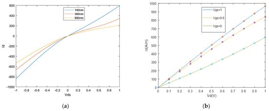
Figure 9.
(a) Output characteristics of 140-300-650 nm device. (b) Output characteristics of 40 nm device. NEGF data are shown in symbols, while solid lines show the GFET model fits by AVS.
3.4. Biosensor Modelling by AVS Model
In this section, the general sensing system operation pattern is explained and applied to biological samples. Specifically, the physical properties of GFET are influenced by the charge magnitude and/or dipole moment of DNA molecules attached to the surface of graphene. Figure 10 shows the GFET transfer characteristic with its related physical phenomena. When DNA molecules are bound by receptors attached to the graphene surface, positive or negative charges transfer between them depending on the energy dispersion, and the neutral point shifts, as shown in Figure 10a. Additionally, the hole and electron mobility is influenced by the Coulomb potential to produce a slope change in the hole and electron branch of the profile, respectively, as shown in Figure 10b,c. Additionally, the minimum conductivity changes at the near of NP due to modulation of residual carriers and/or charged impurities by DNA molecules, as shown in Figure 10d. Therefore, it is possible to model these four effects by similarity parameters of the AVS model as the electron branch resistance , the hole branch resistance , injection velocity carrier and Dirac-point voltage . The DNA-specific information and its effects on GFET can be characterized within a feature space, as shown in Figure 11.
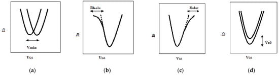
Figure 10.
DNA molecule effects on Ids/Vgs profile of GFET. (a) Charge-neutral point movement; (b) the hole branch slope changing due to the DNA molecule; (c) the electron branch slope changing due to the DNA molecule; (d) the height changing of the charge-neutral point due to DNA molecules.
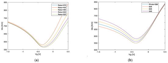
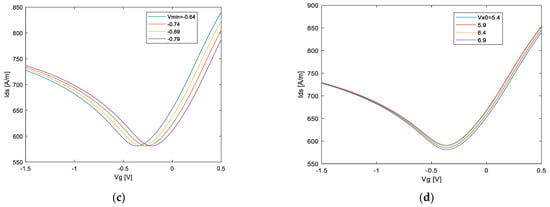
Figure 11.
Schematic illustration of different parameter effects of AVS model. and .
To optimize the proposed AVS parameters according to experimental data, the results in [35] are considered. Probe DNAs (5′-AGG-TCG-CCG-CCC-SH-3′) with a high concentration (1 mM in 40 mL PBS buffer), complementary (3′ TCC-AGC-GGC-GGG-5′), and one-base mismatched (3′ TCC-AGC-GGC-GTG-5′) DNAs were used in [35]. In [35], the transfer profile, Id/Vgs, has been measured before and after the addition of probe DNA molecules, and after the addition of complementary and one-base mismatched DNAs, with different concentrations. The transfer curve, Id/Vgs, shows ambipolar behavior of GFET, as shown in Figure 12. The results show that the Vmin0 is left-shifted to the immobilization of probe DNAs and significantly left-shifted with the addition of complementary DNA molecules, proposing an n-doped GFET. Additionally, the minimum current at Vmin0 decreased by adding complementary DNAs concentration. Additionally, some changes are viewed in the resistors, the slope of lines, in ambipolar parts of electron and hole conduction area in the transfer curve. These experimental data are extracted for different cases, bare, DNA probe, and different concentrations of DNA and applied to the optimization algorithm to extract AVS model parameters. After training, the extracted parameters are used to yield transfer curves, as shown in Figure 12, that are in agreement with experimental data.
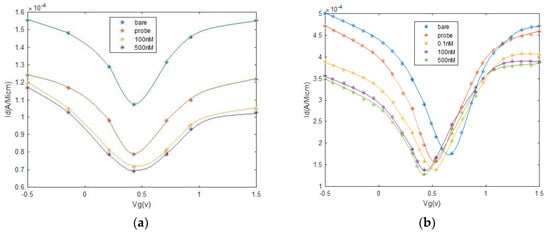
Figure 12.
Transfer characteristics for GFET–based biosensor, bare, with the probe, and after DNA reaction, at different concentrations. (a) Mismatched (b) and complementary DNAs. Experimental data are shown in symbols, while solid lines show the GFET–based biosensor model fits by AVS.
4. Conclusions
The interface between nanomaterials and biomolecules, such as Graphene/DNA, is growing for the electrical detection of different biomarkers of diseases. Specifically, sequence-selective GFET-based sensors have attracted much attention for genetic disease diagnosis in recent years. Most DNA sensors are implemented by optical or electrochemical transducers, which require their special labels, but label-free electrical detection of DNAs by GFET allows a sensitive and rapid measurement. In comparison to other nanomaterials, graphene is expected to excel due to its large surface-to-volume ratio, high conductance, biocompatibility, and ambipolar profile. In the proposed approach, according to the profile, four distinctive parameters were recognized in correspondence to the physical parameters of AVS models. These parameters are optimized by the least-square curve-fitting routine according to experimentally derived data. In the AVS model, the constant parameters are yielded from analytical formalization, and other variable parameters are extracted by optimization algorithms using NEGF’s data. The proposed compact model yields compatible characteristics with the physical phenomenon of the GFET/DNA molecule. The model can be easily used in the design and investigation of GFET biosensors for the detection of single-base polymorphism or mutation as an essential key to the hereditary infections diagnosis and personalized medicine realization.
Author Contributions
Conceptualization, M.A., M.J.S. and L.L.S.; methodology, M.A., M.J.S. and L.L.S.; software, M.A. and M.J.S.; validation, M.A., M.J.S., L.L.S. and A.K.; formal analysis, M.A., M.J.S., L.L.S. and A.K.; investigation, M.A., M.J.S., L.L.S. and A.K.; writing—original draft preparation, M.A., M.J.S.; writing—review and editing M.A., M.J.S., L.L.S. and A.K.; supervision, M.J.S., L.L.S. and A.K.; project administration, M.J.S. and L.L.S. All authors have read and agreed to the published version of the manuscript.
Funding
This research received no external funding.
Institutional Review Board Statement
Not applicable.
Informed Consent Statement
Not applicable.
Data Availability Statement
Not applicable.
Conflicts of Interest
The authors declare no conflict of interest.
Appendix A. Basic Concepts of Graphene
Appendix A.1. Basic Concepts of Graphene Band Structure
In the twentieth century, scientists confirmed Schrödinger’s Equation (A1) as a formal quantitative basis to calculate the energy levels for any confining potential as:
where , , , and Ψ show the Planck constant, the mass of an electron, confined potential, and wave function of the electron, respectively. After solving this equation, Ψ is used to extract other electrical parameters, such as gives the presence probability of electron in a volume of dv and adds it up for all the electrons is used to obtain average electron density . Additionally, the current density probability is obtained as:
Schrödinger’s equation can be solved when the self-consistent potential U(r) is yielded from Poisson’s Equation (A3).
Analytical modeling of a device in equilibrium generally requires an iterative solution of Equations (A1) and (A3). These equations for simple material structures and boundaries can be solved analytically, but most practical problems require a numerical solution. In numerical models such as finite-difference, the Partial Differential Equation (PDE) is converted to matrix equation as:
where is the wave function value around lattice points i at time t.
Additionally, the second derivative must be turned into a difference equation:
Therefore:
where .
The solution of Equation (4) becomes any superposition :
So the eigenvalues energy dispersion, and eigenvectors of H are extracted from:
That is known as the time-independent Schrödinger equation.
This approach can be used for calculating the band structure of any periodic solid, such as graphene, with an arbitrary number of atoms per unit cell. In the general procedure, the reciprocal lattice in the k-space is constructed. In this case, any point on the direct lattice can be shown as:
where ,, and are integers and , , and are lattice basis vectors.
Then, the points on the reciprocal lattice can be written as Equation (A10), where M, N, P are integers.
The basis vectors of the reciprocal lattice , , and are constructed according to the external and internal product, as:
The above relations are used to yield reciprocal space for energy dispersion extraction of graphene in the proceeding sections.
Appendix A.2. Two-Dimensional Energy Band Structure of Single-Layer Graphene
Graphene is constructed from carbon atoms bonded in the hexagonal 2D plane as in the honeycomb lattice (Figure A1).
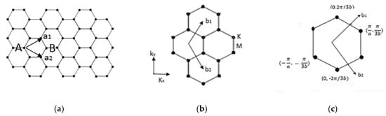
Figure A1.
Single-layer graphene. (a) Real space and , basis vectors; (b) reciprocal space and , basis vectors; (c) Brillouin zone.
The basis vectors in real space, , and reciprocal vectors, , are shown in Figure A1 and calculated as:
where , is carbon–carbon atom distance, and diamond contains A and B shows the unit cell.
Because we have two atoms in the unit cell, the Hamiltonian matrix is a 2 × 2 matrix [16,17]:
The unit cell, shown in Figure A2, is A1 and B1, so B2, B3, A3, and A2 are the nearest atoms of its neighbor cells.
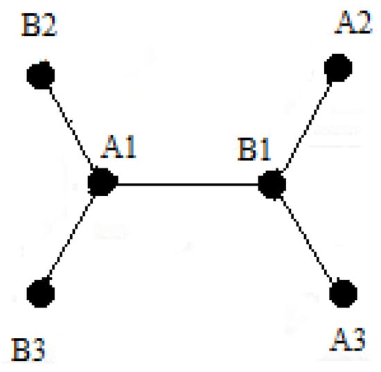
Figure A2.
Graphene cell (A1 and B1) and its neighbors.
Where the Hamiltonian matrix is computed as the equation represented in the previous section, and for this case is formalized as below.
Thus, is yielded as:
where:
Additionally, eigenvalues are computed for extracting energy dispersion, as:
where
The energy dispersion for , t = −3.033 ev, and s = 0.129 is shown in Figure A3.
Figure A3.
Energy dispersion. (a) A 3D band structure; (b) 2D band structure in the high symmetry point route.
By Slater-Koster [16] approximation s = 0, the dispersion equation becomes:
If other orbitals such as , 2, 2, and 2 were considered, the Hamiltonian matrix becomes 8 × 8, so eight eigenvalues are shown in Figure A4.
Figure A4.
Energy dispersion for 2s, 2px, 2py, and 2pz. (a) Different orbits of graphene; (b) valence and conductance band; (c) energy dispersion of different orbits of graphene.
Additionally, for the three nearest neighbors, the dispersion energy is shown in Figure A5.
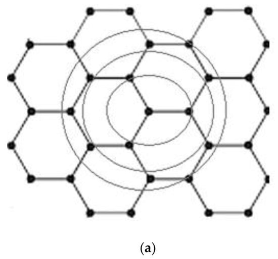
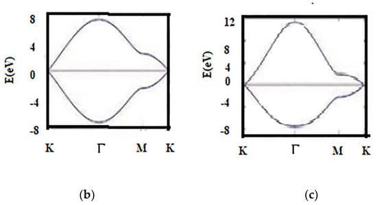
Figure A5.
Energy dispersion with 3 nearest neighbors. (a) Three nearest neighbors (3N-N); (b) band energy comparison for N-N; (c) 3N-N.
References
- Sheikhzadeh, E.; Eissa, S.; Ismail, A.; Zourob, M. Diagnostic techniques for COVID-19 and new developments. Talanta 2020, 220, 121392. [Google Scholar] [CrossRef]
- Singh, S.; Kumar, V.; Dhanjal, D.S.; Datta, S.; Prasad, R.; Singh, J. Biological Biosensors for Monitoring and Diagnosis. Microb. Biotechnol. Basic Res. Appl. 2020, 317–335. [Google Scholar] [CrossRef]
- Rawat, B. Royy Pally: Modeling of graphene-based field-effect transistors through a 1-D real-space approach. J. Comput. Electron. 2018, 17, 90–100. [Google Scholar] [CrossRef]
- Novoselov, K.S.; Falko, V.I.; Colombo, L.; Gellert, P.R.; Schwab, M.G.; Kim, K. A roadmap for graphene. Nature 2012, 490, 192. [Google Scholar] [CrossRef]
- Wu, G.F.; Tang, X.; Meyyappan, M.; Lai, K.W.C. Doping effects of surface functionalization on graphene with aromatic molecule and organic solvents. Appl. Surf. Sci. 2017, 425, 713–721. [Google Scholar] [CrossRef]
- Akbari, E.; Buntat, Z.; Nilashi, M.; Afroozeh, A.; Farhange, Y.; Zeinalinezhad, A. ISVR modeling of an interferon gamma (IFN-) biosensor based on graphene. Anal. Methods 2016, 8, 7217–7224. [Google Scholar] [CrossRef]
- Karimi, H.; Rahmani, R.; Mashayekhi, R.; Ranjbari, L.; Shirdel, A.H.; Haghighian, N.; Movahedi, P.; Hadiyan, M.; Ismail, R. Analytical development and optimization of a graphene-solution interface capacitance model. Beilstein J. Nanotechnol. 2014, 5, 603–609. [Google Scholar] [CrossRef] [Green Version]
- Karimi, H.; Yusof, R.; Rahmani, R.; Hosseinpour, H.; Ahmadi, M.T. Development of solution-gated graphene transistor model for biosensors. Nano Res. Lett. 2014, 9, 71–78. [Google Scholar] [CrossRef] [PubMed] [Green Version]
- Logoteta, D.; Marconcini, P.; Bonati, C.; Fagotti, M.; Macucci, M. High-performance solution of the transport problem in a graphene armchair structure with a generic potential. Phys. Rev. E Stat. Nonlin. Soft Matter Phys. 2014, 89, 063309. [Google Scholar] [CrossRef] [PubMed] [Green Version]
- Wu, G.F.; Tang, X.; Lin, Z.H.; Meyyappan, M.; Lai, K.W.C. The effect of ionic strength on the sensing performance of liquid-gated biosensors. In Proceedings of the IEEE 17th International Conference on Nanotechnology (IEEE-NANO), Pittsburgh, PA, USA, 25–28 July 2017; pp. 242–245. [Google Scholar]
- Wu, G.F.; Dai, Z.W.; Tang, X.; Lin, Z.H.; Lo, P.K.; Meyyappan, M.; Lai, K.W.C. Graphene field-effect transistors for the sensitive and selective detection of Escherichia coli using pyrene-tagged DNA aptamer. Adv. Healthc. Mater. 2017, 6, 1700736. [Google Scholar] [CrossRef]
- Pourasl, A.H.; Ahmadi, M.T.; Rahmani, M.; Ismail, R. Graphene Based Biosensor Model for Escherichia Coli Bacteria Detection. J. Nanosci. Nanotechnol. 2017, 17, 601–605. [Google Scholar] [CrossRef] [PubMed]
- Ushiba, S.; Okino, T.; Miyakawa, N.; Ono, T.; Shinagawa, A.; Kanai, Y.; Inoue, K.; Takahashi, K.; Kimura, M.; Matsumoto, K. State-space modeling for dynamic response of graphene FET biosensors. Jpn. J. Appl. Phys. 2020, 59, SGGH04. [Google Scholar] [CrossRef]
- Fiori, G.; Iannaccone, G. 3D Poisson/NEGF Solver for the Simulation of Graphene Nanoribbon, Carbon Nanotubes and Silicon Nanowire Transistors. NanoTCAD ViDES. 2016. Available online: https://nanohub.org/resources/vides (accessed on 30 April 2021).
- Low, T.; Hong, S.; Appenzeller, J.; Datta, S.; Lundstrom, M. Conductance asymmetry of graphene p-n junction. IEEE Trans. Electron. Dev. 2009, 56, 1292. [Google Scholar] [CrossRef] [Green Version]
- Datta, S. Nanoscale device modeling: The Green’s function method. Superlattices Microstruct. 2000, 28, 253. [Google Scholar] [CrossRef]
- Datta, S. Electronic Transport. In Mesoscopic System; Cambridge University Press: Cambridge, UK, 1995. [Google Scholar]
- Coleman, T.; Li, Y. An interior trust region approach for nonlinear minimization subject to bounds. SIAM J. Optim. 1996, 6, 418–445. [Google Scholar] [CrossRef] [Green Version]
- Zhao, P.; Guo, J. Modeling edge effects in graphene nanoribbon field-effect transistors with real and mode space methods. J. Appl. Phys. 2009, 105, 034503. [Google Scholar] [CrossRef] [Green Version]
- Wallace, P.R. The band theory of graphite. Phys. Rev. 1947, 71, 622–634. [Google Scholar] [CrossRef]
- Saito, R.; Dresselhaus, G.; Dresselhaus, M.S. Physical Properties of Carbon Nanotubes; Imperial College Press: London, UK, 1998. [Google Scholar]
- Brey, L.; Fertig, H.A. Electronic states of graphene nanoribbons studied with the Dirac equation. Phys. Rev. B Condens. Matter 2006, 73, 235–411. [Google Scholar] [CrossRef] [Green Version]
- Haug, H.; Jauho, A.P. Quantum Kinetics in Transport and Optics of Semiconductors; Springer Series in Solid State Sciences; Springer: New York, NY, USA, 1996; p. 123. [Google Scholar]
- Schomerus, H. Effective contact model for transport through weaklydoped graphene. Phys. Rev. B Condens. Matter 2007, 76, 45–433. [Google Scholar] [CrossRef] [Green Version]
- Mojarad, R.G.; Datta, S. Effect of Contact Induced States on Minimum Conductivity in Graphene. Phys. Rev. B 2009, 79, 085410. [Google Scholar] [CrossRef] [Green Version]
- Zheng, H.; Wang, Z.F.; Luo, T.; Shi, Q.W.; Chen, J. Analytical study of electronic structure in armchair graphene nanoribbons. Phys. Rev. B Condens. Matter 2007, 75, 165–414. [Google Scholar] [CrossRef] [Green Version]
- Lake, R.; Klimeck, G.; Brown, R.C.; Jovanovic, D. Single and multiband modeling of quantum electron transport through layered semiconductor devices. J. Appl. Phys. 1997, 81, 7845–7869. [Google Scholar] [CrossRef] [Green Version]
- Wu, Y.; Jenkins, K.A.; Valdes-Garcia, A.; Farmer, D.B.; Zhu, Y.; Bol, A.A.; Dimitrakopoulos, C.; Zhu, W.; Xia, F.; Avouris, P.; et al. State-ofthe-art graphene high-frequency electronics. Nano Lett. 2012, 12, 3062–3067. [Google Scholar] [CrossRef]
- Ganapathi, K.; Yoon, Y.; Lundstrom, M.; Salahuddin, S. Ballistic I-V characteristics of short-channel graphene field-effect transistors: Analysis and optimization for analog and RF applications. IEEE Trans. Electron. Dev. 2013, 60, 958. [Google Scholar] [CrossRef]
- Grassi, R.; Low, T.; Gnudi, A.; Baccarani, C. Contact-induced negative differential resistance in short-channel graphene FETs. IEEE Trans. Electron. Dev. 2013, 60, 140. [Google Scholar] [CrossRef] [Green Version]
- Grassi, R.; Gnudi, A.; Di Lecce, V.; Gnani, E.; Reggiani, S.; Baccarani, G. Exploiting negative differential resistance in monolayer graphene FETs for high voltage gains. IEEE Trans. Electron. Dev. 2014, 61, 617. [Google Scholar] [CrossRef] [Green Version]
- Meric, I.; Han, M.Y.; Young, A.F.; Ozyilmaz, B.; Kim, P.; Shepard, K.L. Current saturation in zero-bandgap, top-gated graphene fieldeffect transistors. Nat. Nanotechnol. 2008, 3, 654. [Google Scholar] [CrossRef]
- Han, S.J.; Reddy, D.; Carpenter, G.D.; Franklin, A.D.; Jenkins, K.A. Current saturation in submicrometer graphene transistors with thin gate dielectric: Experiment, simulation, and theory. ACS Nano 2012, 6, 5220. [Google Scholar] [CrossRef]
- Rakheja, S.; Antoniadis, D. Ambipolar Virtual Source Compact Model for Graphene FETs. Available online: https://nanohub.org/publications/10 (accessed on 23 October 2014).
- Dong, X.; Shi, Y.; Huang, W.; Chen, P.; Li, L.J. Electrical Detection of DNA Hybridization with Single-Base Specificity Using Transistors Based on CVD-Grown Graphene Sheets. Adv. Mater. 2010, 22, 1649–1653. [Google Scholar] [CrossRef]
Publisher’s Note: MDPI stays neutral with regard to jurisdictional claims in published maps and institutional affiliations. |
© 2021 by the authors. Licensee MDPI, Basel, Switzerland. This article is an open access article distributed under the terms and conditions of the Creative Commons Attribution (CC BY) license (https://creativecommons.org/licenses/by/4.0/).