Article

Design of Inverted Nano-Cone Arrayed SERS Substrate for Rapid Detection of Pathogens

1
Department of Mechanical Engineering, Massachusetts Institute of Technology, 77 Massachusetts Avenue, Cambridge, MA 02139, USA
2
Department of Chemistry, College of Science, Imam Abdulrahman Bin Faisal University, P.O. Box 1982, Dammam 31441, Saudi Arabia
3
Biophysics Research Epidemic Research Department, Institute for Medical and Consultations (IRMC), Imam Abdulrahman Bin Faisal University, P.O. Box 1982, Dammam 31441, Saudi Arabia
4
Biology Department, College of Science, Imam Abdulrahman Bin Faisal University, P.O. Box 1982, Dammam 31441, Saudi Arabia
*
Author to whom correspondence should be addressed.
Appl. Sci. 2021, 11(17), 8067; https://doi.org/10.3390/app11178067
Submission received: 19 July 2021 / Revised: 17 August 2021 / Accepted: 25 August 2021 / Published: 31 August 2021
(This article belongs to the Special Issue Recent Advances and Future Trends in Nanophotonics Ⅱ)

Abstract

:

Featured Application

This work reports a new design of surface-enhanced Raman spectroscopy (SERS) substrate which will provide high enough sensitivity and fast and close contact of the target structure to the optical hot spots with an enhancement factor of 108 or higher, which could be high enough to detect immunomagnetically densified bacteria.

Abstract

Rapid detection of bacteria is a very critical and important part of infectious disease treatment. Sepsis kills more than 25 percent of its victims, resulting in as many as half of all deaths in hospitals before identifying the pathogen for patients to get the right treatment. Raman spectroscopy is a promising candidate in pathogen diagnosis given its fast and label-free nature, only if the concentration of the pathogen is high enough to provide reasonable sensitivity. This work reports a new design of surface-enhanced Raman spectroscopy (SERS) substrate which will provide high enough sensitivity and fast and close contact of the target structure to the optical hot spots for immunomagnetic capturing-based bacteria-concentrating technique. The substrate uses inverted nanocone structure arrays made of transparent PDMS (Polydimethylsiloxane) to funnel the light from the bottom to the top of the cones where plasmonic gold nanorods are located. A high reflective and low loss layer is deposited on the outer surface of the cone. Given the geometry of cones, photons are multi-reflected by the outer layer and thus the number density of photons at hotspots increases by an order of magnitude, which could be high enough to detect immunomagnetically densified bacteria.

1. Introduction

Rapid detection of bacterial infection is a very critical and urgent part of infectious disease diagnostics and treatment. Sepsis kills more than 25 percent of its victims and costs hospitals billions of dollars annually. In the U.S. alone, more than a million people become infected each year, resulting in as many as half of all deaths in hospitals [1,2]. But the diagnosis of sepsis takes possibly up to five days to cultivate and identify bacteria in current clinical standards [3,4]. This need of novel diagnosis tools pushes forward the development of biosensors. Many biosensors have been developed to detect bacteria in blood, serum, water, foods and biofilms. Several biomaterials (enzymes, antibodies, DNA and lectin) are used to identify a target molecule and produce perceptible signals detectable by a transducer.
Surface Enhanced Raman Spectroscopy (SERS) is a label-free-based optical biosensor, utilizing a modified form of Surface Plasmon Resonance (SPR). In Raman spectroscopy, as laser light interacts with a sample, the light will be scattered inelastically [5,6,7]. During this process, the inelastic scattering of incident photons [8,9] can change wavelength according to the vibrational modes of the molecules. This difference of wavelength between incident and scattered photons provides rich vibrational information about the chemical bonds. Practically, it can also provide a high spatial resolution [10]. To improve and enhance Raman signals, SERS employs metallic nanomaterials, like a SERS tag. A SERS tag consists of modified metallic nanoparticles with specific capturing probes or Raman reporter molecules. This approach provides a high sensitivity approach with multiplexing potentials.
The crucial task to employ SERS into low concentration bio-sensing is to increase the intensity of the vibration mode, I S E R S , by enhancing the electric field at the location of the sensing [11]:
I S E R S E λ E 0 λ 2 E λ s E 0 λ s 2
where λ is the incident wavelength and λ s is the Raman scattering wavelength, E is the local electric field intensity, and E0 is the incident electric field intensity. Since the frequency shift due to Raman scattering is small compared to the incident wavelength, the enhancement factor (EF) can be written as [12]:
E F   E λ E 0 λ 4
With a given order of magnitude enhancement on light field, the signal output of a substrate is:
I E F × N m o l e c u l e
where N m o l e c u l e represents the number of molecules in contact with plasmonic “hot-spots”.
The most common way to improve the EF factor of a substrate is to use plasmonic material that supports Localized Surface Plasmon Resonance (LSPR) [7]. In LSPR, the surface plasmon will bond the photon close to the surface of metal, confine the light field in a short range and increase light field intensity. However, the LSPR made by the deposition process has an EF factor far from perfect. In a typical sepsis detection, when the concentration of bacteria in sepsis patients is as low as 1–100 CFU/mL, the pathogen has to be enriched by a factor of 105 to perform Raman measurement [13,14]. In this situation, the state-of-the-art Raman enhancement approach is to increase the intensity of the local electromagnetic environment.
For example, Weisheng et al. [15] placed gold dimers on a metallic surface. The metallic surface generates plasmon and confined light fields. The dimers take the photons from a concentrated light field and the EF is around 105. Masahiko et al. [16] use an Au disc array on a dielectric-metal-quartz substrate. The periodic disc array scatters lights into a wave pack whose wavevector matches the plasmon mode between dielectric and metal, and photons are trapped and delivered to the discs. In this work, the EF rises to 106. Dongzhi et al. [17] reported deposited metal film on oxidized porous Al. The Al2O3 layer between substrate and metal film will work as the resonator that traps the light, and thus increases the EF made by the metal film at the top of the structure. The EF in this work is around 104. Another method needs to be proposed to improve EF.
Immunocapturing is a method for bacterial capturing from complex samples by applying specific probes or antibodies targeting specific regions of the bacteria [18]. If the probes are decorated on magnetic beads that can be collected by an external magnetic field, it will allow 2–3 orders of magnitude enrichment of bacteria. It is known as immunomagnetic capturing [19,20,21]. The antibiotic modified magnetic bead will bind to the bacteria. Then the bacteria-bead cluster can be collected by applying a magnetic field. The captured bacteria will be delivered to Raman substrate (the substrate approach) [15,16,17], or directly bound with plasmonic nanoparticles (the colloidal approach) [19,20,21]. The colloidal approach is to excite the LSPR of particles, whose EF is limited within 106. As discussed before, even with the assistance of ordered surface structure, the EF in substrate can hardly be higher than 106. Even with the assistance of immunomagnetic capturing, to perform rapid, non-culturing detection of bacteria, the Raman sensor sensitivity should be improved 2 more orders of magnitude. Unfortunately, the current Raman measurement cannot fill this sensitivity gap. The second concern is the blocking of incident light in current Raman measuring setups. In colloidal methods, bead, bacteria and nano metal particles are randomly bound to each other, and incident light can be blocked by the target cells instead of reaching plasmonic materials. For the substrate approach, bacteria will sit at the top of the plasmonic surface, and incident light will come from top to bottom and a large portion of incident light will be blocked and absorbed by the target bacteria.

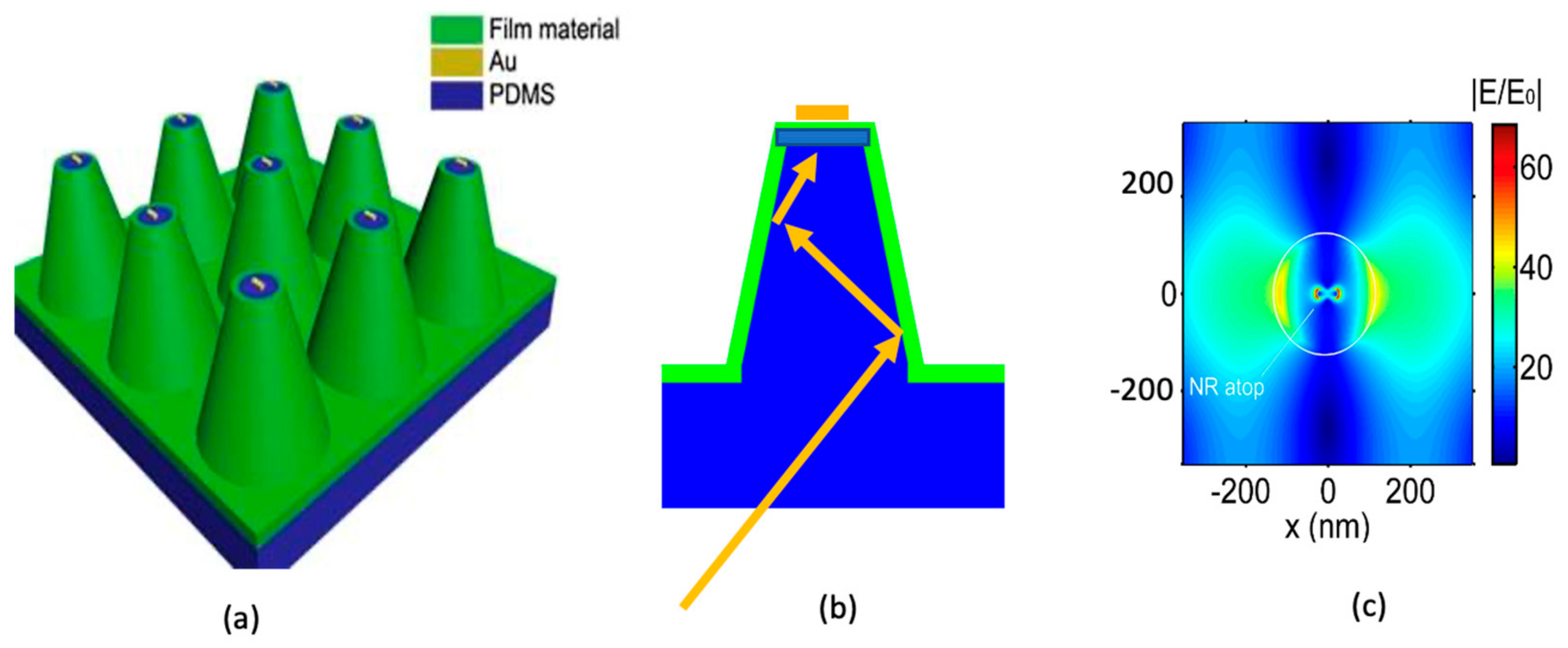
2. Photon Funneling Inverted Nanocone Design and Numerical Analysis

The SERS substrate array proposed in this work can address the aforementioned issues. The substrate is made up of transparent cones where the radius decreases along the light path. A high reflective and low loss layer is deposited on the outer surface of the cone. Given the geometry of cones, photons are multi-reflected by the outer layer and thus the number density of photons increases by 4 to 7 times. When this higher concentration of “photon gas” reaches the plasmonic metal, the Raman signal enhancement can be as high as 108. The substrate is designed to allow light to come from the bottom of the transparent nanostructures and has no photon blocking problem.
The incident photons are multi-reflected inside the cavity, known as cavity resonance [22]. This resonance mode can trap the light and concentrate it. In this work, the photon-capturing cavity structure is used to promote the SERS, where the nanorod at the top is going to absorb those concentrated photons. The numerical method used in this paper is Finite-Difference Time-Domain (FDTD) method, done by FDTD Solution (Lumerical Inc., version 1.6, Vancouver, BC, Canada) with 3nm cubic mesh. In the simulation, 2-D arrays of meshes have been utilized as observing planes, and the SERS refers to the maximum field enhancement in the observing plane. The body of this substrate is made of Polydimethylsiloxane (PDMS), a transparent material that allows light to illuminate from bottom to top. A coating film is made at the surface of the substrate to promote the reflection of photons and will enable 108 EF. This substrate is illustrated as Figure 1. The enhancement effect only happens at the top surface of the cone, whose area is inevitably reduced because of the cavity sloping. Also, the gap between 2 cones should be large enough to locate the magnetic bead and will make the contact area even smaller. To have maximum relative signal output, the pattern and geometry of the substrate is optimized and will be discussed in Section 4 with more details. In the FDTD simulation, the structure is surrounded by water, and materials’ optical models are obtained from Palik’s book [23]. The structure is shown in Figure 2. The cone is made of PDMS, and the structure can be obtained by inverse molding of our previous cavity [14]. By pouring liquid PDMS onto the structure and letting it cool down, the microstructure pattern can be transferred into the new structure. The geometric features of the inverse cavity are bottom diameter 500 nm, top diameter 200 nm, height 1000 nm and periodicity 840 nm. This geometry will be optimized in the following section of the designing process.

3. Results

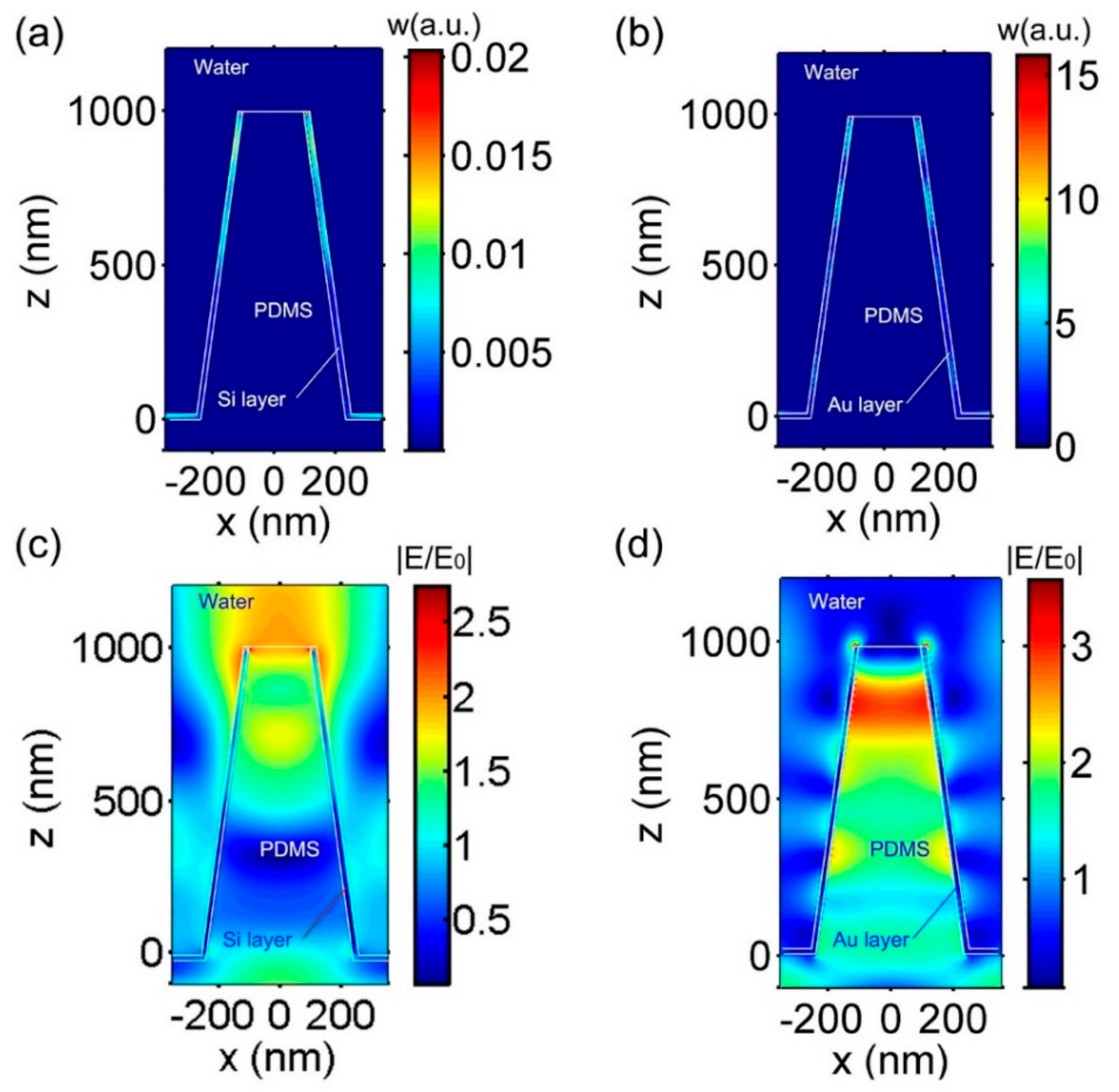
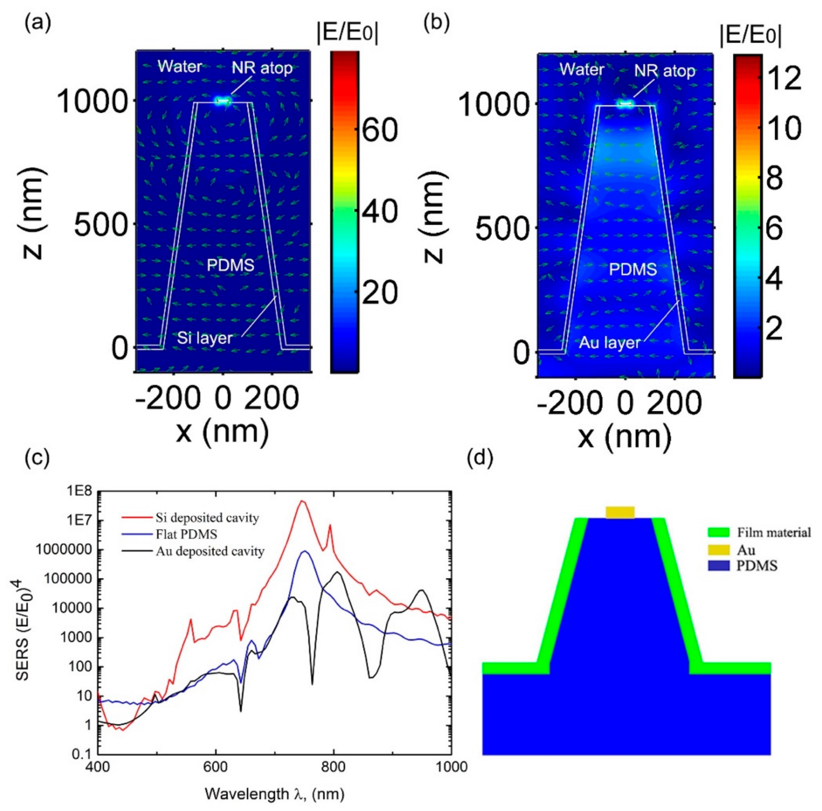
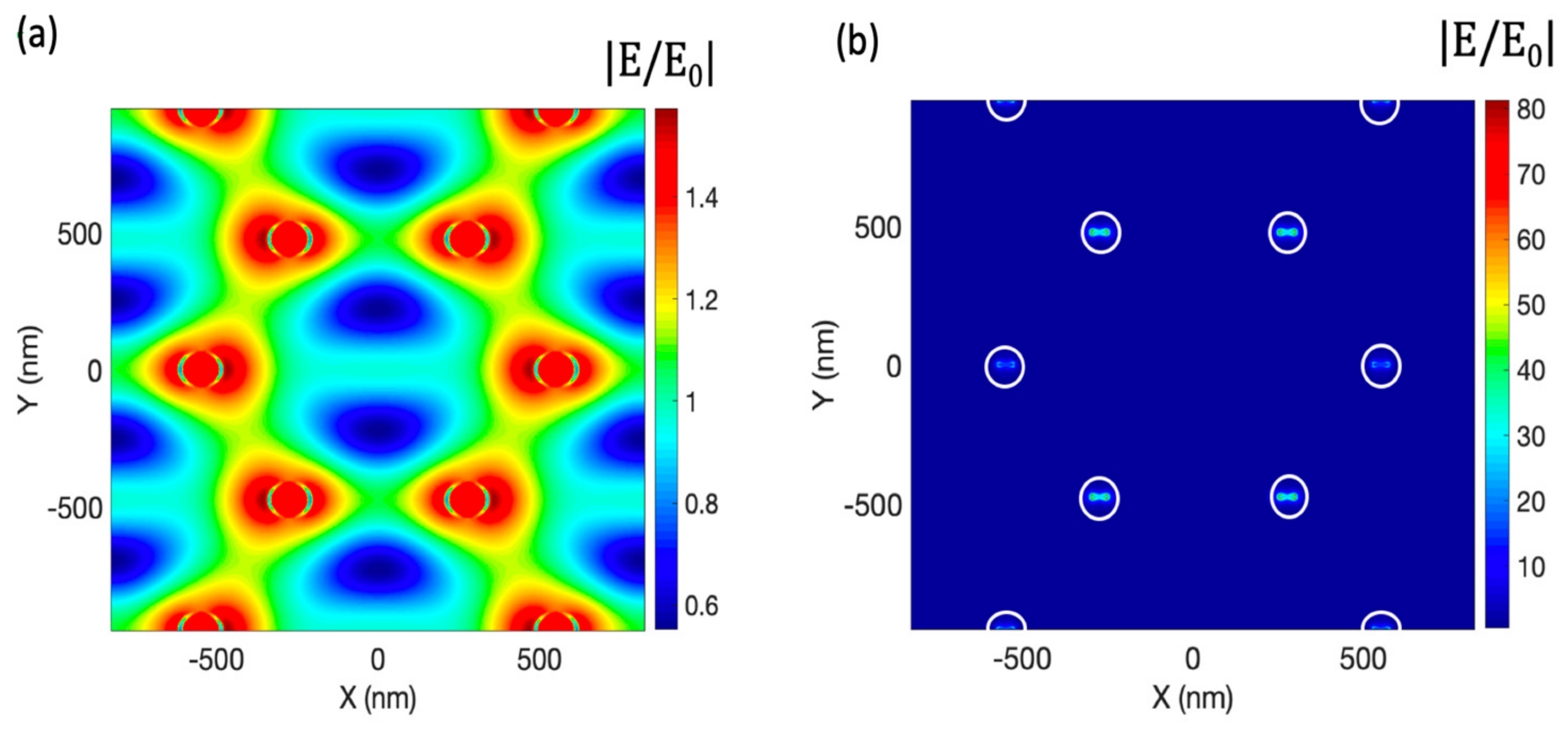
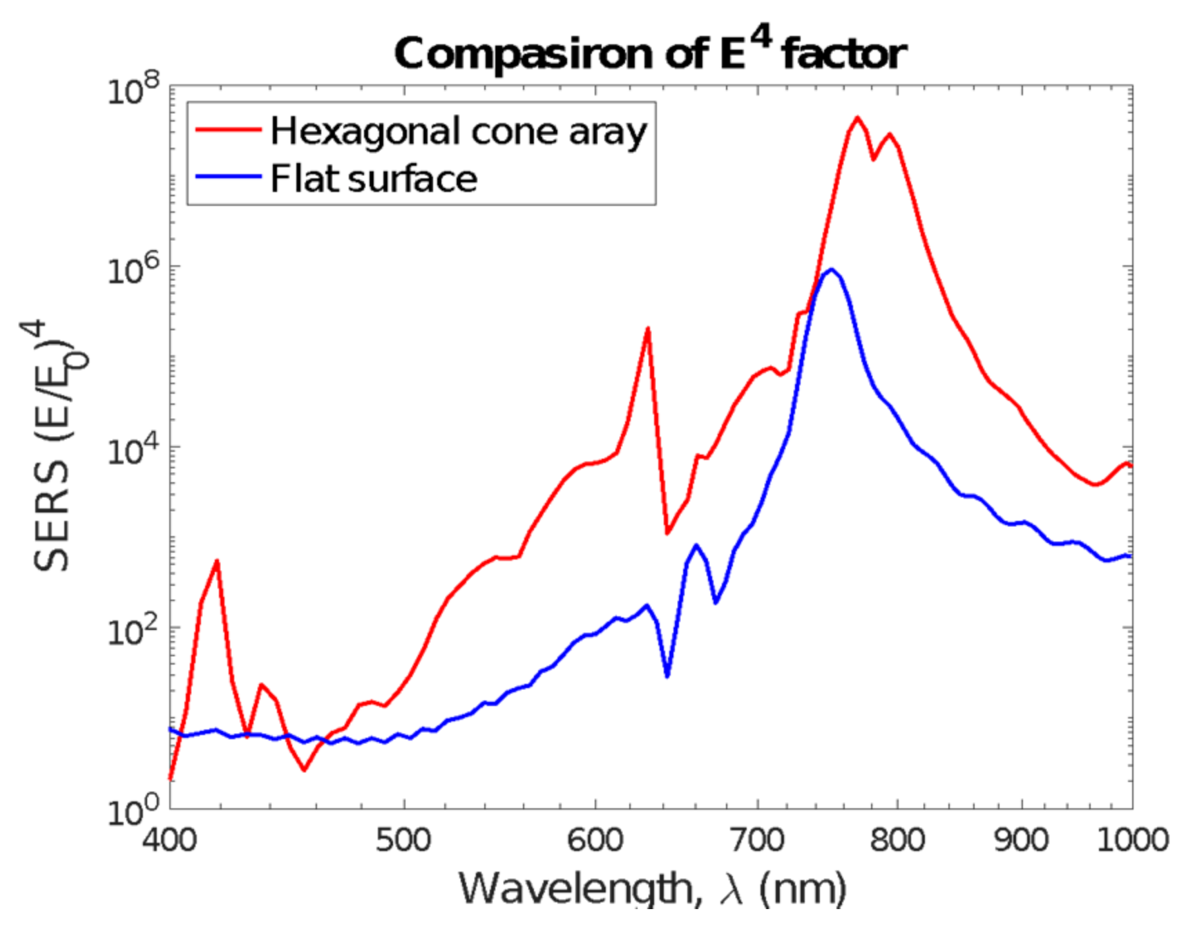
3.1. Nanocone Design and Material Selection for High Field Enhancemnt

A 15 nm reflective film is coated on the surface of the PDMS nano-cone, while leaving the top of the cone uncoated. Gold nanorod with 15 nm in diameter, 45 nm in length is used in our simulation, as was previously reported [14]. Si and gold are considered as the reflective film material coated over the PDMS cone, which would have a large enough refractive index difference from that of the PDMS, reflecting most of the incident light to reach the top of the cone and excite nanorods. Our design would have a plane wave light enter the bottom of the PDMS substrate as shown in Figure 1b. The incident light’s electric field is then funneled into the cavity and excite the nanorod at the top, resulting LSPR around the nanorod. To elucidate the role of the cavity’s photon funneling effect in enhancing a nanorod’s LSPR, the case with one nanorod at the top of the inverse cavity is simulated to get the distribution of electromagnetic fields in cross sections of structures along the axis of the nanorods. In order to see the effect of photon funneling of our design, a flat PDMS surface with gold nanorods on top with at least 840nm separation among them was also simulated. The flat PDMS surface case represents the current common Raman substrates with gold nanorods sprinkled over.
To induce cavity resonance for photon funneling, a high internal reflection inside the cavity is required. According to Fresnel’s equations, a high reflection occurs when the difference of refractive indices of two interface materials is large [24]. Both Si and Au are considered to serve as a coating film for high interreflection, considering the refractive index of PDMS in the visible region is around 1.4, Au with index around 0.3 and Si with index around 4.0. But due to the metallic dissipative nature of Au, the optical loss of Au-coated cavities can be much higher. The power dissipating profile of Si and Au deposited cavities are simulated as shown in Figure 2a,b, across the cross section of the cavity. The power dissipation can be defined as [25], which is directly correlated with the light energy density [26]:
w ( x , z ) = 1 2 ε 0 ω ε ( x , z ) E ( x , z ) 2
In Figure 2a,b, photonic energy is mostly dissipated at the film interface for both Si and Au coated cases. But the intensity in the Au-coated film is nearly 750 times larger than that with the Si film coated case. Figure 2c,d show the electric field intensity with a nanorod at the top. In Figure 2c, with a Si coating, the electric field is enhanced by two orders around the top of the cavity. With gradually narrowing cavity upward and low optical loss at the wall interface, the incident photons are concentrated and delivered to the nanorod at the top of the structure. In Figure 2d, when the electric field is enhanced at the side wall of the cavity, the photons are dissipated and scattered at the cavity wall, before arriving the top. Even though photons are concentrated at a similar level in both cases, the dissipation effect at the gold film makes a huge difference.
Figure 3a,b show the electric field distribution inside of Si- or Au-coated cones with nanorods at the top: the contours indicate the electric field enhancement, and the green arrows in the cavity show the electric vectors. Note that the top of the cone is free of coating to have concentrated photons will not be reflected and reach nanorods. As shown in Figure 1c, the electric field is highly confined around the nanorod at the top of the cone, forming plasmonic hot spots. Inside the cone, the electric vectors exhibit multi-reflection resonance patterns which show the cavity resonance mode. In Figure 3b, the electric field is also highly confined around the nanorod, but the peak intensities are much lower than the case in Figure 3a, indicating that Si film coated cavity design has 5 times higher electric field enhancement than the Au-coated cavity design has. Figure 3c shows the field enhancement performance comparison as a function of exciting light’s wavelength at the top observing plane for Si-coated cone, Au-coated cone and flat surface cases. For this calculation, we segmented the domain into rectangular meshes to use FTDT method reported previously [27,28,29,30]. Each mesh has its own optical property can represent the structure and the surrounding environment. A plane of mesh is chosen as the source plane where the plane wave light is generated numerically. In this plane, we set the magnitude of input electrical vector as E0. In the area close to the Au nanorod, we have chosen a group of meshes to record the optical vector data. From these meshes we can obtain the averaged electrical field intensity E as a function of wavelength and mesh number. We then select the maximum intensity among them and the mesh with the maximum electrical intensity at a given wavelength. We then plot this maximum intensity at different wavelengths as shown in Figure 3c. The simulation result shows that the Raman enhancement at 758 nm can reach up to 108 for the Si-coated case, 106 for the flat surface case and 103 for the Au-coated case. With the help of low-loss photon-concentrating Si-coating, Raman sensitivity of the nanorods on nanocone can be improved over the nanorods on flat surface by 102. The loss at the Au film greatly reduces the electric field of the incident light, resulting field enhancement much lower than that of the nanorods with the flat surface.

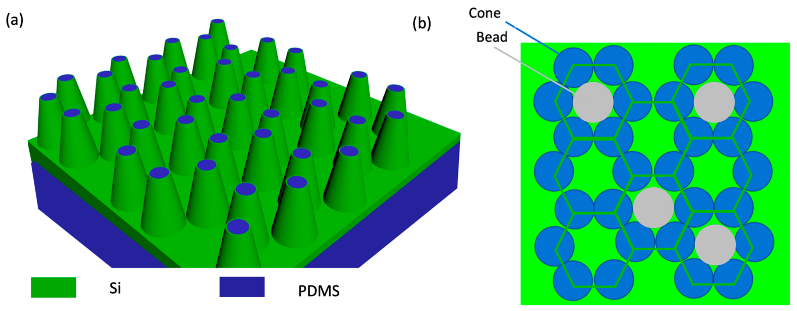
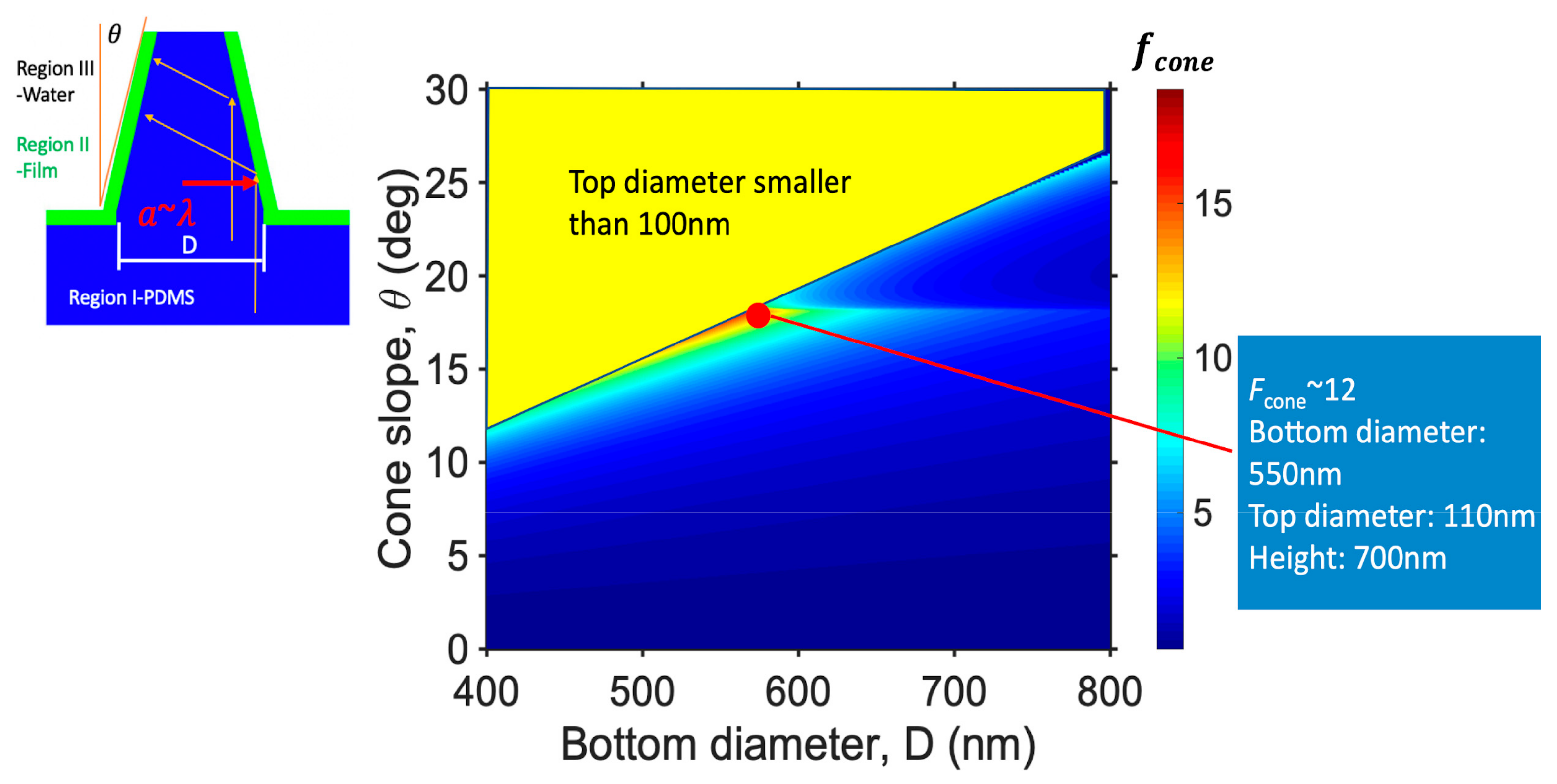
3.2. Nanocone Array Geometry Optimization for Tight Target Cell-Hot Spot Contact

By optimizing the nanocone coating material selection via electric field intensity simulation, the nanorods with Si coated cavity wall can have an enhanced Raman sensitivity by a factor of two over that of the nanorods on flat PDMS substrate. Now it is the key to bring the target cell in a very close proximity to the extremely small hot spots near nanorods. This can be achieved by pulling the magnetic beads toward the cone array in between the cones by applying magnetic field from the bottom. As a result, a cell with 5–6 magnetic beads bonded will be pulled down to the cone array. To have a tight contact between the cone arrays and bacterial cell wall, the cone’s height needs to be taller than the magnetic bead diameter which is usually in the size ~500 nm [20], but not too tall which may exert to much force to break the bead-cell connection while being pulled down. We don’t expect the PDMS cone array will not collapse by this pulling force. The cell wall fluctuates (with possible wrinkles) in the order of ~50 nm, where the dynamic biochemical reaction drives the cell wall to move up and down [26]. The height is chosen as 700 nm to leave 200 nm indentation of cone into the cell wall. From the literature [31] one can see that bacterial cell walls can typically tolerate 200 nm indentation without cell wall ruptures. This 200 nm indentation is bigger than the wall fluctuation as well as to make a stable contact, while avoiding the breakage of the cell wall. In order to increase the number of cones in touch with a single cell, the cone array packing density needs to be maximized, thereby the cone array is arranged into a dense hexagonal pattern in our design as shown in Figure 4a. In order to accept magnetic beads between cones when pulled down, the center of every honeycomb cell is left open as shown in Figure 4b.
The second step is to find the optimal slope and bottom diameter of cones. The relative intensity I r e l a t i v e has the relationship [11]:
I r e l a t i v e E F t o p × N m o l e c u l e
N m o l e c u l e is the number of molecules at the top of the cone and is proportional to the top surface area S t o p . The enhancement at the top of cone E F t o p is positively related to the slope of the cone while S t o p is negatively related. To find the trade-off between E F t o p and S t o p , a function is defined as:
f c o n e = E F t o p × S t o p S i
where S i is the total area, a single cone takes up, on average. This function is actually the ratio between the signal intensity of the cone array to that of the flat surface at the same nanorod deposition density. For a flat surface, fcone is 1, and there is no funneling effect. The effort is to maximize fcone.
The E F t o p is calculated through:
E F t o p = S t o p + π D 2 S t o p × R _ 0.5 π θ S t o p
R _ is the polarization averaged reflection of the film, obtained from Fresnel’s equations. In the calculation, given that the film thickness is 15 nm, much smaller than the wavelength in the film, a thin film approximation is introduced where wavevectors in PDMS and water are close to free space and the wavevector in film is nearly independent of radius a [32]. In the calculation, only the first order of reflection at the surface of the film is taken into account.
In Figure 5, knowing that the top diameter cannot be smaller than 100 nm, we can find an optimal geometry for the cone as bottom diameter 550 nm, top diameter 110 nm and height 700 nm. By using those parameters, the FDTD simulation is performed. Figure 6a shows the field distribution of the cone array. As can be seen here, the photons are funneled and localized near the opening at the top of a cone, where electric field intensity is significantly increased. When placing a nanorod on the top of every cone, it can be seen from Figure 6b that the electric field is highly enhanced around the nanorod with a maximum intensity increase of 80.
The comparison between the hexagonally dense packed cone array and the flat surface regarding the E4 factor is shown in Figure 7. As one can see, the E4 of the nanorod on top of the cone array has reached 108. The improvement that we target is the ratio between the Raman intensity generated by the cone array and the flat commercial substrate, which is 107. This calculation is with the assumptions that 2 substrates have the same nanorod deposition density, the same number of beads are attached to bacteria, and both have the same wavelength which is 758 nm. In summary, this design is supposed to have one order of magnitude improvement at least.

4. Discussion and Conclusions

A novel SERS substrate design is proposed for rapid, culture-free diagnosis of bacterial sepsis. At the present time, SERS sensors have two ways to make contact with the target SERS substrate—by providing colloidal nano particles which adhere to the targets or flat SERS surface on which targets are expected to sit. Both methods have limitations to get right sensitivity unless a high enough number of target cells is available. In the colloidal method, plasmonic nano particles bind with target bacteria in solution which can be heavily affected by the zeta potential and other test conditions. The flat surface approach is to have a nanostructured metal layer on the substrate to be covered with target cells. They both have the following issues and limitations to be improved by our design.
Firstly, loose contact between plasmonic metal and target bacteria is degrading the sensitivity. The Raman signal enhancement by plasmonic metal nanostructures happens when the plasmonic hot spots and the target pathogen come to a very short distance, typically less than 10 nm. There is no long-distance force that can let plasmonic metal and cell wall touch in close contact and generate enhanced signal, resulting the arrival of cells to plasmonic structures is limited by slow diffusion. Our design suggests binding of pathogenic cells to magnetic nanoparticles, and then using a magnetic field to attract magnetic particles down to the 3D metal nanostructures, forcing the target cells to get very close proximity to the hot spots formed on the top of nano-cones instantaneously. Secondly, the incident light cannot illuminate the plasmonic metal under the target cells at the maximum strength. In colloidal method, target bacteria and nano metal particles are randomly bound to each other, and incident light can be blocked by the target cells quite often if they are behind the target cells. For flat surface approach, bacteria would sit at the top of plasmonic surface, and incident light will come from top and large portion of incident light will be blocked/ absorbed by the target bacteria, and small number of photons can reach the plasmonic metal at the maximum strength. Our design allows light comes from the bottom through the transparent nanostructures, thereby has no photon blocking problem. Thirdly, the limited light field enhancement of the current colloidal and flat surface approach which lingers around 106 can be improved by the transparent nanocones where the radius decreases along the light path. A high reflective and low loss layer is deposited outer surface of the cone. When this higher concentration of “photon gas” reaches the plasmonic metal nanorod at the top of the cone array, the Raman signal enhancement can be as high as 108. The high sensitivity originates from the combination of photon funneling, dense packing, and optimized cone shape to ensure the close contact of the target to the hot spots. The Raman enhancement factor can be increased by two orders of magnitude while only reducing the contact area by one order and makes overall sensitivity to be one order higher compared with the conventional flat nanosurface approach. The Si-coated inverted cone structure proposed in this paper has the advantages of low-cost and large-scale production, and it is easy to incorporate an immunomagnetic pathogen collecting workflow.
The proposed design can use existing Raman configuration with the incident light entering the substrate from the bottom, funneling through the transparent PDMS medium which has a conical shape. The same backscattering configuration of the existing Raman instrument can be used by switching the incident light from top to bottom. This design is similar to the TERS (Tip Enhanced Raman Spectroscopy) system which has one tip with very high electric field hot spot. But from the point of sample-substrate interface, this design is close to SERS configuration since samples can be placed on the substrate without precise positioning of them. Conventional SERS have nanoscale-roughened metal tips randomly formed at the substrate surface while our design has deterministically located nanocones with one or multiple gold nanorods at the top of each cone of the array. The SERS substrate proposed in this report can be used to detect sepsis and other pathogens from body fluids like fungal cells with higher sensitivity than conventional SERS provides. This work will facilitate the development of a novel optical nano-bio-substrate for fast and convenient pathogen diagnosis.

Author Contributions

Conceptualization, S.-G.K.; methodology, Z.J. and S.-G.K.; software, Z.J.; validation, Z.J. and S.-G.K.; formal analysis, Z.J.; investigation, Z.J., S.A. and W.A.; writing—original draft preparation, Z.J. and S.-G.K.; writing—review and editing, S.-G.K.; visualization, Z.J.; supervision, S.-G.K., E.A.-S. and A.E.; All authors have read and agreed to the published version of the manuscript.

Funding

This research was supported by the funding from the Institute for Research and Medical Consultations (IRMC) at Imam Abdulrahman Bin Faisal University (IAU), under an agreement between IAU/IRMC and MIT.

Institutional Review Board Statement

Not applicable.

Informed Consent Statement

Not applicable.

Data Availability Statement

The data presented in this study are available on request.

Acknowledgments

This work was supported by funding from the Institute for Research and Medical Consultations (IRMC) at Imam Abdulrahman Bin Faisal University (IAU), Saudi Arabia, under an agreement between IAU/IRMC and MIT.

Conflicts of Interest

The authors declare no conflict of interest.

References

  1. Angus, D.C.; van der Poll, T. Severe sepsis and septic shock. N. Engl. J. Med. 2013, 369, 840–851. [Google Scholar] [CrossRef]
  2. Jawad, I.; Lukšić, I.; Rafnsson, S.B. Assessing available information on the burden of sepsis: Global estimates of incidence, prevalence and mortality. J. Glob. Health 2012, 2, 10404. [Google Scholar] [CrossRef]
  3. Mancini, N.; Carletti, S.; Ghidoli, N.; Cichero, P.; Burioni, R.; Clementi, M. The Era of Molecular and Other Non-Culture-Based Methods in Diagnosis of Sepsis. Clin. Microbiol. Rev. 2010, 23, 235–251. [Google Scholar] [CrossRef] [Green Version]
  4. Kirpalani, H.; Huang, L.; Michenko, M.J.; Duffet, M. Manual of Pediatric Intensive Care. PMPH-USA. 2009. Available online: https://www.wolterskluwer.com/en/solutions/ovid/manual-of-pediatric-intensive-care-8132 (accessed on 25 August 2021).
  5. Assad, O.N.; Gilboa, T.; Spitzberg, J.; Juhasz, M.; Weinhold, E.; Meller, A. Light-enhancing plasmonic-nanopore biosubstrate for superior single-molecule detection. Adv. Mater. 2017, 29, 1605442. [Google Scholar] [CrossRef]
  6. Yanik, A.A.; Cetin, A.E.; Huang, M.; Artar, A.; Mousavi, S.H.; Khanikaev, A.; Connor, J.; Shvets, G.; Altug, H. Seeing protein monolayers with naked eye through plasmonic Fano resonances. Proc. Natl. Acad. Sci. USA 2011, 108, 11784–11789. [Google Scholar] [CrossRef] [Green Version]
  7. Lee, K.L.; Huang, J.B.; Chang, J.W.; Wu, S.H.; Wei, P.K. Ultrasensitive biosubstrates using enhanced fano resonances in capped gold nanoslit arrays. Sci. Rep. 2015, 5, 8547. [Google Scholar] [CrossRef] [PubMed] [Green Version]
  8. Chen, C.K.; Li, C.T.; Yen, T.J.; Lai, Y.C.; Chang, Y.T. A multi-functional plasmonic biosubstrate. Opt. Express 2010, 18, 9561–9569. [Google Scholar]
  9. Kim, K.; Yoon, J.K. Raman Scattering of 4-Aminobenzenethiol Sandwiched between Ag/Au Nanoparticle and Macroscopically Smooth Au Substrate. J. Phys. Chem. B 2005, 109, 20731–20736. [Google Scholar] [CrossRef] [PubMed]
  10. Xu, W.; Ling, X.; Xiao, J.; Dresselhaus, M.S.; Kong, J.; Xu, H.; Liu, Z.; Zhang, J. Surface enhanced Raman spectroscopy on a flat graphene surface. Proc. Natl. Acad. Sci. USA 2012, 109, 9281–9286. [Google Scholar] [CrossRef] [Green Version]
  11. Tao, A.R.; Yang, P. Polarized Surface-Enhanced Raman Spectroscopy on Coupled Metallic Nanowires. J. Phys. Chem. B 2005, 109, 15687–15690. [Google Scholar] [CrossRef] [PubMed]
  12. Shen, H.X.; Zou, W.J.; Yang, Z.L.; Yuan, Y.X.; Xu, M.M.; Yao, J.L.; Gu, R.A. Surface-enhanced Raman spectroscopy on single Fe2O3@Au spindle nanoparticle: Polarization dependence and FDTD simulation. J. Opt. 2015, 17, 114014. [Google Scholar] [CrossRef]
  13. Puttaswamy, S.; Lee, B.D.; Sengupta, S. Novel Electrical Method for Early Detection of Viable Bacteria in Blood Cultures. J. Clin. Microbiol. 2011, 49, 2286–2289. [Google Scholar] [CrossRef] [Green Version]
  14. Premasiri, W.R.; Sauer-Budge, A.F.; Lee, J.C.; Klapperich, C.M.; Ziegler, L.D. Rapid bacterial diagnostics via surface enhanced Raman microscopy. Spectroscopy 2012, 27, s8-31. [Google Scholar]
  15. Yue, W.; Wang, Z.; Whittaker, J.; Lopez-Royo, F.; Yang, Y.; Zayats, A.V. Amplification of surface-enhanced Raman scattering due to substrate-mediated localized surface plasmons in gold nanodimers. J. Mater. Chem. C 2017, 5, 4075–4084. [Google Scholar] [CrossRef] [Green Version]
  16. Shioi, M.; Jans, H.; Lodewijks, K.; Van Dorpe, P.; Lagae, L.; Kawamura, T. Tuning the interaction between propagating and localized surface plasmons for surface enhanced Raman scattering in water for biomedical and environmental applications. Appl. Phys. Lett. 2014, 104, 243102. [Google Scholar] [CrossRef]
  17. Shan, D.; Huang, L.; Li, X.; Zhang, W.; Wang, J.; Cheng, L.; Feng, X.; Liu, Y.; Zhu, J.; Zhang, Y. Surface Plasmon Resonance and Interference Coenhanced SERS Substrate of AAO/Al-Based Ag Nanostructure Arrays. J. Phys. Chem. C 2014, 118, 23930–23936. [Google Scholar] [CrossRef]
  18. Paniel, N.; Baudart, J. Colorimetric and electrochemical genosensors for the detection of Escherichia coli DNA without amplification in seawater. Talanta 2013, 115, 133–142. [Google Scholar] [CrossRef]
  19. Wang, J.; Wu, X.; Wang, C.; Shao, N.; Dong, P.; Xiao, R.; Wang, S. Magnetically Assisted Surface-Enhanced Raman Spectroscopy for the Detection of Staphylococcus aureus Based on Aptamer Recognition. ACS Appl. Mater. Interfaces 2015, 7, 20919–20929. [Google Scholar] [CrossRef]
  20. Sha, M.; Xu, H.; Natan, M.J.; Cromer, R. Surface-Enhanced Raman Scattering Tags for Rapid and Homogeneous Detection of Circulating Tumor Cells in the Presence of Human Whole Blood. J. Am. Chem. Soc. 2008, 130, 17214–17215. [Google Scholar] [CrossRef] [Green Version]
  21. Lesaicherre, M.L.; Paxon, T.L.; Mondello, F.J.; Burrell, M.C.; Linsebigler, A. Portable Raman instrument for rapid biological agent detection and identification. SPIE Def. Secur. Sens. 2009, 7319, 73190C. [Google Scholar] [CrossRef]
  22. Chou, J.B.; Yeng, Y.X.; Lee, Y.E.; Lenert, A.; Rinnerbauer, V.; Celanovic, I.; Soljačić, M.; Fang, N.X.; Wang, E.N.; Kim, S.-G. Enabling Ideal Selective Solar Absorption with 2D Metallic Dielectric Photonic Crystals. Adv. Mater. 2014, 26, 8041–8045. [Google Scholar] [CrossRef] [PubMed] [Green Version]
  23. Palik, E.D. Handbook of Optical Constants of Solids (Volume 3); Academic Press: Cambridge, MA, USA, 1998. [Google Scholar]
  24. Zhang, Z.M. Nano/Microscale Heat Transfer; Springer: Berlin/Heidelberg, Germany, 2020. [Google Scholar]
  25. Zhao, B.; Zhao, J.M.; Zhang, Z.M. Enhancement of near-infrared absorption in graphene with metal gratings. Appl. Phys. Lett. 2014, 105, 031905. [Google Scholar] [CrossRef]
  26. Hosseini, P.; Abidi, S.Z.; Du, E.; Papageorgiou, D.P.; Choi, Y.; Park, Y.; Higgins, J.M.; Kato, G.; Suresh, S.; Dao, M.; et al. Cellular normoxic biophysical markers of hydroxyurea treatment in sickle cell disease. Proc. Natl. Acad. Sci. USA 2016, 113, 9527–9532. [Google Scholar] [CrossRef] [PubMed] [Green Version]
  27. Grimault, A.-S.; Vial, A.; De La Chapelle, M.L. Modeling of regular gold nanostructures arrays for SERS applications using a 3D FDTD method. Appl. Phys. A 2006, 84, 111–115. [Google Scholar] [CrossRef]
  28. Tira, C.; Daniela, T.; Timea, S.; Simion, A. Finite-difference time-domain (FDTD) design of gold nanoparticle chains with specific surface plasmon resonance. J. Mol. Struct. 2014, 1072, 137–143. [Google Scholar] [CrossRef]
  29. Vial, A.; Laroche, T. Description of dispersion properties of metals by means of the critical points model and application to the study of resonant structures using the FDTD method. J. Phys. D Appl. Phys. 2007, 40, 7152–7158. [Google Scholar] [CrossRef]
  30. Wang, T.; Zhang, Z.; Liao, F.; Cai, Q.; Li, Y.; Lee, S.; Shao, M. The effect of dielectric constants on noble metal/semiconductor SERS enhancement: FDTD simulation and experiment validation of Ag/Ge and Ag/Si substrates. Sci. Rep. 2014, 4, 1–8. [Google Scholar] [CrossRef] [PubMed] [Green Version]
  31. Abu-Lail, N.I.; Camesano, T.A. The effect of solvent polarity on the molecular surface properties and adhesion of Escherichia coli. Colloids Surf. B Biointerfaces 2006, 51, 62–70. [Google Scholar] [CrossRef]
  32. Lee, C.S.; Lee, S.-W.; Chuang, S.-L. Normal Modes in an Overmoded Circular Waveguide Coated with Lossy Material. IEEE Trans. Microw. Theory Tech. 1986, 34, 773–785. [Google Scholar] [CrossRef] [Green Version]
Figure 1. The illustration of nanocone structure designed; (a) gold nanorod(s) are located at the top of the transparent PDMS (Polydimethylsiloxane) cones coated with thin Si, (b) Internal reflection of incident light from the bottom reaches nanorods, (c) Simulations shows electric field enhancement at the tips of the nanorod (one nanorod case).
Applsci 11 08067 g001
Figure 2. 758 nm power dissipation distribution for cross sections of (a) Si-coated (b) Au-coated cones without nanorod. 758 nm electric distribution for cross sections of (c) Si-coated (d) Au-coated cones without nanorod.
Applsci 11 08067 g002
Figure 3. 758 nm electric field in cross sections of (a) Si coated (b) Au coated inverse cavity without nanorod (c) Electric filed enhancement spectrum comparison for 3 structures (Si-coated nanocone with one top nanorod, Au-coated nanocone, Nanorod on flat PDMS) (d) Illustration of the nanocone cross section with one nanorod.
Applsci 11 08067 g003
Figure 4. Nanocone array structure (a) Illustration of honeycomb-cone array structure. (b) Illustration of vacant cell center in order to locate the magnetic beads.
Applsci 11 08067 g004
Figure 5. fcone as a function of bottom diameter and slope.
Applsci 11 08067 g005
Figure 6. 758 nm electric field distribution at the top of cone array (a) without and (b) with nanorod.
Applsci 11 08067 g006
Figure 7. The comparison of E4 factor between hexagonal dense packing cone array and flat surface.
Applsci 11 08067 g007
Publisher’s Note: MDPI stays neutral with regard to jurisdictional claims in published maps and institutional affiliations.

