Abstract
The helical resonator is a scheme for the production of high voltage at radio frequency, useful for gas breakdown and plasma sustainment, which, through a proper design, enables avoiding the use of a matching network. In this work, we consider the treatment of the helical resonator, including a grounded shield, as a transmission line with a shorted end and an open one, the latter possibly connected to a capacitive load. The input voltage is applied to a tap point located near the shorted end. After deriving an expression for the velocity factor of the perturbations propagating along the line, and in the special case of the shield at infinity also of the characteristic impedance, we calculate the input impedance and the voltage amplification factor of the resonator as a function of the wave number. Focusing on the resonance condition, which maximizes the voltage amplification, we then discuss the effect of the tap point position, dissipation and the optional capacitive load, in terms of resonator performance and matching to the power supply.
1. Introduction
The generation in the laboratory of an ionized gas, also called plasma, requires, in most instances, application to the originally neutral gas of an electric field that is large enough to start an avalanche process of ionization events driven by free electrons (also called breakdown). While the required conditions greatly vary, depending on many variables related to the chosen experimental layout and working conditions, in broad terms, the typical applied voltages are in the range of a few hundreds volts to several kV. Furthermore, the voltage can be stationary or varying in time with different rates: the rate determines both the technology to be used to generate and transmit the required voltage and the physics of the breakdown process and of the produced plasma. Among the different possibilities, the radio frequency (RF) voltage is a possible choice. This term broadly represents voltages varying with a frequency ranging from around 1 MHz to several hundred MHz. RF plasmas are characterized by a lower voltage required for breakdown with respect to lower frequency devices, and by the possibility of avoiding contact between electrodes and plasma, especially when the inductive coupling regime is achieved.
In general terms, the production of a RF plasma requires a generator (possibly composed of an oscillator and an amplifier), and a matching network, which in this case, has the double role of matching the device input impedance to the output impedance of the generator, and to magnify the voltage to the required value for breakdown and subsequent plasma sustainment. The impedance matching feature is necessary to minimize the power reflected from the load to the generator. This is not an issue at lower frequencies, where the wavelength of the voltage disturbance is much larger than the apparatus size, so that instantaneous propagation can be assumed, and lumped element circuit treatments are appropriate. It becomes, however, important in the MHz range and beyond, where the wavelength becomes comparable to the system size. In this case, a finite time is required for voltage variation propagation, and transmission line theory comes into play. It is worth noting that this brings many similarities between the field of plasma technology and that of radio transmission, although in the latter, voltage amplification is not a requirement, but rather an issue that should eventually be taken into account to avoid undesirable breakdown of air.
Many possibilities exist for matching network construction, and sophisticated solutions are now commercially available. There is, however, a solution that has already been used for plasma generation, but has not encountered great diffusion despite its potential simplicity: the helical resonator. The helical resonator, as will be described in more detail in the following, is an open-ended air core coil that can be used both for voltage amplification, exploiting a resonance condition, and for impedance matching, by proper design of its layout. The absence of a ferrite core implies that very low dissipation levels are attainable if proper care is put in the design of the device, allowing the use of relatively low-power generators.
It is worth making here the historical annotation that there is a strong connection between the helical resonator and the “extra coil” used by Nikola Tesla in his work at Colorado Springs to produce high voltage at high frequency [1]. Indeed, Tesla evolved from using a loosely coupled resonant transformer to a tightly coupled one, with the secondary circuit connected to an “extra coil”, which was a capacitively loaded helical resonator. Keeping in mind that Tesla used frequencies of tens of kHz, so several issues related to dissipation are substantially different in our case (and the apparatus size as well), it is, however, important to remark that our present discussion is also useful for a better understanding of his work and of the modern day Tesla coil working principle.
Despite being a concept developed at the end of the XIX century, the literature on the helical resonator working principle is somehow scattered and also includes empirical formulas not derived from first principles [2]. This is also due to the fact that the same topic has been studied from several angles. Indeed, the concept is interesting for the following fields:
- Plasma generation [3,4,5,6];
- Ion trap antennas [7];
- Self-capacitance of coils [8,9];
- RF filters [10,11];
- Tesla coil construction [12];
- Precision measurements and metamaterial research [13,14,15,16,17].
In each of these fields, different authors treated the problem with different taste and emphasis on some issues, and collecting all these contributions in a unified view has proven to be not trivial. We thus would like to give a summary of the most important results on this subject, in the hope that this can prove useful to future scientists and practitioners who wish to properly understand this concept. In particular, we derive formulas that allow to predict the performance of a resonator from its basic properties, and illustrate a possible use for designing resonators, satisfying the given requirements. The whole discussion surrounds the resonator without plasma: the effects of a plasma formed inside the device will be the object of a forthcoming publication.
The paper is organized as follows: in Section 2, we introduce the geometry of the device we wish to describe, and the different flavors that it can take; in Section 3, we describe the propagation of electromagnetic perturbations in the resonator, deriving the main characteristics of the device, which are characteristic impedance and the velocity factor, as a function of its geometry. Armed with these results, we then move to Section 4 to model the resonator as a transmission line, looking for the resonance condition, which is the frequency that maximizes the voltage amplification at the open end, and for the input impedance, which should be adapted so as to match the output impedance of the generator. In Section 5, the special case of a resonator with the shield immediately near the helical conductor is treated, as this is both the most promising for plasma production and also the one that allows a fully analytical treatment. In Section 6, the effect of a capacitive load connected to the resonator (including parasitic capacitance) is discussed. The results found up to this point are then checked against the experimental data in Section 7. Finally, in Section 8, the conclusions are drawn.
2. Geometry
The basic geometry of a helical resonator, as defined in the context of this paper, is shown in Figure 1. The resonator consists of a helically wound conductor of length L, with one end (which we shall call bottom end in the following) grounded, while the other (top end) is left open, or connected to a load. We indicate with b the helix radius, with H its height, and with N the number of turns. The helix pitch is given by the following:
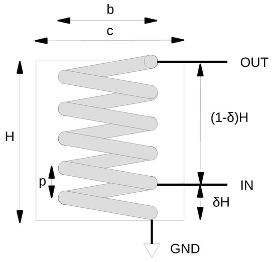
Figure 1.
Schematics of the helical resonator. The terminals labeled IN and OUT are the ones where the voltages and are evaluated. The external rectangle represents the screen.
The driving voltage, labeled , is fed in an intermediate point, named “tap point”, usually near the bottom end. The tap point axial position, normalized to H, is labeled as . The resonator is covered by a grounded conducting shield, of radius c. This shield, not present in all treatments (if absent, it may be considered at infinity) represents the second conductor of the transmission line for which the helix is the first one, according to the modeling presented in Section 4. The voltage at the top end of the resonator is labeled .
It is useful to emphasize that the shieldless resonator is fully defined by the three parameters , while in the more general case where the shield is present, the fourth parameter c is required. In principle, also the thickness of the helical conductor should be taken into account: however, this has only an effect on the dissipation due to the skin effect, and this effect is not so important at RF since the skin thickness is much smaller than any practical conductor thickness, so that the current is anyway flowing on the conductor surface. Therefore, we shall not consider this further parameter in our model, although one should be aware that p cannot be smaller than twice such thickness, and this puts a lower bound on the angle defined below.
It is worthwhile to introduce the pitch angle , defined as the following:
This will typically be quite small, expressing the fact that the helix is tightly wound, for the reason of compactness of the device; however, nothing prevents making it large, if required. The total length of the helical conductor can be expressed in terms of the other parameters as
In most practical situations, , so that .
It is also useful to introduce the aspect ratio, defined as . This quantity gives an immediate idea of how elongated the coil is. In the following, we actually use, for convenience of notation, the inverse aspect ratio:
It is useful for the following to notice that .
3. Propagation of Electromagnetic Perturbations into the Resonator
In order to properly model the helical resonator, we first need to understand how electromagnetic disturbances propagate in it, deriving a dispersion relation that is useful for obtaining the basic properties, such as phase velocity and, in a limit case, the characteristic impedance of the resonator seen as a transmission line. To accomplish this task, it is customary to model the resonator as a “sheath helix”. This name is used to indicate an idealized anisotropically conducting cylindrical surface of infinite length, with infinite conductivity along the helix and zero conductivity normal to it. This model is possibly originally due to Ollendorf [18], and was treated by Sichak [19] and by Sensiper [20].
The starting point are Maxwell equations in vacuum as follows:
Combining them, we obtain the wave equation as follows:
where is the speed of light, which has as solutions in free space the electromagnetic plane waves.
We now consider the cylindrical geometry of the resonator and seek solutions of the form . Here, is the axial wavevector, and m the azimuthal mode number. Furthermore, we restrict ourselves to modes, because higher order modes are relevant only at very high frequencies. We thus deal with azimuthally symmetric perturbations of the form . The wave equation becomes the Helmholtz equation as follows:
Introducing (this is the wavevector of electromagnetic plane waves in vacuum), and defining the radial eigenvalue,
we have the following:
The general solution of this equation is of the form , where and are the modified Bessel functions of the first and second kind, respectively. It is important to remark, in order to avoid confusion, that k is here used as a normalized version of the frequency, whereas is the actual wavenumber of the perturbations, and defines the radial oscillation of the electromagnetic field perturbation. Normally, , so that .
Let us now label with 1 the region inside the coil () and with 2, the region between the coil and the shield (). Taking into account that diverges in , we have the following physically admissible solutions for the axial field components:
The other components of the fields are deduced from Maxwell equations as follows:
We now apply the boundary conditions relevant for the sheath helix. On the helix surface () the longitudinal electric field has to be zero, due to the hypothesis of infinite conductivity. This gives the following:
The transverse component must be continuous, and since this is the only component present, this gives the following:
which makes redundant one of the two previous ones. The longitudinal component of the magnetic field must be continuous since there is no current flowing on the surface perpendicular to this direction, so that the following holds:
Finally, on the conducting shield () the electric field will be zero, that is,
which complete the set of six conditions required to fix the six constants , , , , , .
After some algebra, the following eigenvalue equation for is obtained:
This is the result that was obtained by Uhm and Choe [21], and also by Anicin [22], which is incorrectly reported (likely due to a mere transcription error) in Equation (25) of Niazi et al. [23]. It has the form , which means that once the normalized frequency and the geometric factors and are specified, can be obtained, and subsequently, the normalized wave number using expression (9). The function is plotted in Figure 2 for different values of . It can be seen that for large values of , this is a strongly decreasing function of , whereas it tends to the constant value of 1 when the screen goes very near the coil. All the curves group together onto the unit value for large (indicatively, larger than 1). In Figure 2 are also reported the eigenvalues obtained from Equation (24), as a function of the parameter . The curves display an increasing behavior of the eigenvalue with the frequency, and converge to the relation as the shield approaches the coil.
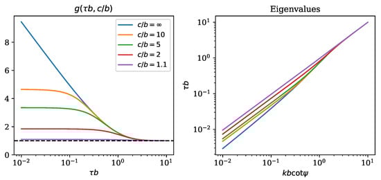
Figure 2.
Left: function entering the eigenvalue equation, plotted as versus for different values of . Right: solutions of the eigenvalue equation, plotted versus for different values of .
Once the eigenvalue equation is solved, one has the frequency as a function of the wave number, that is, the dispersion relation. It is then possible to evaluate the velocity factor, defined as the phase velocity normalized to :
We should now recall that we are dealing with axial propagation, and therefore the velocity factor refers to the axial velocity. However, this holds in the sheath helix approximation, while in reality, the voltage pulse propagation takes place longitudinally, along the helically shaped conductor. If we consider the longitudinal propagaton along the helical conductor, the wave vector is given, through a simple projection, by . Thus, the longitudinal velocity factor, given that the phase velocity is the ratio of the angular frequency to the wave number, is given by .
Such a longitudinal velocity factor is shown in Figure 3 for two different values of the pitch angle, corresponding to a tightly wound helix () and to a more loosely wound one (). It can be seen that the longitudinal propagation takes place at a speed somehow larger than the speed of light in the vacuum, and that its frequency dependence is almost the same regardless of the pitch angle, with only a shift in the normalized frequency axis. We can identify three regions: at low frequency, the velocity factor is constant, with a value of 1 for the shield on the helix and increases to values larger than 3 when the shield is brought far away; a transition region; and a high frequency region where the propagation speed is equal to , regardless of the shield position. We want to emphasize that the velocity factor is frequency dependent, so the propagation is dispersive.
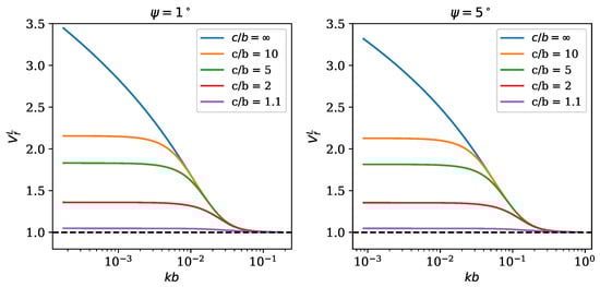
Figure 3.
Longitudinal velocity factor plotted as a function of the normalized frequency , for different values of the shield proximity ; the left panel refers to a pitch angle , the right panel to .
To put things in perspective, we can consider, for example, that for the industrial frequency MHz, the plane wave wavelength is 11 m, so m. For a coil with a diameter of 10 cm, this gives . This can be in the region where all longitudinal velocity factors collapse on a single curve or not, depending on the pitch angle value.
Before concluding this section, it is worth addressing in more detail two limit cases. The first one is the case without the shield, which, in our formulation, corresponds to . It is straightforward to show that in this case, the eigenvalue equation reduces to the following:
This result was quoted by several authors, in the context of analyzing the self-capacitance of a helical coil [24]. The rest of the analysis proceeds as before, but it is worth mentioning that the axial velocity factor can be approximated reasonably well, at least in the transition region, by the following expression [24]:
where is the coil diameter. This is illustrated in Figure 4, which shows a superposition of the exact longitudinal velocity factor obtained from the resolution of the eigenvalue equation superposed to that obtained from the empirical formula above. It can be seen that, as long as the frequency is low enough so that the longitudinal velocity factor is larger than 1, the approximated value is reasonably close to the exact one.
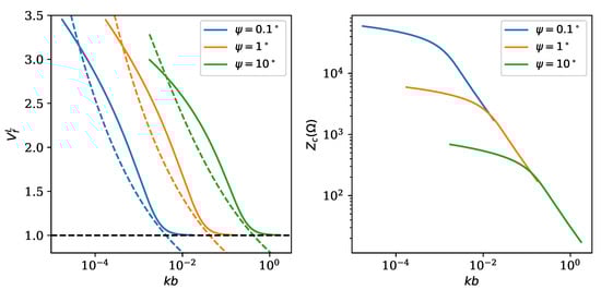
Figure 4.
Left: exact longitudinal velocity factor for the case without shield plotted as a function of the normalized frequency (solid lines) and approximation obtained from Equation (27) (dashed lines), for three different values of the pitch angle . Right: characteristic impedance for the case without shield plotted as a function of the normalized frequency , for three different values of the pitch angle .
For this particular case, an analytic formula for the characteristic impedance of the resonator seen as a transmission line was derived [24]. This is given by the following (expressed in Ohm):
It is worth noting that the product of Bessel functions that appears in this formula is a decreasing function of its argument. The characteristic impedance for the case without shield is also plotted in Figure 4, as a function of the normalized frequency , for different pitch angles. It can be seen that the characteristic impedance decreases with frequency. For high frequencies, the curves all collapse on the following value:
whereas at low frequencies, they fall below this curve. Typical characteristic impedance values for wavelengths much larger than the coil radius fall indicatively in the range of the k for pitch angles between and .
The second limit case is that in which the shield is directly over the coil, that is, . In this case, the eigenvalue equation simply reduces to the following:
so that no numerical resolution is required. The dispersion relation becomes nondispersive.
with a velocity factor , and therefore a longitudinal velocity factor : the voltage pulses propagate along the conductor at the speed of light in vacuum.
We conclude this section by remarking that, in general, both the velocity factor and the characteristic impedance are functions of the frequency of the pitch angle (which is the only coil geometrical parameter entering the treatment) and of the shield proximity .
4. The Helical Resonator as a Transmission Line
Armed with the expressions for the velocity factor and, for the shieldless case, of the characteristic impedance, we are now in the position to model our helical resonator as a transmission line, with the helical coil as one conductor and the shield as the other, and with voltage applied to the tap point. The basic concepts of transmission line modeling are recalled, for the reader’s convenience, in Appendix A. The aim of this model is to obtain expressions for the two quantities, which are to be optimized for plasma generation, that is, the input impedance, which ideally should match the output impedance of the power supply (typically 50 ), and the voltage amplification factor that we want to maximize.
We start from basic Equations (A1) and (A2), describing the spatial behavior of voltage and current for a perturbation at frequency :
where z is a coordinate running along the cylinder axis and , with being the attenuation constant and the wave number of the propagating perturbation. We consider separately the bottom and the top part of the resonator as two different transmission lines, each with its own boundary conditions. The bottom part, being short circuited (), gives the conditions at the grounded end () and the tap point ():
where we have introduced . These yield the following solution:
For the top part, which is open () we have the following:
yielding the following:
The voltage at the line endpoint is , so the following holds:
We shall call “voltage amplification factor” the modulus of this ratio. The total input current at the tap point is the following:
so that the input impedance of the resonator is given by the following:
This is generally complex, with a resistive and a reactive part.
The expressions found for the input impedance and for the amplification factor are functions of the frequency, first because the wave number is related to the frequency through the velocity factor (), and also because the velocity factor and the characteristic impedance are both frequency dependent. The dependence on the frequency of the attenuation coefficient , which also exists, is neglected in the following.
In order to understand the behavior of the expressions found above, we first make the assumption that is independent of frequency, and we plot the relevant quantities as a function of the “electrical length” (which, we remind, is equal to ), expressed in units of . This quantity is related to the frequency through the velocity factor. The results are shown in Figure 5 for three different values of the attenuation factor .
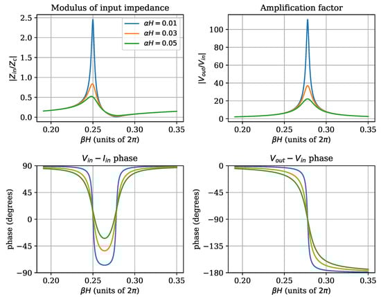
Figure 5.
Behavior of the helical resonator modeled as a transmission line plotted as a function of the normalized wave number expressed in units of , for three different values of the attenuation factor . The curves are computed for . Top left: modulus of the input impedance normalized to the characteristic impedance . Top right: voltage amplification factor . Bottom left: phase shift in degrees between input voltage and input current. Bottom right: phase shift in degrees between the input voltage and the output voltage.
The modulus of the input impedance displays a maximum and a minimum. The maximum is found for an electrical length as follows:
This corresponds to the condition of the entire coil length equal to (either considering the axial direction, with wavelength and length H, or the longitudinal direction, with wavelength and length L). It is worth noting that this point corresponds to a rather large impedance, of the order of the characteristic impedance, and thus in the range of the k.
The voltage amplification factor displays a maximum, corresponding to the minimum of the impedance modulus. By analyzing expression (42), it can be seen that the maxima of the amplification factor occur at the following resonant wave numbers:
which correspond to increasing resonant frequencies. These are resonances computed by taking into account only the length of the top part of the resonator. The peak displayed in the graph, and the only one which will be considered in the following, is . The extension of the results to higher order resonances is straightforward. Other authors have studied resonances of a higher order in the context of plasma production [25]. It is clear how the distance between the two critical points, that is, the point of maximum impedance and the resonance, increases as is increased. The amplification factor at the resonance is the following:
Since in practical cases, , this can be approximated by the following:
This expression elucidates the importance of achieving low dissipation in order to obtain a large voltage amplification.
Looking at the phases, it can be seen that the input voltage and current are in quadrature at low frequencies, then go in phase at the impedance maximum; then the phase is inverted, has another zero at the amplification factor maximum and returns to at high frequencies. Thus, the two critical points, that is, the maximum and minimum of the input impedance modulus, both approximately correspond to a real impedance. It is worth also noting that the extension of the phase reversal region between the two depends on the attenuation factor, so that this can be used as an indirect way of measuring it. Indeed, if the dissipation is too high, the phase will never become negative, and no purely resistive input impedance is possible. Finally, the input and output voltages are in phase at low frequencies, become in quadrature at the amplification factor maximum, as expected from Equation (48), and then go in phase opposition. As is shown in the next section, the distance between the two critical points depends on the parameter . In the following, we are concerned mainly with the point of maximum output voltage, which is related to a resonance of the system, and which represents the optimal condition for plasma generation. The voltage amplification becomes, of course, smaller as the attenuation factor increases, so minimizing dissipation is an important part of the design of an effective resonator.
A similar analysis can be performed by keeping the dissipation constant, and varying the tap point relative position . This is shown in Figure 6. It can be observed that the maximum modulus of impedance increases as is increased, while the amplification factor peak moves to the right, as expected, and grows in magnitude. The same shift occurs to the phase shift between the input and output voltage. The region of negative phase becomes deeper and wider. This last result shows that, for the given resonator parameters, there is a minimum that allows a purely resistive input impedance.
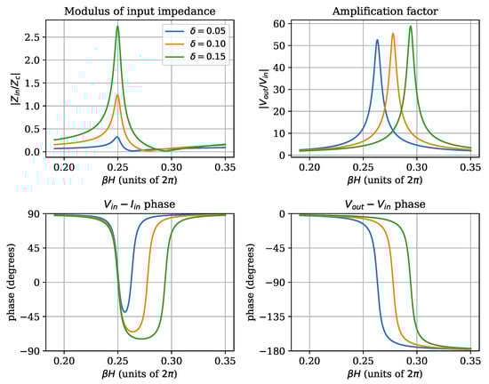
Figure 6.
Behavior of the helical resonator modeled as a transmission line plotted as a function of the normalized wave number expressed in units of , for three different values of the relative tap position . The curves are computed for . Top left: modulus of the input impedance normalized to the characteristic impedance . Top right: voltage amplification factor . Bottom left: phase shift in degrees between input voltage and input current. Bottom right: phase shift in degrees between the input voltage and the output voltage.
Since in the context of plasma production, the interest is focused on the resonance, which gives the maximum voltage amplification, we now plot the resistance at the peak, the resistance at the resonance, their ratio and the voltage amplification factor at the resonance, as a function of the dissipation factor for three values. This is shown in Figure 7. It can be seen that the peak resistance is of the same order of magnitude of the characteristic impedance, that is, of the order of the k, and decreases as the dissipation grows, while it increases when the tap point is moved to the right. On the contrary, the resistance at the resonance, which is the relevant parameter for the operation of the resonator as a voltage amplifier, increases both with dissipation and with tap position. This shows that changing the tap position is a way to achieve an impedance matching of the device with the power supply. Finally, the ratio of the output voltage to the input one is shown, as could be expected from energy considerations and from the previous figures, to decrease with dissipation, with a modest dependence on the tap position in the explored range. In the figure, we have also plotted the ratio of the peak resistance to the resistance at resonance, in order to illustrate the fact that this easily measurable parameter could be used as a way to estimate the attenuation factor . This, in turn, allows us to estimate the output without actually measuring it, a useful possibility given the fact that a direct measurement with a high voltage would be perturbative due to the addition of a capacitive load (as described below).
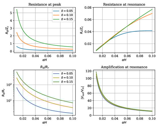
Figure 7.
Behavior of the helical resonator at the peak resistance and at the resonance, plotted as a function of the normalized attenuation factor , for three different values of the relative tap position . Top left: input resistance at peak, normalized to the characteristic impedance . Top right: input resistance at resonance, normalized to the characteristic impedance . Bottom left: ratio of the previous two quantities. Bottom right: voltage amplification factor .
We should now remark, though, that the input impedance at resonance is given by the following:
This expression clarifies that the input impedance at resonance is not fully resistive. Indeed, the point of zero phase is located at a slightly lower frequency. As a consequence, the calculation of the input impedance and of the amplification factor for the point of purely resistive input impedance has to be done numerically by identifying the wave number for which the imaginary part of the impedance is zero, and then evaluating its real part at this same wave number. It is instructive to plot the resistance at the point of purely resistive impedance near resonance and the voltage amplification at the same point as a function of the tap position for different attenuation factor values. This is depicted in Figure 8. On the same figures, the resistance (real part of the impedance) and the amplification factor computed precisely at resonance are shown as dashed lines. It is possible to observe that the resistance curves at resonance display a steep rise for low values of , a maximum, and then a slower fall. This behavior suggests that if one wants to work at resonance and a specific value of this resistance is sought (typically 50 for good matching), then one may wish to stay on the right of the peak, where the slow variation is forgiving in regards to imprecision in the construction. This also gives slightly higher voltage amplification than at very low values. Additionally, one should observe that if the dissipation is too low, then there exists the possibility that matching is not achievable because the input resistance is lower than that required for all possible values. However, if instead of working precisely at resonance, the nearby point of purely resistive input impedance is chosen, it can be seen that a monotonously decreasing resistance is found. In fact, for values that are sufficiently high, the curves superpose to those obtained at resonance, indicating a very small difference between the two points. A larger discrepancy appears at low , where the resistance at resonance decreases, while the other value increases steeply. In this same region, the amplification factor at the point of purely resistive impedance decreases with respect to the one at resonance. Generally speaking, it seems advisable to avoid the low values where a strong discrepancy of the two conditions appears, and where small errors in determining may translate to large changes in input resistance. For these values of the attenuation factor, this suggests a value of 0.1 or larger.
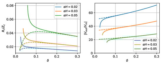
Figure 8.
Behavior of the helical resonator at the point of purely resistive input impedance near resonance (continuous line) and at resonance (dashed line), plotted as a function of the tap position , for three different values of the normalized attenuation factor . Left: input resistance at resonance, normalized to the characteristic impedance . Right: voltage amplification factor .
5. The Fully Shielded Helical Resonator
While the procedure described above constitutes the general approach, from now on, we want to focus on the condition , that is, with the shield directly superimposed to the helical coil. We shall call this case “fully shielded resonator”. This is the most interesting situation for plasma production, because in practical situations, especially for devices that are intended to be taken out of the laboratory, one wishes to minimize electromagnetic radiation, both for safety and electromagnetic compatibility reasons. Since a helical antenna, when operating at wavelengths much larger than its size, radiates mainly from the sides [26], the grounded shield should prevent this irradiation (hence its name). Furthermore, since radiation is one major source of dissipation, it is expected that the shielded resonator will have a lower . Thus, we think that a good construction practice is to always wrap the coil in a conducting grounded shield, with close proximity.
This situation makes also for easier calculations since, as seen above, no numerical solution is needed: and . This allows to recast in terms of the frequency the previously found expressions, which were given in terms of the wave number . Indeed, it is straightforward to show that in this case, the following holds:
The normalized frequency at which the peak in input resistance occurs is as follows:
We see that for a given coil diameter, this frequency is inversely proportional to the number of turns. It is also possible to normalize the frequency f to the frequency of maximum resistance , and write the following:
It is thus straightforward to replot the graphs in Figure 5 and Figure 6 as a function of . This is not the case for values of larger than 1, where the velocity factor is frequency dependent, and the transformation from wave number to frequency is nonlinear. The resonance frequency is related to by the following:
6. Effect of a Capacitive Load
In many practical applications, the helical resonator will not be free-standing, but its upper end will be connected to some electrode or other structure, adding to it a load that, in a first approximation, can be considered fully capacitive. Even when this is not the case, one may wish to measure the voltage of the upper end with a high voltage oscilloscope probe, which will add a capacitive load of capacitance C (typically a few pF). We thus wish to address the problem of connecting a load with impedance
to the transmission line model described above. Using a standard result of transmission line theory, the input impedance of a line of length L and characteristic impedance connected to a load is the following:
where is the reflection coefficient at the load, given by the following:
For the case of a capacitive load, the reflection coefficient takes the following form:
where the characteristic time is defined as follows:
The helical resonator can be considered the parallel of the bottom section and of the top section, the latter being connected to the capacitive load. Since the bottom section is short-circuited by the ground connection, it has and, therefore, , so its input impedance is . Combining this in parallel with the top section connected to the capacitive load, one obtains the overall input impedance as follows:
In the limit , tends to 1, and the formula for correctly reduces to expression (44).
Using the fact that
it is straightforward to derive the voltage amplification factor:
According to Corum et al., this is “probably the most important equation in all of high voltage RF engineering” [27]. Once again, when tends to 1, this formula reduces to expression (42).
Figure 9 shows, for a fully shielded resonator, the frequency dependence of the input impedance normalized to the characteristic impedance of the amplification factor, and of the phases between and and between and , for various values of . As before, the frequency is normalized to the frequency corresponding to the wave number , which satisfies , that is, the frequency of the maximum input impedance in the no-load case.
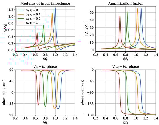
Figure 9.
Behavior of the fully shielded helical resonator with capacitive load plotted as a function of frequency f, normalized to the frequency of maximum impedance modulus, for different values of . The curves are computed for and . Top left: modulus of the input impedance normalized to the characteristic impedance . Top right: voltage amplification factor . Bottom left: phase shift in degrees between input voltage and input current. Bottom right: phase shift in degrees between the input voltage and the output voltage.
It is possible to observe that as the load capacitance is increased (and, therefore, becomes larger) the resonance frequency decreases, and the peak impedance and peak voltage amplification are both reduced. The phase diagrams are also shifted toward lower frequencies. In general, the downshift in frequency appears to be the most relevant effect, unless the capacity becomes too large.
We can now evaluate as before the input impedance and the amplification factor at the near-resonance frequency where the input impedance is real. The results are shown in Figure 10, for four different values of . We see that the curves have a shape similar to that shown in Figure 8, with a region with a strong gradient at low , difficult to practically use, and then a region of slowly varying and amplification factor. As the load capacitance is increased, the part with a steep gradient of the curves is shifted to the right, while the rest collapses onto a single curve, suggesting that the capacitive load does not affect the matching condition if one stays in this region. The amplification factor curves are shifted downward, indicating a reduction in voltage amplification caused by the increasing load. Since this gives a reduction in performance, care should be taken to avoid too large capacitance at the high voltage end of the resonator. If the resonator is to be connected to a system of electrodes, this should be taken into consideration.
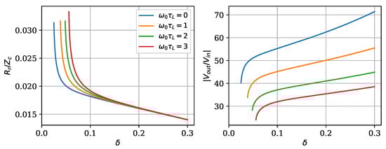
Figure 10.
Left: plot of the input resistance normalized to the characteristic impedance of the fully shielded resonator with capacitive load, achieved in the purely resistive condition near the resonance, as a function of the relative tap point position , for different values of . (Right): voltage amplification factor for the same conditions. The attenuation factor is .
7. Experimental Results
The theoretical results described up to now were checked against the properties of actual helical resonators, both with and without a conducting shield, in unloaded and loaded conditions. In these experiments, the input impedance was measured using a PocketVNA Vector Network Analyzer, in 1-port reflection only mode, which was properly calibrated. Furthermore, the voltage amplification factor at resonance was measured by sending RF power to the resonator and measuring the input voltage with a 10:1 oscilloscope probe and the output voltage with a 1000:1 Tektronix P6015a high voltage (HV) probe. For this latter experiment, the frequency was adjusted so as to achieve the maximum ratio.
The first resonator (resonator 1) was built, using a 1 mm diameter insulated wire wound on a polyurethane tube of a 10 mm inner diameter and 12 mm outer diameter. Initially, 110 turns of wire were wound, and the tap point was located after 10 turns (). By measuring the resonator axial length, the average pitch was evaluated to be 1.04 mm, in good agreement with the wire thickness. Subsequently, while the tap point was kept fixed, the number of turns on the top part of the resonator was decreased from 100 to 90, then to 80, and so on up to 60 ().
The resonator input impedance modulus and phase were measured using the VNA as a function of frequency. The results are shown in the top row of Figure 11. The curves were fitted with expression (44). However, this expression is given as a function of the wavenumber , which is related to the frequency by . Thus, in order to be able to perform a fit on the data given as a function of frequency, was replaced in expression (44) by , introducing the new parameter , which represents the frequency at which the electrical length of the entire resonator is equal to , i.e., the frequency where the maximum of the input impedance is located. The fit thus led to optimal values of the parameters , and , and then was computed as . In fact, is frequency dependent, and this dependence should be included in the fit. However, this would lead to a complex procedure, due to the need to solve the eigenvalue equation at each step. It was thus decided to assume to be almost constant in the vicinity of the resonance. It can be seen that the resulting curves fit reasonably well with the experimental ones, both for the amplitude and the phase of the input impedance.
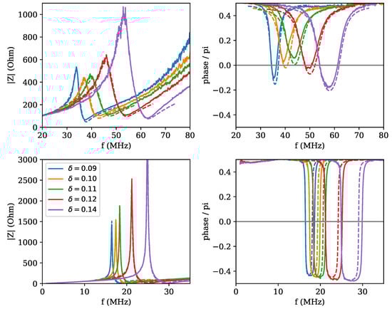
Figure 11.
(Top): plot of the modulus (left) and phase (right), normalized to , of the input impedance of resonator 1. The different curves correspond to different number of turns above the tap point. The dashed curves are the fits obtained as described in the text. Bottom: same as above, but with the addition of a conducting shield around the resonator.
Subsequently, a grounded shield made from an aluminum tube with an internal diameter of 16 mm and external diameter of 18.3 mm (average diameter of 17.15 mm and thickness of 2.3 mm) was applied to the resonator, and the fitting procedure was repeated as shown in the bottom row of Figure 11. The fitting curves also follow reasonably well the experimental ones. It can be noted that the curves for the shielded resonator are much sharper with stronger gradients, and the phases reach more negative values at the resonance, all indications of a reduced dissipation. This can be understood by assuming that the main source of dissipation is radiation from the sides of the device, which is prevented by the conducting screen. In this respect, it is important to notice, for experimenters wishing to repeat this work, that the wire used to ensure the grounding of the shield should be positioned so as to minimize the formation of loops, which can act as antennas.
The resulting values of the fit parameters, both without and with shield, are shown in Figure 12. It can be seen that the characteristic impedance without shield grows with from 1.15 k to 1.3 k, whereas with the shield, it has a constant value of around 580 . The attenuation factor turns out to have a peaked shape, with values ranging between 0.05 and 0.11. This shape is somehow surprising: indeed, as is increased by reducing the number of turns on the top end, and therefore the resonator length H, one would expect a decreasing behavior of with , assuming to be a constant independent of the resonator size. It is, however, possible that other issues enter the dissipation process, including possible different cable positions, and therefore different radiation patterns between one measurement and the following. This is also in agreement with the observation that in the shielded case, the obtained value of is constant, around 0.0085. If one assumes that the shield suppresses radiation, then this residual value could be attributed to other causes, and the case-to-case variation would disappear. The frequency was found to be linearly increasing with , both for the unshielded and shielded case. This was expected, in view of a constant velocity factor. Indeed, the velocity factor turns out to be essentially constant, with a value of 0.052 for the unshielded case and 0.024 for the shielded one.
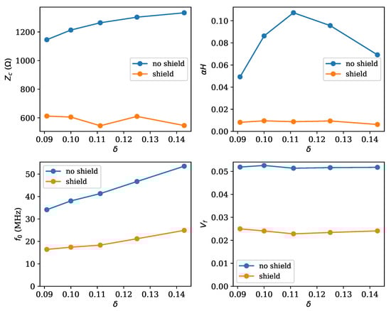
Figure 12.
Parameters resulting from the fits of the input impedance data for resonator 1, plotted as a function of the relative distance of the tap point from the bottom end. Top left: characteristic impedance. Top right: attenuation parameter. Bottom left: frequency at which the total electrical length of the resonator is . Bottom right: velocity factor, obtained from the previous quantity. In all graphs, results without and with conducting shield are reported.
An important issue to be addressed is how much the characteristic impedance (for the unshielded case) and the velocity factors match the predictions of the propagation model described in Section 3. According to expression (28), one would expect in the unshielded case a characteristic impedance of 2.25–2.45 k at the frequency where the resonance occurs in the measurements. This is more or less double than what was found from the fits. Concerning the velocity factor, from expression (25) one would expect values of 0.07 for the unshielded case, and 0.036 for the shielded one. These are both 1.5 times larger than those found from the fits. The source of these discrepancies is not clear.
Subsequently, two other resonators were built (resonators 2 and 3) with a fixed number of turns (10 and 100 for the bottom and top parts, respectively), wound on quartz tubes. The tube of resonator 2 had a diameter of 12 mm, whereas the tube of resonator 3 had a diameter of 7 mm. The length H was respectively 110 mm and 103 mm. The shield was obtained from the same aluminum tube, which was used to shield resonator 1. Their input impedance was once again measured, using the Pocket VNA instrument. Since in this experiment, the aim was to measure the high voltage generated at the resonator open end, using a Tektronix P6015A high voltage probe, the input impedance measurements were performed both with and without the probe attached to the resonator. Indeed, the probe is expected to add a capacitive load, along the lines described in Section 6. The nominal HV probe input capacitance is, according to the technical specifications, around 3 pF.
The results of the measurements are shown in Figure 13 for resonator 2 and in Figure 14 for resonator 3. In both cases, the addition of the probe causes a downshift in frequency of the resonance pattern, both for the case without the shield (top row) and for the shielded case (bottom row). Again, the curves for the shielded case appear sharper, indication of a lower dissipation. The fitting procedure adopted is the following: at first, the curves without HV probe were fitted as described above. Subsequently, the curves obtained with the HV probe attached to the resonator open end were fitted, using expression (59), but keeping the values of and fixed to those resulting to the previous fit, and adjusting only and the new parameter . While, in principle one would think that also should be kept constant—and this was tried at the beginning—it was realized that it was not the case, possibly due to novel radiation sources stemming from the new layout.
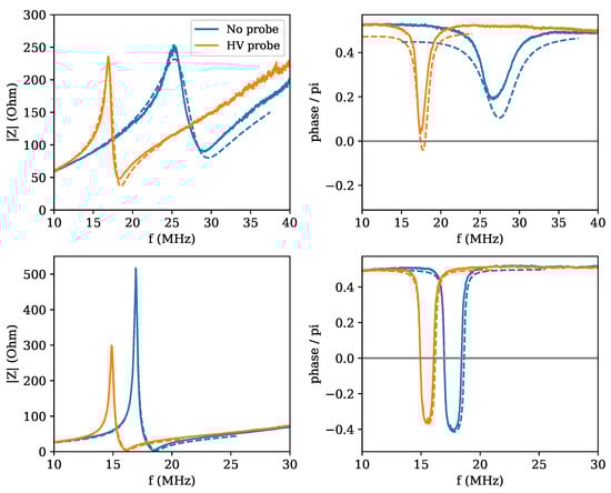
Figure 13.
Top: plot of the modulus (left) and phase (right), normalized to , of the input impedance of resonator 2, both in standard configuration and with the HV probe attached to the open end. The dashed curves are the fits obtained as described in the text. Bottom: same as above, but with the addition of a conducting shield around the resonator.
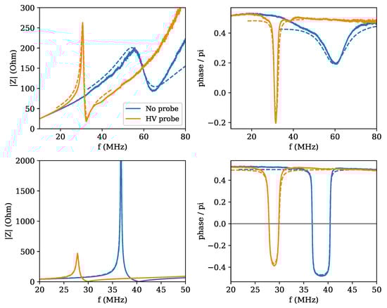
Figure 14.
Top: plot of the modulus (left) and phase (right), normalized to , of the input impedance of resonator 3, both in standard configuration and with the HV probe attached to the open end. The dashed curves are the fits obtained as described in the text. Bottom: same as above, but with the addition of a conducting shield around the resonator.
The results shown in Figure 13 for resonator 2 demonstrate that the model for the loaded resonator is actually very good. Indeed, the quality of the fit appears to be even better than for the resonator in standard conditions, suggesting that also in this case, some parasitic capacitance should be taken into account. Only the phases for the unshielded case show some discrepancy, mainly due to the experimental curves in the regions away from the resonance being somehow higher than the expected value. This is likely due to some instrumental error, which is not unlikely, given that the Pocket VNA is a low-cost instrument. Similar considerations apply also to the curves depicted in Figure 14, which refer to resonator 3.
The results of the fits for the two resonators are summarized in Table 1. It can be seen that a characteristic impedance of about 1 k was found for both resonators, which was then reduced to one quarter and to a half, respectively, when the shield was placed. The strong reduction in dissipation in the shielded case was confirmed. It is, however, to be noticed that also the placement of the HV probe on the high voltage end led to a reduction in dissipation, something which is not yet fully understood but which may depend on the radiation pattern. It is remarkable to observe that in the case of resonator 3, both measurements with the HV probe, with and without shield, led to a load capacitance of around 4 pF, not dissimilar to the nominal value of 3 pF. In the case of resonator 2, two slightly higher, and different, values of 5 and 7 pF were found. It is, however, to be noticed that the quality of contacts and other issues, such as the proximity of the work bench surface, may add parasitic capacitance. It is nevertheless remarkable that the correct order of magnitude could be obtained.

Table 1.
Parameters resulting from the fit of the input impedance curves for resonators 2 and 3. The load characteristic time and the associated load capacitance C are also reported.
Concerning the comparison with the predictions of the propagation model of Section 3, for resonator 2 in the unshielded configuration, the model overestimates the characteristic impedance by a factor 2.8 and the velocity factor by a factor 2.6, while in the shielded case, the overestimate is by a factor 1.9. For resonator 3 in the unshielded configuration, there is an overestimation of the characteristic impedance by a factor of 1.6 and of the velocity factor by a factor of 2.2, whereas in the shielded case, the velocity factor is overestimated by a factor 1.9. Overall, these results confirm that the propagation model needs to be somehow updated to better match the experimental results.
The voltage amplification factor was measured for both resonators 2 and 3 by tuning the frequency on the resonance, that is, on the condition of maximum amplification. The output voltage was measured, using the Tektronix P6015A high voltage probe, whereas the input voltage was measured with a standard x10 oscilloscope probe, which was tested and shown not to alter significantly the circuit behavior. The resulting voltage amplification factors, for both resonators 2 and 3, unshielded and shielded, are given in Table 2, where they are compared with the predicted values given by , with resulting from the fits. It can be seen that a reasonable agreement is achieved, confirming that the modeling described above is adequate to predict the performance of a given resonator. It should be emphasized that, as expected from the fit results, the best performance is given by the shielded resonators. In particular, resonator 3 achieved a voltage amplification of 100, while resonator 2 achieved a value of 80. In this latter case, this resulted in an actual measured of 4.3 kV—more than appropriate to ionize most gases in a wide pressure range. It is to be remarked that the actual output voltage will depend on the input one, which in itself will be determined by the power of the amplifier used as the power source, and by the input impedance.
Table 2.
Comparison of the experimental amplification factor at resonance with the expected value predicted from the fit outcome, for resonators 2 and 3, with and without shield.
8. Conclusions
The production of RF plasmas requires both a good matching of the load to the power supply and a method to magnify the voltage so as to achieve the gas breakdown. The shielded helical resonator excited at a tap point near the grounded end is a concept that allows, in principle, to achieve both goals, allowing a very simple construction for the plasma source and a direct connection to the generator, without the need for a fault-prone matching network. However, in order to achieve both goals, a proper design is needed. In this paper, we derived formulas that allow a prediction of the resonator performance, thus enabling the plasma scientist to properly design his source according to the parameters required for his plasma, and we have tested them experimentally.
Clearly, what is missing in this treatment is the effect of the plasma itself, once it is ignited. This puts an additional load on the resonator, and it is to be evaluated how much it can bring the operational conditions away from the optimal ones, especially in relation to the reflected power. This will be the topic of a subsequent study.
Similarly, the results concerning the treatment of the resonator as a transmission line depend on the characteristic impedance, which, for the moment, can be explicitly calculated only for the shieldless case and needs to be measured experimentally in all other situations, particularly for the fully shielded resonator. Furthermore, even in the shieldless case, it was found that the formula gave a result different from the experimental one by a factor of two, something which needs to be better investigated.
It is also to be remarked that to date, we have implicitly considered a capacitively coupled plasma source, where the amplified voltage gives rise to an electrostatic field, inducing breakdown. However, the very nature of the helical resonator makes it suitable also for the transition to an inductive regime [28]. This possibility and the effects on the load need also to be investigated.
In conclusion, it is our belief that a renewed interest in the helical resonator concept could lead to new, simpler and more compact designs for RF plasma sources, increasing the efficiency and the reliability. Furthermore, the concept of a circuit element where the lumped circuit approximation fails and the pattern and speed of voltage propagation become important, is in itself a stimulating and non-trivial idea that should be more widely taught in plasma technology courses.
Author Contributions
Conceptualization, E.M., R.C., L.C. and M.Z.; methodology, E.M.; software, E.M.; validation, R.C., L.C. and M.Z.; writing—original draft, E.M.; writing—review and editing, E.M., R.C., L.C. and M.Z.; visualization, E.M.; supervision, E.M. All authors have read and agreed to the published version of the manuscript.
Funding
This research received no external funding.
Conflicts of Interest
The authors declare no conflict of interest.
Abbreviations
The following abbreviations are used in this manuscript:
| RF | Radio Frequency |
| HV | High Voltage |
Appendix A. Transmission Line Theory
We recall here the basic concepts of transmission line theory. A transmission line is characterized by four distributed line parameters: the resistance per unit length R, the inductance per unit length L, the capacitance per unit length C and the conductance per unit length G of the dielectric separating the two conductors of the line.
The general solution at an angular frequency for the voltage and current along a line, composed of the superposition of a forward-propagating wave and a backward-propagating one is the following:
where x is a coordinate running along the line, with being the attenuation constant and the wave number of the propagating perturbations, and is the characteristic impedance of the line. These quantities are defined by the distributed line parameters, in the limit and , by the following:
where the characteristic impedance and the phase velocity are given by the following:
It is worth noting that, if G is negligible,
The actual values of the distributed parameters are difficult to predict from the specifications of the line for non-trivial geometries, so it seems better to consider (or the velocity factor ), and as unknown parameters and derive them either by studying the propagation properties of the line or by the fitting of the experimental data. The attenuation coefficient , however, remains still undetermined, and cannot be trivially computed from Equation (A5) because the resistance per unit length can be substantially different from the DC value and must be evaluated experimentally.
The reflection coefficient of the line is a position-dependent quantity defined as follows:
The wave impedance is another position-dependent quantity defined as follows:
Recalling the definition of the reflection coefficient, we have the following:
The reflection coefficient can be written in terms of impedance as follows:
Voltage and current can be written in terms of the reflection coefficient as follows:
References
- Cvetic, J.M. Tesla’s high voltage and high frequency generators with oscillatory circuits. Serbian J. Electr. Eng. 2016, 13, 301–333. [Google Scholar] [CrossRef] [Green Version]
- Macalpine, W.W.; Schildknecht, R.O. Coaxial resonators with helical inner conductor. Proc. IRE 1959, 47, 2099–2105. [Google Scholar] [CrossRef]
- Niazi, K.; Lieberman, M.A.; Lichtenberg, A.J.; Flamm, D.L. Operation of a helical resonator plasma source. Plasma Sources Sci. Technol. 1994, 3, 452–465. [Google Scholar] [CrossRef]
- Welton, R.F.; Thomas, E.W.; Feeney, R.K.; Moran, T.F. Simple method to calculate the operating frequency of a helical resonator-RF discharge tube configuration. Meas. Sci. Technol. 1991, 2, 242–246. [Google Scholar] [CrossRef]
- Hopwood, J. Review of inductively coupled plasma for plasma processing. Plasma Sources Sci. Technol. 1992, 1, 109–116. [Google Scholar] [CrossRef]
- Bongkoo, K.; Park, J.C.; Kim, Y.H. Plasma Uniformity of Inductively Coupled Plasma Reactor with Helical Heating Coil. IEEE Trans. Plasma Sci. 2001, 29, 383–387. [Google Scholar] [CrossRef]
- Siverns, J.D.; Simkins, L.R.; Weidt, S.; Hensinger, W.K. On the application of radio frequency voltages to ion traps via helical resonators. Appl. Phys. B 2012, 107, 921–934. [Google Scholar] [CrossRef] [Green Version]
- Medhurst, R.G.H.F. resistance and self-capacitance of single layer solenoids. Wirel. Eng. 1947, 24, 35–43. [Google Scholar]
- De Miranda, C.M.; Pichorim, S.F. Self-resonant frequencies of air-core single-layer solenoid coils calculated by a simple method. Electr. Eng. 2015, 97, 57–64. [Google Scholar] [CrossRef]
- Everard, J.K.A.; Cheng, K.K.M.; Dallas, P.A. High-Q helical resonator for oscillators and filters in mobile communication systems. Electron. Lett. 1989, 25, 1648–1650. [Google Scholar] [CrossRef]
- Antoniuk, J.; Żukociński, M.; Abramowicz, A.; Gwarek, W. Investigation of Resonant Frequencies of Helical Resonators. In Proceedings of the 11th Microcoll, Budapest, Hungary, 10–11 September 2003; p. 5. [Google Scholar]
- Blažević, Z.; Poljak, D. Some notes on transmission line representations of Tesla’s transmitters. In Proceedings of the 16th International Conference on Software, Telecommunications and Computer Networks, Split, Croatia, 25–27 September 2008; pp. 60–69. [Google Scholar]
- Bletzinger, P. Dual mode operation of a helical resonator discharge. Rev. Sci. Instrum. 1994, 65, 2975. [Google Scholar] [CrossRef]
- Deng, K.; Sun, Y.L.; Yuan, W.H.; Xu, Z.T.; Zhang, J.; Lu, Z.H.; Luo, J. A Modified Model of Helical Resonator with Predictable Loaded Resonant Frequency and Q-Factor. Rev. Sci. Instrum. 2014, 85, 104706. [Google Scholar] [CrossRef] [PubMed]
- Deri, R.J. Dielectric measurements with helical resonators. Rev. Sci. Instrum. 1986, 57, 82. [Google Scholar] [CrossRef]
- Yang, J.H.; Zhang, Y.; Li, X.M.; Li, L. An improved helical resonator design for rubidium atomic frequency standards. IEEE Trans. Instrum. Meas. 2010, 59, 1678. [Google Scholar] [CrossRef]
- Zhu, J.W.; Hao, T.; Stevens, C.J.; Edwards, D.J. Optimal design of miniaturized thin-film helical resonators. Appl. Phys. Lett. 2008, 93, 234105. [Google Scholar] [CrossRef]
- Ollendorf, F. Die Grundlagen der Hochfrequenztechnik; Springer: Berlin, Germany, 1926; pp. 79–87. [Google Scholar]
- Sichak, W. Coaxial Line with Helical Inner Conductor. Proc. IRE 1954, 42, 1315–1319. [Google Scholar] [CrossRef]
- Sensiper, S. Electromagnetic Wave Propagation on Helical Structures (A Review and Survey of Recent Progress). Proc. IRE 1955, 43, 149–161. [Google Scholar] [CrossRef]
- Uhm, H.S.; Choe, J.-Y. Properties of the electromagnetic wave propagation in a helix-loaded waveguide. J. Appl. Phys. 1982, 53, 8483. [Google Scholar] [CrossRef]
- Anicin, B.A. Plasma loaded helical waveguide. J. Phys. D Appl. Phys. 2000, 33, 1276–1281. [Google Scholar] [CrossRef]
- Niazi, K.; Lichtenberg, A.J.; Lieberman, M.A. The dispersion and matching characteristics of the helical resonator plasma source. IEEE Trans. Plasma Sci. 1995, 23, 833. [Google Scholar] [CrossRef]
- Corum, K.L.; Corum, J.F. RF coils, helical resonators and voltage magnification by coherent spatial modes. In Proceedings of the 5th International Conference on Telecommunications in Modern Satellite, Cable and Broadcasting Service. TELSIKS 2001. Proceedings of Papers (Cat.No.01EX517), Nis, Yugoslavia, 19–21 September 2001; Volume 1, p. 339. [Google Scholar]
- Park, J.-C.; Kang, B. Impedance model of helical resonator discharge. IEEE Trans. Plasma Sci. 1997, 25, 1398–1405. [Google Scholar] [CrossRef]
- Kraus, J.D. The helical antenna. Proc. IRE 1949, 37, 263–272. [Google Scholar] [CrossRef]
- Corum, J.; Daum, J.; Moore, H.L. Tesla Coil Research; Contractor Report ARCCD.CR-92006; U.S. Army Armament Research, Development and Engineering Center: Picatinny, NJ, USA, 1992. [Google Scholar]
- Park, J.-C.; Lee, J.K.; Kang, B. Properties of inductively coupled plasma source with helical coil. IEEE Trans. Plasma Sci. 2000, 28, 403–413. [Google Scholar] [CrossRef]
Publisher’s Note: MDPI stays neutral with regard to jurisdictional claims in published maps and institutional affiliations. |
© 2021 by the authors. Licensee MDPI, Basel, Switzerland. This article is an open access article distributed under the terms and conditions of the Creative Commons Attribution (CC BY) license (https://creativecommons.org/licenses/by/4.0/).