Article

Wide Scanning Angle Millimetre Wave 1 × 4 Planar Antenna Array on InP at 300 GHz

Institute for Systems and Computer Engineering, Technology and Science (INESC TEC) and Faculty of Engineering, University of Porto, 4200-465 Porto, Portugal
*
Author to whom correspondence should be addressed.
Appl. Sci. 2021, 11(15), 7117; https://doi.org/10.3390/app11157117
Submission received: 2 July 2021 / Revised: 23 July 2021 / Accepted: 26 July 2021 / Published: 31 July 2021
(This article belongs to the Special Issue Terahertz Communications)

Abstract

:

Featured Application

Short-range millimetre wave communications.

Abstract

The design of a uniformly spaced 1 × 4 linear antenna array using epitaxial layers of benzocyclobutene over an InP substrate is demonstrated. The array elements are conjugately matched with a uni-travelling carrier photodiode at the input. The phased array is optimised to counteract mutual coupling effects by introducing metal strips with isolated ground planes for each radiating element. The proposed antenna array can provide a gain of 10 dBi with a gain variation of ±3 dB. The array operates over a bandwidth of 10 GHz (295–305 GHz) with a wide scanning angle of 100° in the broadside.

1. Introduction

Millimetre-wave (mm-wave) communications provide an enormous potential for revolutionising mobile communications in terms of data rates and bandwidth. These systems were in use for security applications for more than two decades [1], and the recent introduction of sub-THz bands in 5G standards [2] has sparked an increased interest in the research community. Yet, the challenges of generation and path loss of sub-THz signals have always limited their use for communications applications. Millimetre-wave systems often rely on III-V compounds to develop and fabricate components such as amplifiers, oscillators and mixers [3,4,5,6]. The passive interconnection of mm-wave components is limited to waveguide structures (planar or non-planar) [7]. Moreover, sub-THz signals experience a propagation loss of approximately 100 dB for a transmission distance of just 10 m, imposing stringent power requirements on the link budget. As the output power of millimetre-wave sources is typically insufficient, directive arrangements, such as phased arrays, are often employed to constructively combine the output power from multiple generators so that the energy is radiated along a preferential direction in space.
Recently introduced microwave photonic techniques [8,9] have been key enabling technologies for millimetre-wave signal generation and processing. Photonics has long used III-V compounds such as gallium arsenide (GaAs) and indium phosphide (InP) as the base materials for the fabrication of active components such as laser sources, photodiodes and modulators. The electro-optical conversion of a signal has made it possible to perform signal operations, such as up/down conversion, delaying, filtering and Mux/Demux, in the optical domain [10,11,12,13], e.g., a sub-THz electrical signal can be retrieved by taking advantage of the heterodyne beating of an optical local oscillator and a modulated optical signal in a high-speed photodiode. The handling of signals in the optical domain has provided the ability to simplify the transceiver chain and harness the sizeable fractional bandwidth of optical components compared to their electronic counterparts. Sharing the same base material for optical and electrical components opens the possibility of sharing the same die for realising a complete on-chip sub-THz transceiver without the need for interconnects, as in the case of photodiodes (photomixing) for the generation of mm-wave frequencies using uni-travelling carrier photodiode (UTC-PD).
Typically, the electrical output power of integrated photodiodes is in the order of microwatts [3,14,15,16]. Due to the high path loss suffered by millimetre wave signals, an array of photodiodes is needed to transmit effectively even over a short distance. For an effective sub-THz transmitter/receiver, a phased array antenna is often utilised. An array of planar radiating elements can steer the beam along the desired direction and concentrate energy into the receiver. Sub-THz antenna arrays are conventionally implemented using non-planar structures such as horn antennas [17]. Array arrangements, whilst providing the desired performance measures (in terms of peak realised gain, impedance matching and bandwidth), are bulky and unsuitable for an integrated solution. Additionally, planar array structures on III-V substrates, especially InP, present serious design challenges. The InP has an isotropic etching profile, making it challenging to realise waveguiding structures involving via through holes. These design bottlenecks can be overcome by resorting to an alternative technique of depositing a thin film of a material having a lower relative dielectric constant over a ground plane that provides shielding to the InP substrate [18]. This superficial layer can be used to realise planar arrays by capacitively feeding the radiating elements. Previously reported planar arrays [17,18] were designed for an input impedance of 50 Ω, which is not typically the case for on-chip photodiodes.
Here, we present a linear 1 × 4 phased array designed on InP through the employment of layers of benzocyclobutene (BCB) deposited over a ground plane. The designed array provides a front-end for a microwave photonics-based sub-THz transceiver. The input impedance of radiating elements is optimised to provide a conjugate match to in-house-built uni-travelling carrier photodiodes operating at around 300 GHz for maximum power transfer. A capacitive feed structure is used to couple the mm-wave signal to the radiating patch and simultaneously provide the targeted impedance matching. The presented phased array is optimised to counteract mutual coupling effects by implementing parasitic metal strips with isolated ground planes (MSWIGP) for each radiating element. The 1 × 4 linear array provides a gain of 10 dBi with a wide scanning angle of 100° and an impedance matching bandwidth of 10 GHz (295 GHz–305 GHz). Using integrated true time delay phase shifters, the beam direction can be steered in broadside for ±50°.

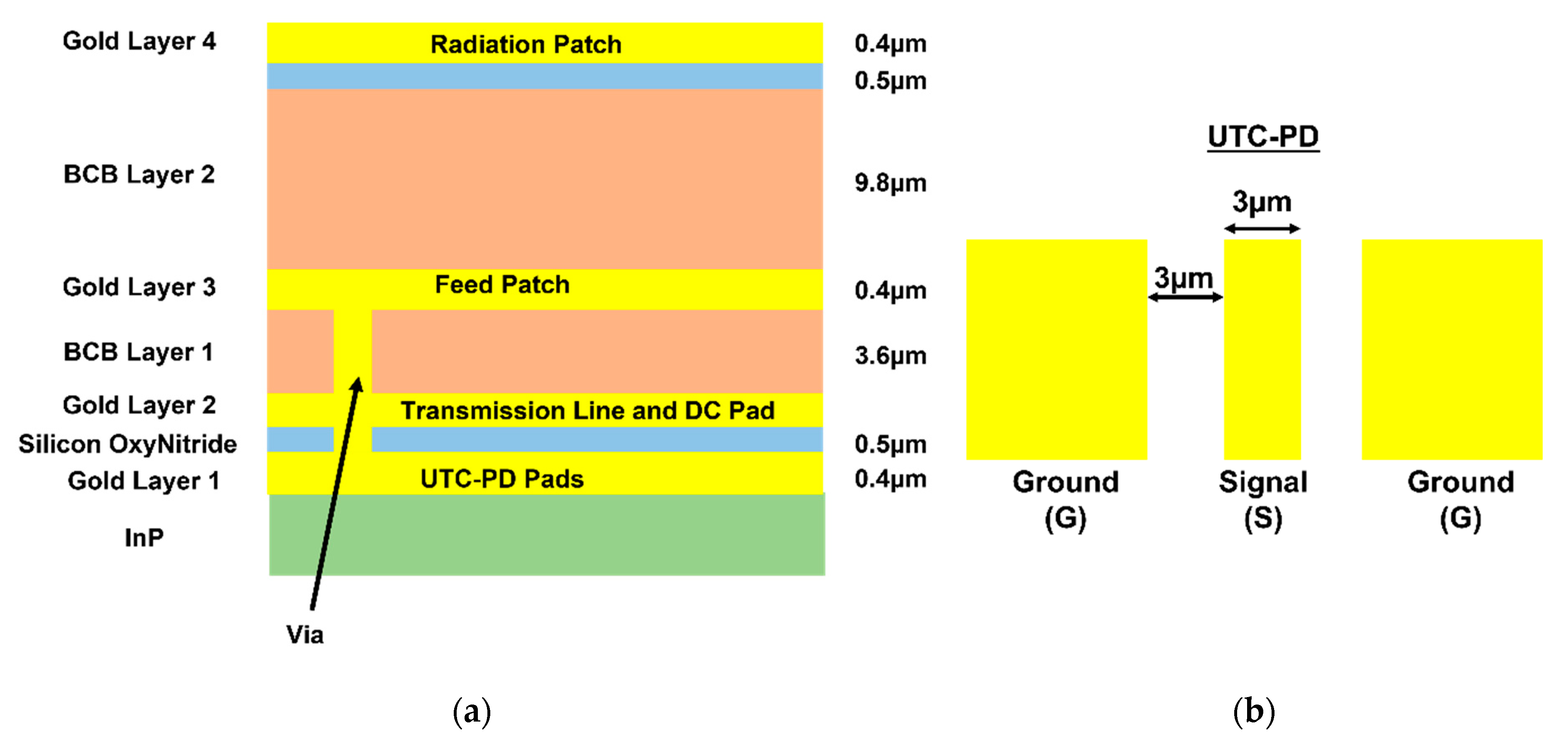
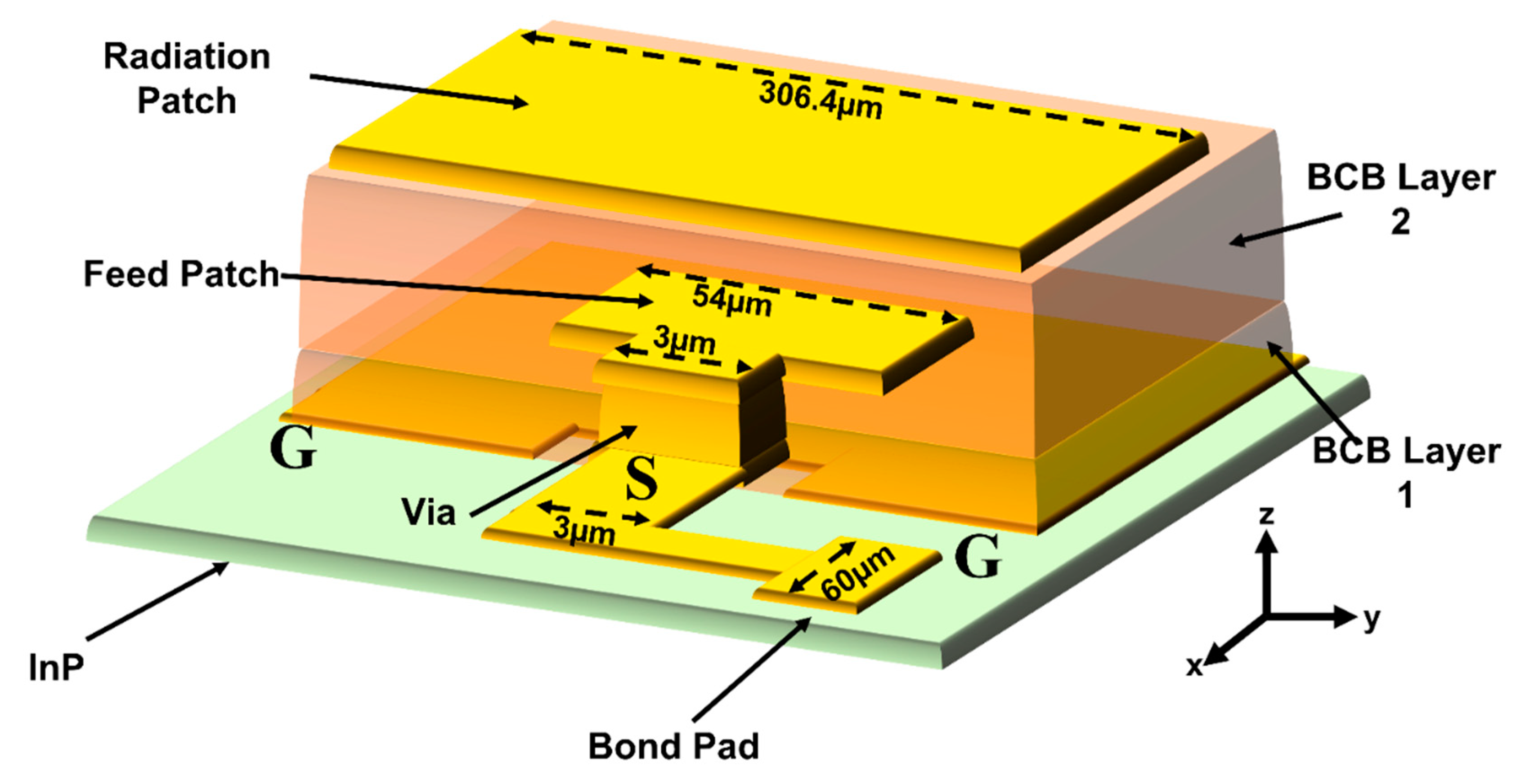
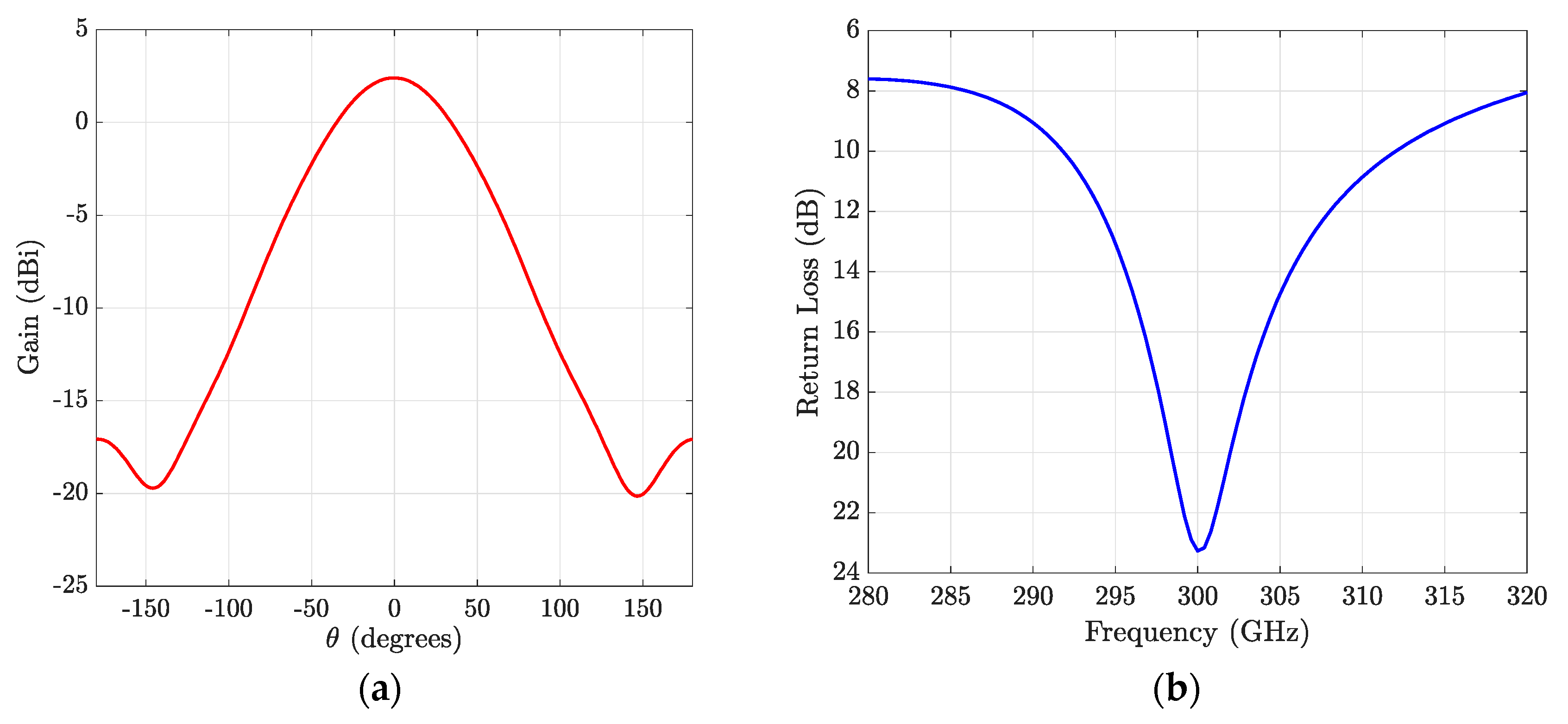
2. Design of the Unit-Cell
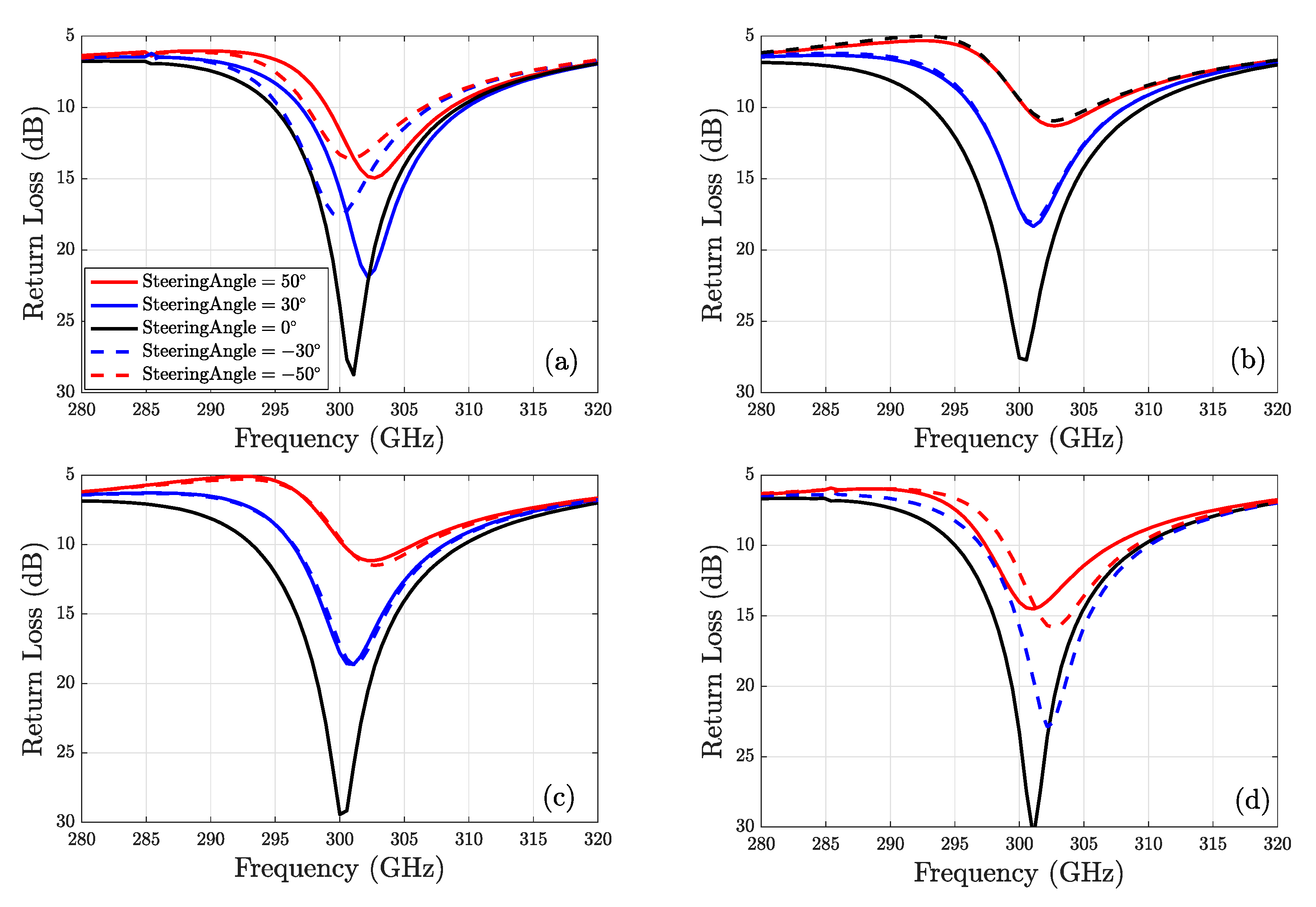
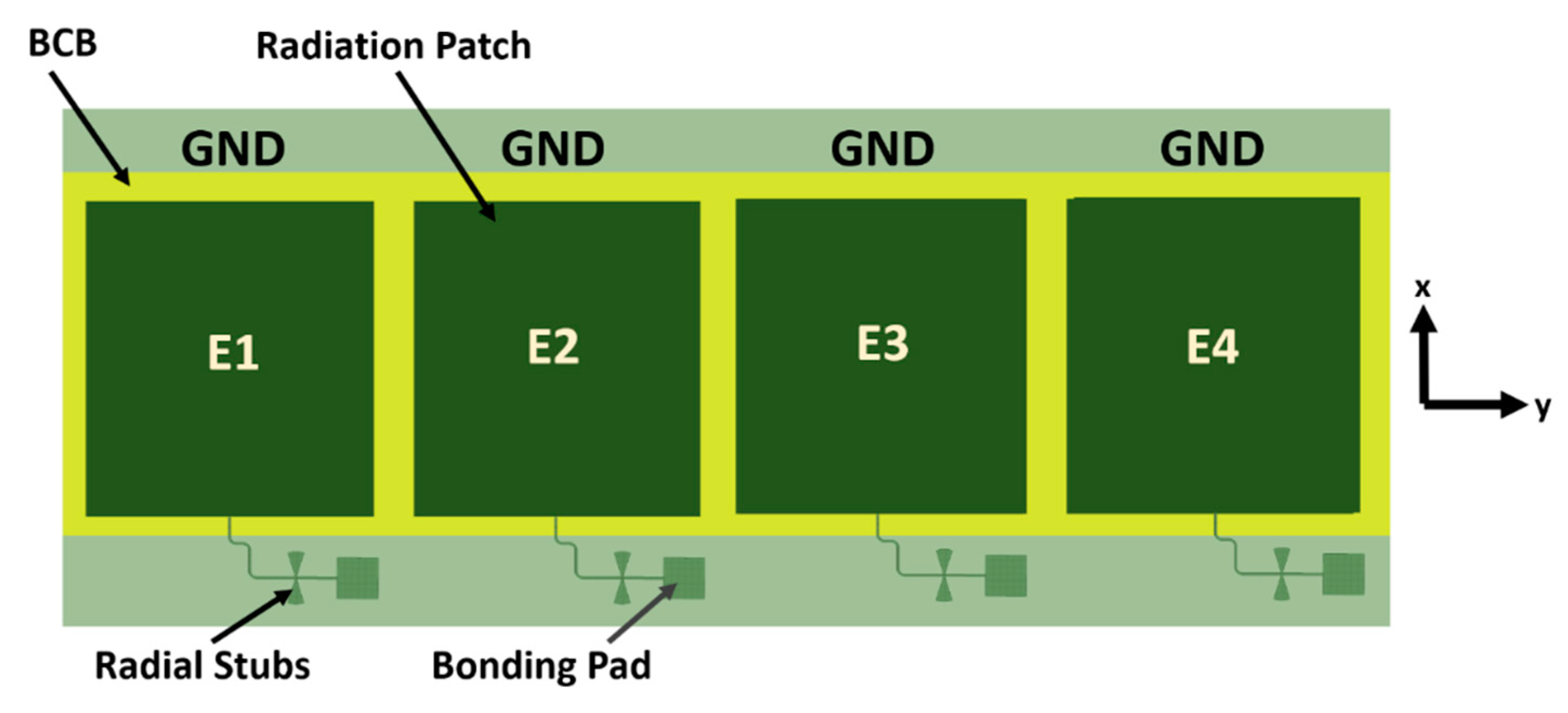
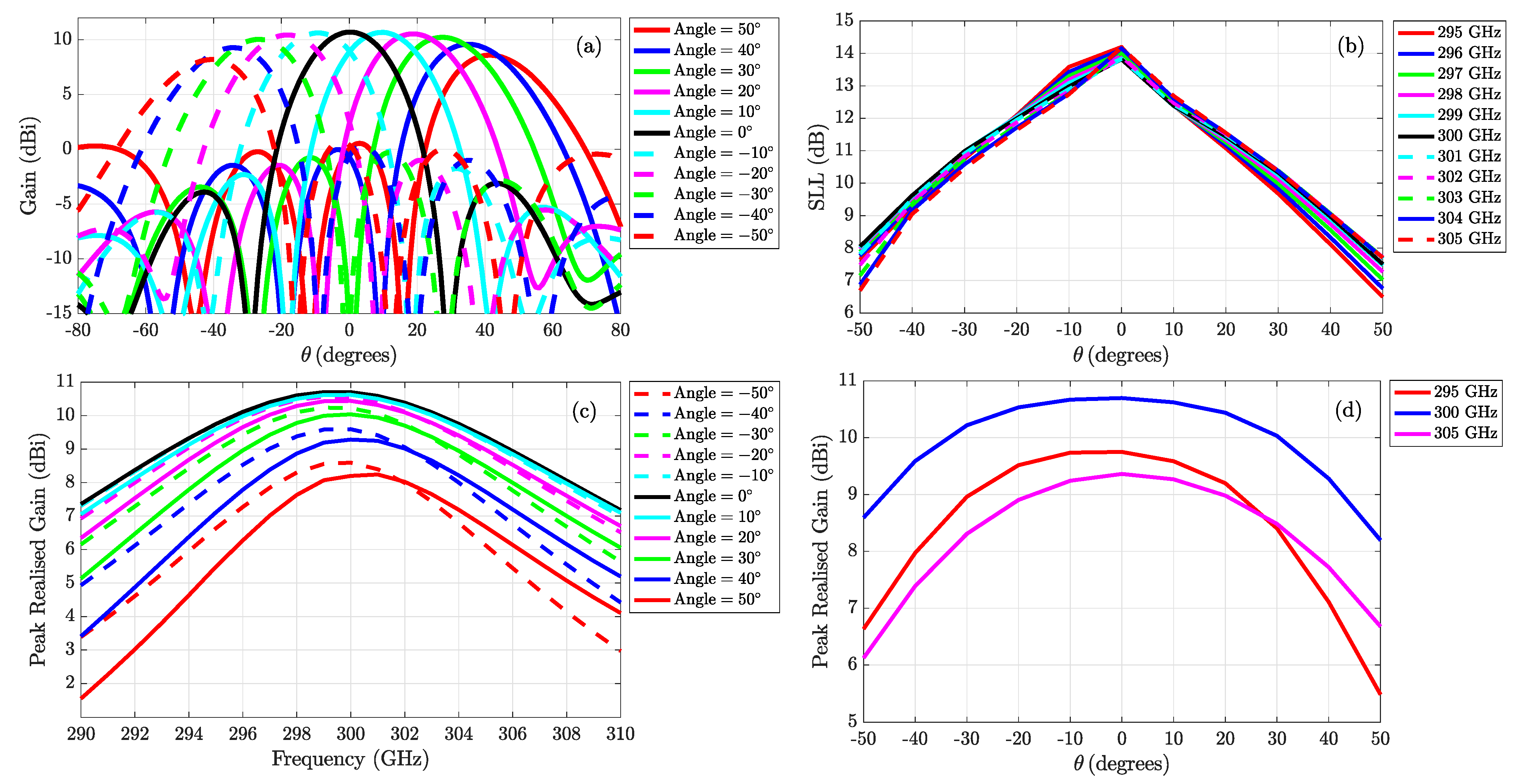
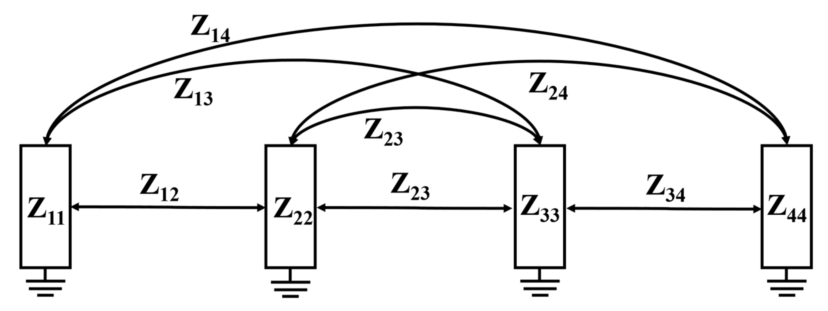
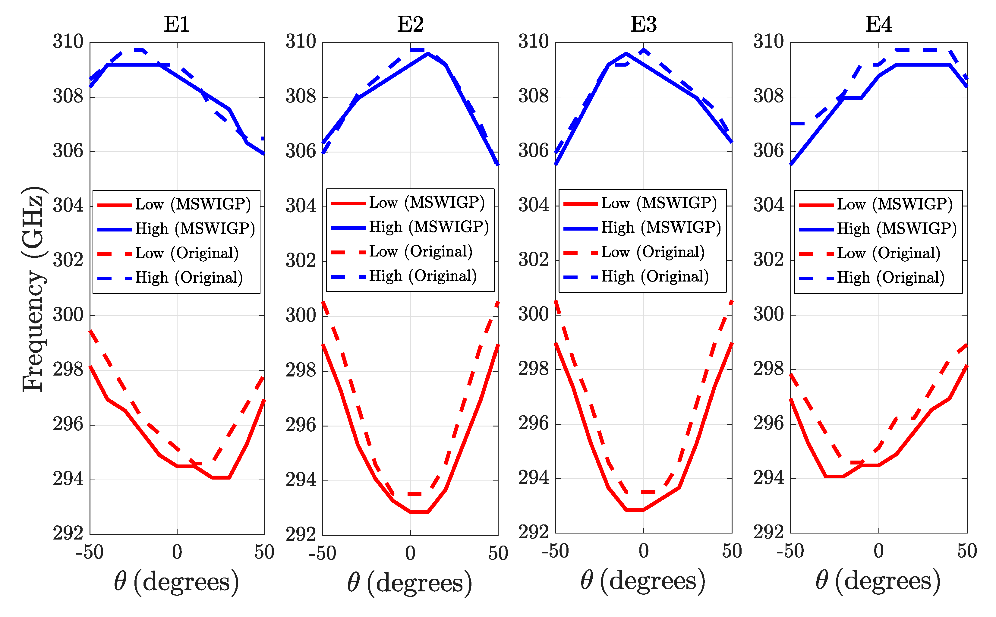
Based on the capacitive feed coupling technique presented in [19], a unit radiating element (also referred as unit-cell) is designed such that the input impedance is a conjugate match of the output impedance of a UTC-PD. The developed UTC-PD presents a complex output impedance of 15 + j8 Ω. In order to provide a conjugate matching, the input port impedance of the antenna structure is defined as 15 − j8 Ω.
The UTC-PD has a ground-signal-ground (GSG) output. Therefore, the signal pad is connected to the top feed patch employing a via etched in the epitaxially grown BCB Layer 1 (see Figure 1a) on top of a large gold ground plane deposited using Gold Layer 1. The BCB is a low-k dielectric compatible with InP processes which has a relative dielectric constant (ε) of 2.3 @ 300 GHz with a loss tangent (δ) of 0.01. It provides the ability to realise antenna elements over an InP substrate. The ground plane shields the mm-wave signal from back-radiating through a high dielectric constant InP substrate underneath. The epitaxial layer stack-up is shown in Figure 1a. A single 4 µm thick via is etched through the BCB Layer 1 with the same dimensions as the signal pad (Figure 1b).
On top of BCB Layer 1, a gold feed patch is deposited. A thin layer of silicon oxynitride (SiOxN) is also deposited between the Gold Layer 1 and Gold Layer 2 to implement the biasing circuit. The SiOxN layer increases the adhesion between Gold and BCB and provides a substrate layer between the biasing structure and the ground. The biasing circuit is implemented based on a microstrip line with two radial stubs acting as a shorting capacitor for the mm-wave signal. The microstrip connects to a bonding pad of 60 µm × 60 µm. The square radiation patch is deposited on top of a 10 µm thick BCB Layer 2 with dimensions of 306.4 µm × 306.4 µm. The planar dimensions of BCB layers are 500 µm × 500 µm; the size of the unit cell is increased in the x-direction by 100 µm to provide bonding pads for DC biasing and ground. The structure of the unit cell is presented in Figure 2.
The unit cell was simulated using Ansys HFSS v17. The simulated gain along θ (angle relative to the z axis) and return loss assuming a port impedance of 15 − j8 Ω are presented in Figure 3. The unit cell can provide a gain of 2.5 dBi with a matched impedance bandwidth of 10 GHz.

Array Design

By using the unit cell, a linear, uniformly spaced 1 × 4 array was also designed. The total area of the array is 2 × 0.6 mm2. The top view of the designed array is shown in Figure 4. Such an array can provide a gain of 10.85 dBi with a steering angle scanning range of 100°. The proximity of the radiating elements alters the boundary conditions of the unit-cell. This effect can be observed by plotting the active reflection coefficient for each unit-cell for different steering angles. For a steering angle of 0°, or when no phase shift is applied between elements, it can be observed that all the four radiating elements present an identical reflection coefficient across the whole bandwidth (Figure 5). As the phase shift between the driving signals of each element increases, the impedance matching bandwidth deteriorates. For extreme angles, i.e., ±50°, the array provides a bandwidth of merely 4–5 GHz, and the central elements are not matched at frequencies below 300 GHz. In Figure 6a,b, the beam steering pattern and sidelobe levels (SLL) are plotted as a function of frequency and steering angle. The SLLs shown in Figure 6b are asymmetric for varying steering angles. A signal with a wide bandwidth will be subjected to non-uniform gain and grating lobes at different frequencies, which can result in channel degradation and signal transmission loss. The peak realised gain (where realised gain is the gain of an antenna reduced by the losses due to mismatch of the antenna input impedance to a specified impedance [20]) shown in Figure 6c,d is not symmetric for positive and negative steering angles, indicating that the gain performance will not be uniform across the entire scanning range. The gain of the array will be significantly impacted for higher frequencies.
Thus, a signal centred around 300 GHz will experience a non-uniform response, and consequently a drop in performance.
The problem of mutual coupling is complex due to the dependence of the array’s parameters on the phase of the driving signal. A circuit model of mutual impedance is presented in Figure 7. The impedance Zij (where ij) has two components, i.e., static and dynamic. The static part of Zij is caused by a shared ground plane and the propagation of substrate waves. The array structure loosely resembles a slab waveguide with metal plates on the top and bottom. The width and height of such a structure can support mode propagation, which causes a mutual coupling between elements. The dynamic part of Zij is caused by near-field interaction between radiating elements. The radiation patches form a capacitor, with the initial condition being determined by the driving signal. For example, if Element #1 is excited, the other elements will accumulate a specific amount of charge due to capacitive coupling. When Element #2 is excited, it already has some charge accumulation which acts as a capacitive load with non-zero initial condition. For time-varying signals, the problem of determining the initial condition of a coupler capacitor is more complex.
The effect of mutual coupling can be reduced by increasing the impedance Zij. Specifically, the near-field interaction between radiating elements can be reduced by creating a conducting wall or providing a path to the ground for near fields. In CMOS or PCB technologies, such a wall is constructed using multiple vias, like in substrate integrated waveguides. In the case of InP, vias cannot be implemented due to the complex fabrication process and low process yield. Thus, for the proposed array design, it is not possible to diminish the near-field interaction or the dynamic part of Zij.
The static part of Zij can be increased by providing isolation between the ground plane of the different radiating elements. Furthermore, to attenuate the substrate wave, slots can be introduced in the ground plane. The effect can be increased by providing parasitic metal strips isolated from the ground, as proposed in [21]. The slots in the ground plane disrupt the necessary condition for the propagation of surface waves in a slab waveguide. This effect is further increased by introducing isolated metal strips. Ideally the length of the metal strips and slots should be larger than the length of the radiating element. This is the case when slots are realised in a single dielectric material. In [21], it was proposed that the length of the metal strip can be decreased by using two different dielectric materials for realising the slot.
This configuration is challenging for PCB technologies, but in the case of the presented array structure, such a combination of dielectric materials already exists. From the layer stack-up of Figure 1, it can be observed that by removing Gold Layer 1, the two dielectrics BCB and InP can provide the necessary sandwiched dielectric material. InP has a higher relative dielectric constant (ε =12), thus providing the possibility to realise a slot length (Ls) less than or equal to the length of the radiating patch. The effective relative dielectric constant of both materials is approximately 9. Using a combination of parasitic metal strips with an isolated ground plane (MSWIGP), the ground plane is modified to mitigate the mutual coupling, thereby creating a defected ground plane. The modified layout of the array structure is shown in Figure 8a. The isolation is provided by the slots placed between the ground planes and the parasitic metal strips. The width of the metal strip is 9 µm (which is obtained parametrically), and of equal length to that of the BCB layer on top, i.e., L s = 500   µ m . The slot is created by parametrically varying the distance between metal strips and the ground plane. The slot is 26 µm wide with a length of 600 µm. The distance between two ground planes of adjacent radiating elements (including strips and slots) is 70 µm. This modified ground plane or MSWIGP is used to create the 1 × 4 array. The layer structure and dimensions of elements are kept constant.
The modified array was simulated, and the active reflection coefficient was obtained for each radiating element. Figure 9 presents a comparison of the bandwidth improvement in terms of the reflection coefficient. This comparison is obtained by plotting the frequency crossing point for a reflection coefficient of −10 dB as a function of the steering angle. Figure 9 illustrates the frequencies for which the reflection coefficient of the radiating elements is below −10 dB while the steering angle is varied from −50° to 50°. It can be observed that MSWIGP improves the bandwidth of all antenna elements, especially the central elements (elements 2 and 3). For extreme steering angles, the reflection coefficient is now less than −10 dB for frequencies below 300 GHz, a clear improvement. There exists some degradation for higher frequencies (>305 GHz), but the unit-radiating element is not designed for these frequencies. The centre frequency can be tuned by optimising the structure of the unit radiating element.
The detailed gain analysis of the modified array structure is shown in Figure 10. The peak realised gain as a function of frequency and steering angle shows that by introducing MSWIGP, the gain performance is more symmetric. Although the overall gain has decreased by 0.85 dB, the array presents a more balanced performance across the operating bandwidth. Further, the SLLs (shown in Figure 10b) show an improvement of 1–2 dB while maintaining symmetry on the performance along with positive and negative angles. The introduction of MSWIGP has mitigated the effects of mutual coupling and substrate waves. It can be argued that in order to improve the results further, the unit-cell antenna structure needs to be refined such that the gain profile along θ is more uniform, thereby providing a constant gain in the array configuration. The improved 1 × 4 array has a gain variation of 3 dB for a scanning angle of 100°. By comparing the results presented in Figure 10 and Figure 6, it is evident that without using MSWIGP, the array had a gain variation of more than 4 dB for angles ≥ 40°. The SLL of the original array was below 7 dB for extreme angles. By utilizing the MSWIGP structure, the gain variation is decreased to 3 dB for an improved SLL better than 8 dB. This has resulted in improving the scanning range of the array while keeping the fabrication process similar to the original design.

3. Conclusions

A linear 1 × 4 array is realised on InP, which is interfaced with a high-speed uni-travelling carrier photodiode. The designed array structure can provide a maximum simulated gain of 10 dBi with an SLL of better than 8 dB for a 100° scan angle. The array fabrication does not need via holes within InP, and thus overcomes the fabrication challenges of InP. For the first time, a modified ground plane is proposed for InP-based sub-THz antenna arrays. By utilizing a modified MSWIGP structure in the ground plane, the gain variation across the bandwidth was decreased to 3 dB with an improvement of 2 dB for side lobe levels. Although the peak gain of the array has decreased by 0.85 dB, the array is able to provide an acceptable performance over the whole band. It is worth noting that the introduction of MSWIGP does not require any additional fabrication steps nor a change in the layer stack-up. The introduction of MSWIGP also does not increase the back lobe as the slots are in the order of few micrometres. Using similar design techniques, it is possible to realise a 2D array for improved gain and beamwidth. The SLLs can be further improved by using amplitude tapering. The presented array demonstrates that it is possible to realise a UTC-PD conjugately matched phased array radiating structure with acceptable performance parameters on InP for the sub-THz frequency range.

Author Contributions

Conceptualization, H.M.S. and L.M.P.; methodology, L.M.P. and B.H.; software, B.H.; validation, B.H., L.M.P.; formal analysis, B.H.; investigation, L.M.P.; resources, L.M.P.; data curation, B.H.; writing—original draft preparation, B.H.; writing—review and editing, L.M.P. and H.M.S.; visualization, L.M.P. and H.M.S.; supervision, H.M.S.; project administration, L.M.P.; funding acquisition, L.M.P. All authors have read and agreed to the published version of the manuscript.

Funding

This research has received funding by European Commission under project TERAPOD (Grant Number: 761579).

Institutional Review Board Statement

Not applicable.

Informed Consent Statement

Not applicable.

Data Availability Statement

Not applicable.

Conflicts of Interest

The authors declare no conflict of interest.

References

  1. 3-D Body Holographic (Millimeter Wave) Scanner. Available online: https://www.pnnl.gov/available-technologies/3-d-body-holographic-millimeter-wave-scanner (accessed on 2 July 2021).
  2. Telefonica, E. Cloud RAN Architecture for 5G. 2016. Available online: http://www.hit.bme.hu/~jakab/edu/litr/5G/WhitePaper_C-RAN_for_5G_-Telefonica_Ericsson.PDF (accessed on 2 July 2021).
  3. Ducournau, G.; Szriftgiser, P.; Beck, A.; Bacquet, D.; Pavanello, F.; Peytavit, E.; Zaknoune, M.; Akalin, T.; Lampin, J.F. Ultrawide-Bandwidth Single-Channel 0.4-THz Wireless Link Combining Broadband Quasi-Optic Photomixer and Coherent Detection. IEEE Trans. Terahertz Sci. Technol. 2014, 4, 328–337. [Google Scholar] [CrossRef]
  4. Park, B.; Kim, D.; Kim, S.; Cho, Y.; Kim, J.; Kang, D.; Jin, S.; Moon, K.; Kim, B. High-Performance CMOS Power Amplifier With Improved Envelope Tracking Supply Modulator. IEEE Trans. Microw. Theory Tech. 2016, 64, 798–809. [Google Scholar] [CrossRef]
  5. Samoska, L.; Deal, W.R.; Chattopadhyay, G.; Pukala, D.; Fung, A.; Gaier, T.; Soria, M.; Radisic, V.; Mei, X.; Lai, R. A Submillimeter-Wave HEMT Amplifier Module With Integrated Waveguide Transitions Operating Above 300 GHz. IEEE Trans. Microw. Theory Tech. 2008, 56, 1380–1388. [Google Scholar] [CrossRef]
  6. Lin, C.; Liu, H.; Chu, C.; Huang, H.; Wang, Y.; Liu, C.; Chang, C.; Wu, C.; Chang, C. A Fully Matched Ku-band 9W PHEMT MMIC High Power Amplifier. In Proceedings of the 2006 IEEE Compound Semiconductor Integrated Circuit Symposium, San Antonio, TX, USA, 12–15 November 2006; pp. 165–168. [Google Scholar]
  7. Hussain, B.; Serafino, G.; Ghelfi, P.; Bogoni, A.; Stöhr, A. Via-Less Microstrip to Rectangular Waveguide Transition on InP. In Proceedings of the 2019 44th International Conference on Infrared, Millimeter, and Terahertz Waves (IRMMW-THz), Paris, France, 1–6 September 2019; pp. 1–2. [Google Scholar]
  8. Tsuchiya, M.; Hoshida, T.; Nishikawa, K. Seamless integration of fiber optic networks and millimeter-wave wireless access using nonlinear photo-detection scheme. In Proceedings of the International Topical Meeting on Microwave Photonics, Princeton, NJ, USA, 12–14 October 1998; pp. 75–78. [Google Scholar]
  9. Murata, H.; Kobayashi, N.; Okamura, Y.; Kosugi, T.; Enoki, T. Optical Response of InP-based High-Electron Mobility Transistor and its Applications to High-Speed Photo-Detectors and Signal Converters. In Proceedings of the 2007 IEEE 19th International Conference on Indium Phosphide Related Materials, Matsue, Japan, 14–18 May 2007; pp. 84–86. [Google Scholar]
  10. Serafino, G.; Scotti, F.; Lembo, L.; Hussain, B.; Porzi, C.; Malacarne, A.; Maresca, S.; Onori, D.; Ghelfi, P.; Bogoni, A. Towards a New Generation of Radar Systems Based on Microwave Photonic Technologies. J. Lightwave Technol. 2019, 37, 643–650. [Google Scholar] [CrossRef]
  11. Zhang, W.; Yao, J. Silicon-Based Integrated Microwave Photonics. IEEE J. Quantum Electron. 2016, 52, 1–12. [Google Scholar] [CrossRef]
  12. Gasulla, I.; Lloret, J.; Sancho, J.; Sales, S.; Capmany, J. Recent Breakthroughs in Microwave Photonics. IEEE Photonics J. 2011, 3, 311–315. [Google Scholar] [CrossRef]
  13. Capmany, J.; Novak, D. Microwave photonics combines two worlds. Nat. Photonics 2007, 1, 319–330. [Google Scholar] [CrossRef]
  14. Renaud, C.C.; Fice, M.J.; Ponnampalam, L.; Natrella, M.; Graham, C.; Seeds, A.J. Uni-travelling carrier photodetectors as THz detectors and emitters. In Proceedings of the Quantum Sensing and Nanophotonic Devices XII, San Francisco, CA, USA, 8–12 February 2015; Razeghi, M., Tournié, E., Brown, G.J., Eds.; SPIE: San Francisco, CA, USA, 2015; p. 93700B. [Google Scholar]
  15. Vogt, D.W.; Leonhardt, R. Plasmonic ridge THz waveguide based on metal micro pillars. In Proceedings of the 2016 41st International Conference on Infrared Millimeter and Terahertz Waves (IRMMW-THz), Copenhagen, Denmark, 25–30 September 2016; pp. 1–2. [Google Scholar]
  16. Mou, J.; Xue, Q.; Guo, D.; Lv, X. A THz Detector Chip With Printed Circular Cavity as Package and Enhancement of Antenna Gain. IEEE Trans. Antennas Propag. 2016, 64, 1242–1249. [Google Scholar] [CrossRef]
  17. Rey, S.; Ulm, D.; Kleine-Ostmann, T.; Kiirner, T. Performance evaluation of a first phased array operating at 300 GHz with horn elements. In Proceedings of the 2017 11th European Conference on Antennas and Propagation (EUCAP), Paris, France, 19–24 March 2017; pp. 1629–1633. [Google Scholar]
  18. Kanaya, H.; Koga, M.; Tsugami, K.; Eu, G.C.; Kato, K. 4 × 4 planar array antenna on indium phosphide substrate for 0.3-THz band application. In Proceedings of the Terahertz RF, Millimeter, and Submillimeter-Wave Technology and Applications X, San Francisco, CA, USA, 30 January–2 February 2017; Sadwick, L.P., Yang, T., Eds.; SPIE: California, CA, USA, 2017; p. 101031N. [Google Scholar]
  19. Vandenbosch, G.A.E. Capacitive matching of microstrip antennas. Electron. Lett. 1995, 31, 1535–1536. [Google Scholar] [CrossRef]
  20. IEEE Std 145-1993 (Revision of IEEE Std 145-1983) IEEE Standard Definitions of Terms for Antennas; The Institute of Electrical and Electronics Engineers, Inc.: New York, NY, USA, 1993; 40p.
  21. Kiani-Kharaji, M.; Hassani, H.R.; Mohammad-Ali-Nezhad, S. Wide scan phased array patch antenna with mutual coupling reduction. IET Microwaves Antennas Propag. 2018, 12, 1932–1938. [Google Scholar] [CrossRef]
Figure 1. (a) Proposed epitaxial layer stack-up of InP, (b) pad dimensions of UTC-PD.
Applsci 11 07117 g001
Figure 2. 3D structure of the unit cell.
Applsci 11 07117 g002
Figure 3. (a) Gain of unit cell, (b) return loss of unit cell.
Applsci 11 07117 g003
Figure 4. Top view of the designed 1 × 4 antenna array.
Applsci 11 07117 g004
Figure 5. (a) Active return loss of Element #1 for varying steering angles, (b) active return loss of Element #2 for varying steering angles, (c) active return loss of Element #3 for varying steering angles, (d) active return loss of Element #4 for varying steering angles of radiating elements.
Applsci 11 07117 g005
Figure 6. (a) Steering pattern for 1 × 4 array, (b) SLL of the array, (c) Peak realised gain vs. frequency for varying steering angles, (d) Peak realised gain vs. steering angle for different frequencies.
Applsci 11 07117 g006
Figure 7. Impedance model of 1 × 4 array.
Applsci 11 07117 g007
Figure 8. (a) Modified defected ground plane, (b) modified layout of 1 × 4 array.
Applsci 11 07117 g008
Figure 9. Comparison of reflection coefficient between MSWIGP and the original design.
Applsci 11 07117 g009
Figure 10. (a) Steering pattern for 1 × 4 array at 300 GHz, (b) SLL of array, (c) peak realised gain vs. frequency for varying steering angles, (d) peak realised gain vs. steering angle for different frequencies.
Applsci 11 07117 g010
Publisher’s Note: MDPI stays neutral with regard to jurisdictional claims in published maps and institutional affiliations.

