Article

Reduced Dimensionality Multiphysics Model for Efficient VCSEL Optimization

by
Alberto Gullino
1,*,†,
Alberto Tibaldi
1,2,†,
Francesco Bertazzi
1,2,
Michele Goano
1,2 and
Pierluigi Debernardi
2,†
1
Dipartimento di Elettronica e Telecomunicazioni, Politecnico di Torino, Corso Duca degli Abruzzi, 24, 10129 Torino, Italy
2
CNR-IEIIT, Corso Duca degli Abruzzi, 24, 10129 Torino, Italy
*
Author to whom correspondence should be addressed.
These authors contributed equally to this work.
Appl. Sci. 2021, 11(15), 6908; https://doi.org/10.3390/app11156908
Submission received: 29 June 2021 / Revised: 23 July 2021 / Accepted: 23 July 2021 / Published: 27 July 2021
(This article belongs to the Special Issue Research and Application of Semiconductor Lasers)

Abstract

:
The ICT scene is dominated by short-range intra-datacenter interconnects and networking, requiring high speed and stable operations at high temperatures. GaAs/AlGaAs vertical-cavity surface-emitting lasers (VCSELs) emitting at 850–980 nm have arisen as the main actors in this framework. Starting from our in-house 3D fully comprehensive VCSEL solver VENUS, in this work we present the possibility of downscaling the dimensionality of the simulation, ending up with a multiphysics 1D solver (D1ANA), which is shown to be capable of reproducing the experimental data very well. D1ANA is then extensively applied to optimize high-temperature operation, by modifying cavity detuning and distributed Bragg’s reflector lengths.

1. Introduction

Since their introduction into the laser market, vertical-cavity surface-emitting lasers (VCSELs) are having increasing success, thanks to low production costs, array-oriented manufacturability, great efficiency (and therefore low power consumption), and temperature stability. Nowadays, VCSELs are widely included in several applications [1,2,3,4], ranging from laser mice to spectroscopy. For example, VCSELs can be used as single-mode sources for activating Cs and Rb in atomic clocks, needed for GPS. Other interesting applications involve VCSELs for 3D gesture and face recognition or for automotive purposes, such as LiDAR (Laser Imaging Detection and Ranging) for autonomous driving [5]. In particular, VCSELs are already the dominant optical sources for optical links in datacenters and high-performance computers [6,7,8,9].
In this context, 850–980 nm VCSELs appear as key technology enablers for intra-datacenter links within 1 km. From this viewpoint, our research group developed the in-house three-dimensional solver VENUS (Vcsel Electro-optho-thermal NUmerical Simulator), which is able to simulate in a self-consistent fashion the electrical, optical, and thermal problems at steady state [10,11]. In [11] we performed a parameter calibration that allowed us to achieve very good agreement between numerical and experimental results of all the observable macroscopic relevant quantities, such as current–voltage (I-V) and light–current (L-I) characteristics and optical modal features (wavelength red-shift and side-mode suppression ratio). The main goal was to extend the agreement from room temperature to higher temperatures, up to 110 C, which is of the highest importance in applications like miniaturized atomic Cs-clocks [12,13] or datacenters [2,14]. As a matter of fact, many hyperscale datacenter operators need to adopt high-speed connections to handle data traffic in environments reaching temperatures of 85 C [15].
A quantitative description of VCSEL operation requires multiscale and multiphysics solvers, which are able to deal self-consistently with optical, electric, and thermal problems [16,17,18,19,20,21,22,23]. The computational burden entailed by such 3D solvers considerably limits their application in large optimization campaigns, which are of the maximum interest. In view of such a task, in this paper we investigate the possibility of applying a reduced dimensionality multiphysics approach to study the entangled opto-electro-thermal VCSEL operation. Namely, to test how a one-dimensional version of VENUS performs, as shown schematically in Figure 1.
To this end, we have extended our in-house 1D quantum-corrected drift-diffusion code D1ANA (Drift-diffusion 1-d ANAlysis) [24], by coupling it to the optical and thermal solvers [10]. Therefore, all the subproblems governing the VCSEL operation have been reduced to 1D problems in the longitudinal direction, which is the main direction of the current flow, of the heat flow, and of the photon emission. In this scenario, D1ANA could be thought as an intermediate model between fully phenomenological rate equations [25] and entirely physics-based 3D descriptions [10,26,27], efficient enough to be applied to preliminary extended parametric campaigns and/or in optimization loops.
In Section 2 we describe the steps needed to switch from a 3D to a 1D framework, the level of agreement one might expect and, at the end, if dimensionality downscaling is advisable.
After a positive outcome, in Section 3, we apply our calibrated D1ANA to the optimization of an actual device investigated in [11], with a special focus on high-temperature operation.

2. 3D-1D Model Alignment

The scope of this section is to investigate which parameters must be trimmed and how good are the results of the three subproblems into which VCSEL investigation can be split: thermal, electrical, optical.
We recall here the main features of the device under investigation [11]. It is a 30 nm oxide-confined GaAs/AlGaAs VCSEL (see Figure 1), operating at 850 nm, based on a 1 λ -cavity that embeds three 8 nm GaAs quantum wells (QWs). The optical cavity is sandwiched between 21 pairs of the p-DBR (distributed Bragg reflector) outcoupling mirror and a 36-pair bottom n-DBR. Both mirrors are composition [28] and doping graded, to improve the electrical conduction and minimize absorption losses [29]. The oxide layer has an aperture diameter of 4.7 μ m, which provides both current and optical confinements. The structure lies on a 110 μ m thick n-type GaAs substrate. The top contact consists of a metal ring (inner radius 6 μ m) deposited on the topmost GaAs layer, where an ohmic contact is realized with a heavily p-doped GaAs layer, which is afterwards etched by 60 nm after the contact ring is defined.
As shown in Figure 1, D1ANA is applied to a vertical cut taken at the axis center of the axisymmetric 3D structure. The DBRs are described including all the doping and compositional details only in the proximity of the active region (4 pairs at each side), while an electrically equivalent medium is adopted elsewhere [24,26]. In 1D, the position of the top contact is by definition at the outcoupling optical section for the electrical problem, but it is instead eliminated in the 1D optical problem.
Our purpose is to discuss a set of parameters that should be tuned to mimic the lateral transport effects that are obviously neglected in a longitudinal solver.
D1ANA is based on the same quantum-corrected drift-diffusion model presented in [10,11,30,31,32], thus it solves in a self-consistent fashion the Poisson’s equation with the carrier continuity equations. Fermi–Dirac statistics are used to describe electron and hole densities [33,34,35], together with the incomplete ionization model of the dopants [36,37]. QWs are modeled by adopting quantum corrections via 2D populations coupled to bulk ones through a capture time [35,38,39,40,41,42]. Optical simulations are based on our in-house 1D electromagnetic simulator (Vcsel ELectroMagnetic) VELM [43,44,45]. The extracted optical data, such as modal losses, optical confinement factor, and output power coupling coefficient, allow us to describe the carrier–photon coupling. The gain model is based on Fermi’s golden rule, where the electronic band structure is described with the Luttinger–Kohn Hamiltonian [46]. The steady-state thermal solver is based on a 1D finite element method (FEM) approach, which treats the nonlinear heat diffusion coefficients with an iterative approach [11].

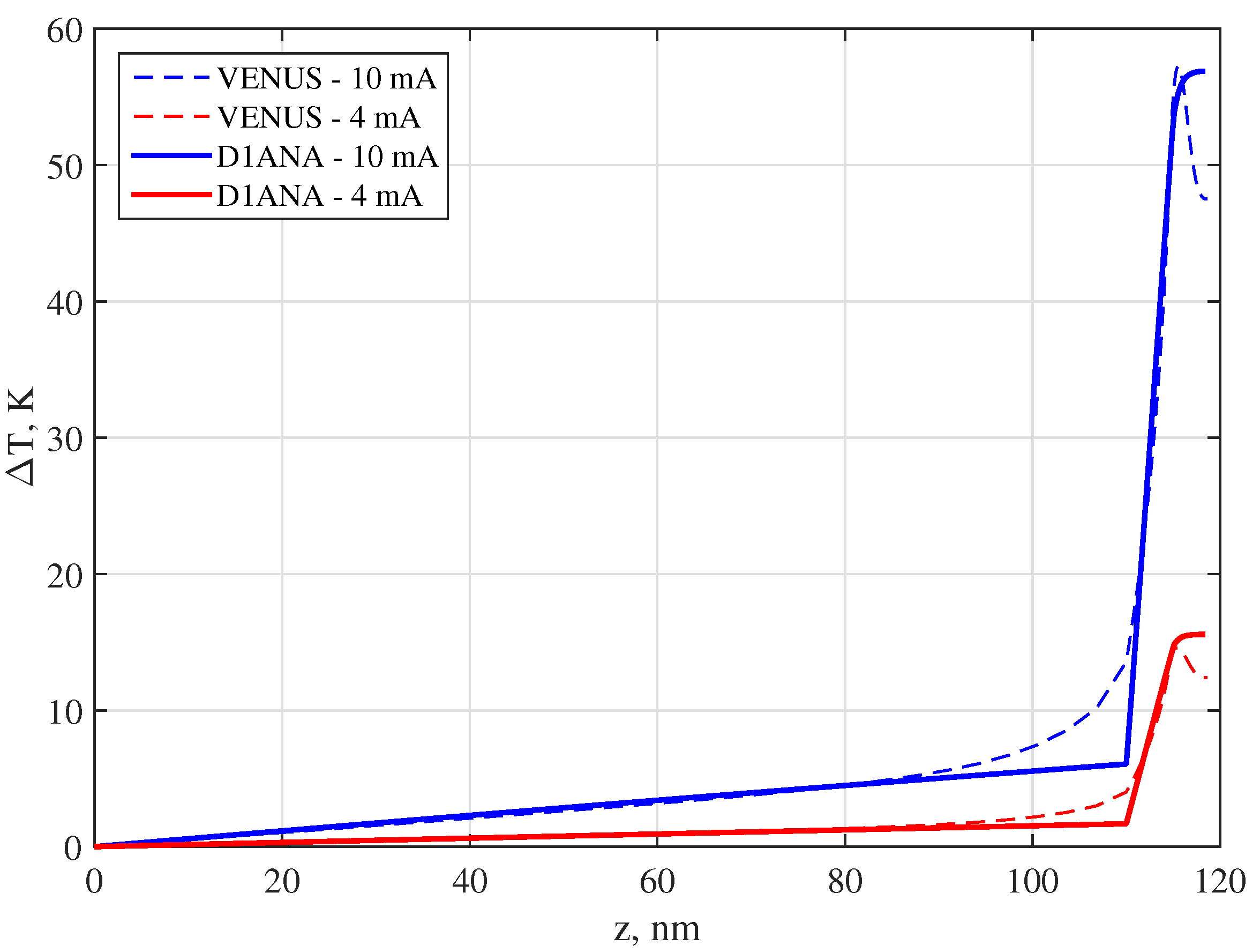
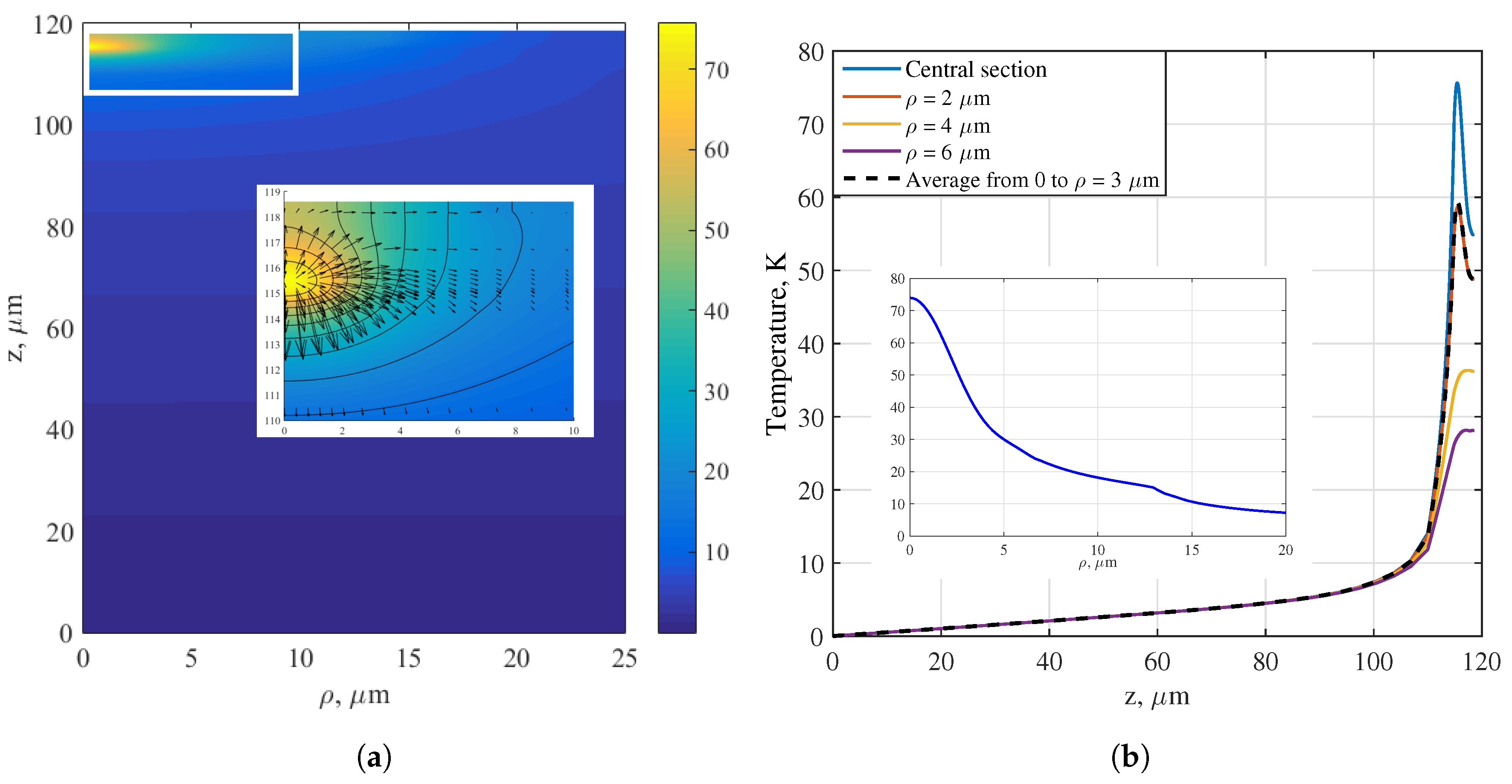
2.1. Thermal Problem

Heat is the main performance killer in VCSELs, the responsibility of power roll-over and of degradation at high ambient temperatures [21,47,48,49,50,51]. This can be grasped in Figure 2, where we mimic the effects of a pulsed operation regime by varying the duty cycle of the injected current. The heating not only shifts and quenches the optical gain spectrum (see Figure 3), but it also impacts on the current leakage, as shown in Figure 2b. As discussed in [10,11], while optical and electrical domains can be much reduced compared to actual device size (typically 150–250 μ m lateral size and 100–300 μ m height), the solution of the steady-state heat equation
· ( κ T ) = Q t o t
must include the full actual domain. In Equation (1), κ is the spatially-varying thermal conductivity and Q t o t is the sum of all the heat sources, which include Joule heating, free-carrier absorption, non-radiative recombinations, and QW capture heating.
Therefore, to stretch the actual thermal problem to a 1D longitudinal equation is the most challenging and demanding task in our investigation. To help the discussion, in Figure 4a we show the actual 3D thermal profile from VENUS. The heat sources (apart from Joule heating, which is not dominating) are focused in the MQW (multi-quantum well) region, i.e., a tiny part of the whole device, about 50 nm in longitudinal direction and 4 μ m in the radial direction, accounting for carrier lateral diffusion compared to the 2.35 μ m oxide aperture radius.
This has to be compared with the 12 times larger transverse size, which, in terms of area, means a factor of 144. This could be interpreted as a heat source filling factor of the thermal transverse domain. In a 1D perspective, Equation (1) loses azimuthal and radial dependence (shown as an inset of Figure 4b), and retains just the longitudinal variable z; the gradient operator reduces to a derivative along z.
Due to the much focused heat source, the temperature radial decay is strong at the MQW section, as shown by the different longitudinal cuts in Figure 4b (solid lines) and also by the black arrows in the inset of Figure 4a, representing the heat flow. Therefore we must carefully investigate and discuss how to treat such a major difference. As stated, the optical and electrical environments are mainly developing at the structure axis. The oxide aperture serves as both current and optical confinement. Therefore, carriers also nearly follow the oxide aperture size, allowing of course for some lateral spreading due to diffusion. Tightly connected to carriers is the gain profile, which is therefore also defined by the oxide aperture. The interaction with the optical gain of the guided modes and, in particular, of the fundamental mode (which is crucial, as most of the relevant sensing and datacom applications are aiming at single-mode operation) also completely occurs within the oxide aperture. Therefore, the temperature values relevant in VCSEL operation are those close to the axial region and we decided to make a surface average of the transverse temperature profile over the oxide area, which is shown in Figure 4b by the dashed black line.
In Figure 5, such average is reported for two currents, together with the achieved 1D fits. This was obtained by rescaling the temperature diffusion coefficients (corresponding to substrate and VCSEL) by factors that are related to the transverse filling factor of the heat source compared to the thermal domain.
In 1D this factor is 1 by definition, while in the actual case, it is in the order of hundreds. Therefore, we searched for equivalent 1D thermal conductivities that provided the best fit between the previously defined radial average of the 3D map and 1D longitudinal profiles. The much higher value achieved for the thermal conductivity of the substrate (a factor of 115) accounts for the very small filling factor discussed above. In addition, the thermal conductivity varies radially, especially in the mesa region where the filling factor is smaller (the passivation area almost does not contribute to heat conduction). This results in a much lower scaling factor of 2.5 in the VCSEL region. The 1D and 3D results fit nicely, especially in the most important section, the active region, and the major deviations are observed in the transition region between the substrate and the mesa. In that region, 3D effects make the transition smoother than in the 1D simulation, where a sharp slope change is observed. This is a consequence of the very large discontinuity in the values of thermal conductivities of the two thermal domains in the 1D limit. In any case, we verified that this difference does not appreciably affect optical and electrical characteristics.

2.2. Optical Problem

The only macroscopic observable quantity linked to temperature, although indirectly, is the emission wavelength [52], which varies during operation due to the temperature dependence of the semiconductor refractive index [53]. It can be linearized as follows:
n ( T ) = n ( T = 300   K ) + d n d T · ( T 300   K )
Such a change in refractive index modifies the resonance frequency of the optical resonator, as shown by Figure 6.
Together with the free carrier absorption, the temperature-dependent refractive index longitudinal profile causes the most important variation in the optical features during operation. In fact, the wavelength position determines the spectral position where the gain must be evaluated. Therefore, as shown in Figure 6, we have also carefully calibrated this parameter, so as to have a best fit with the experimental results. This requirement is easily explained by highlighting that the thermal profiles we are using are averages across the inner area (see Figure 4); however, the actual profile at the center, where the fundamental mode is also peaked, is higher, resulting in a stronger effect on the wavelength. Therefore, the lower temperature must be compensated by a larger coefficient to match the experimental results.

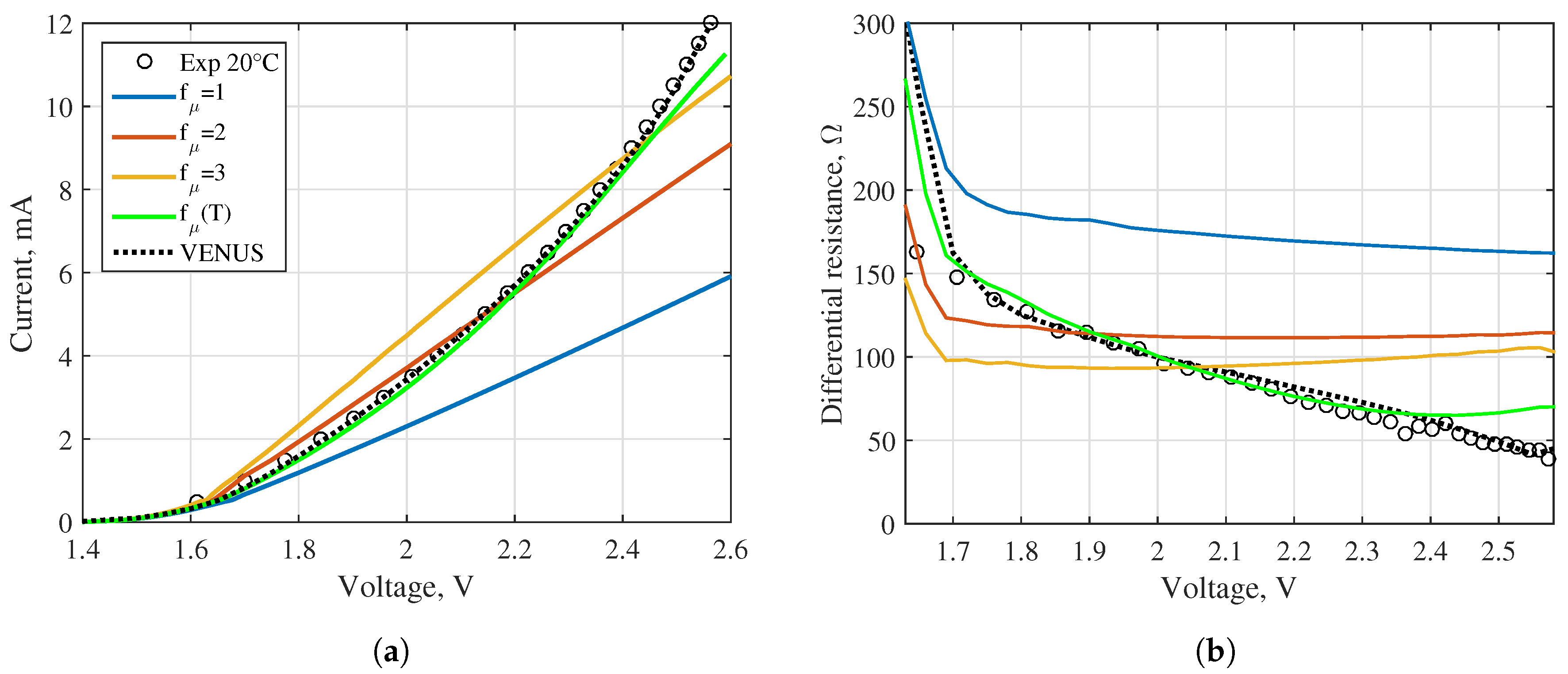
2.3. Electrical Problem
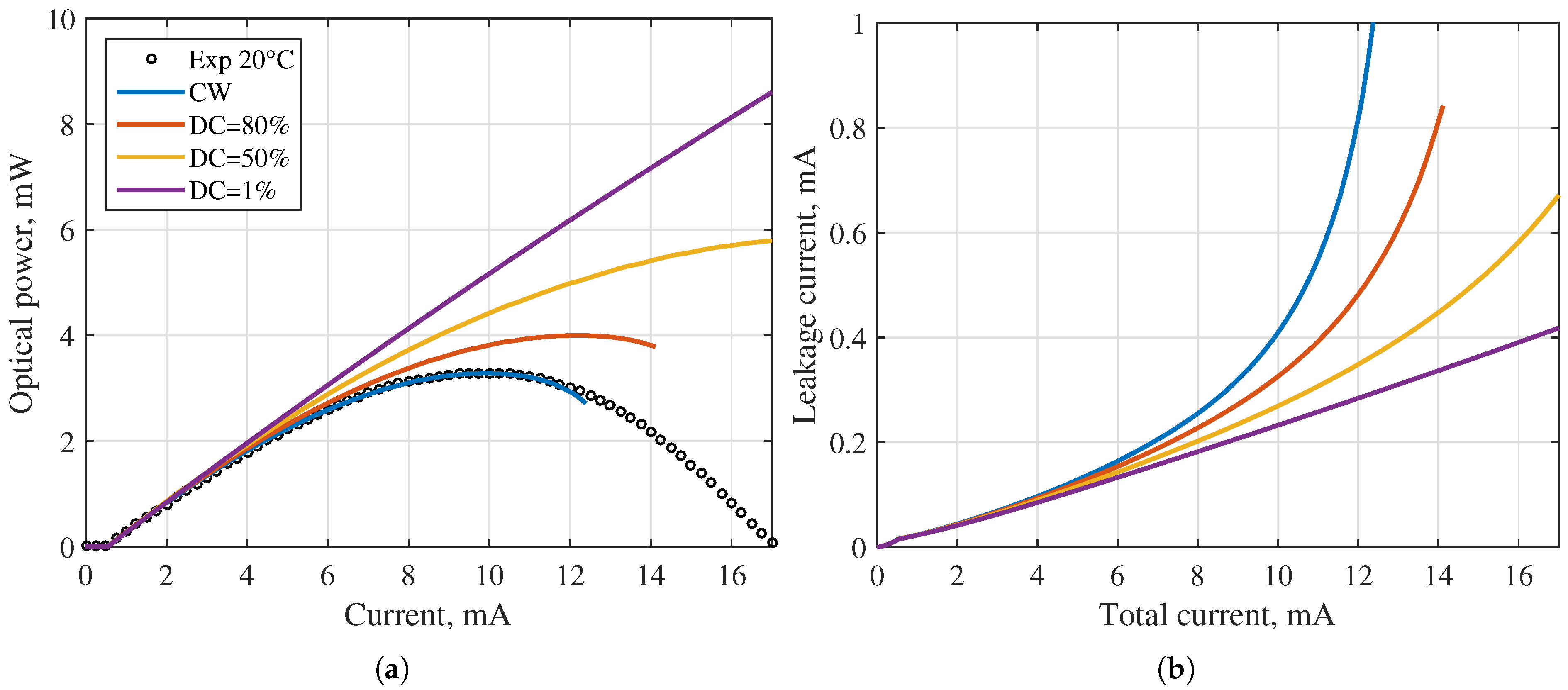
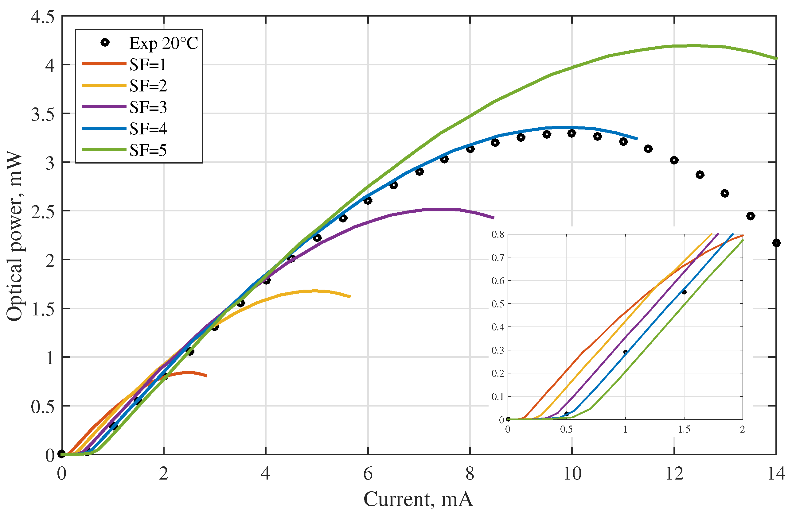
In this section we compare the electrical performance of the 1D model with the experimental results. In Figure 7, we vary the mobility [11] by a constant factor f μ . One can see that the relevant transverse effects discussed in our previous works [54] prevent, in this case, an agreement as good as with the previous quantities. Keeping the same VENUS mobility ( f μ = 1 ) results in resistivity that is too high. By increasing f μ , we get the same current as in the experimental results just for a certain voltage. Moreover, above the optical threshold, the differential resistance stays almost constant, as shown in Figure 7b, and it does not decrease as in the experimental results and in VENUS. To reproduce this behavior we suggest an operation-dependent f μ . The green line in Figure 7 shows the result of a linear variation on temperature of the kind:
f μ ( T ) = 1.2 + 3.5 × 10 2 · ( T 300   K )
This dependence quite satisfactorily fits the experimental data up to 10 mA, which is the range of interest in this work.

2.4. Optical Power

A very important difference between the 1D and the 3D model is the lack of absolute current and optical power values; in fact, a 1D model delivers only densities per unit area. The best way to find absolute values is to introduce an effective area [55], here assumed equal for optical power and current, to fit the L-I experimental curve. Using the oxide aperture as a reference area, in Figure 8 we show the effect of different size factors. A factor of 4 on the area (a factor of 2 in the radius) provides the best fit on both threshold (and also roll-over) current and maximum optical power.
For the electrical problem, this is best explained by current spreading and carrier diffusion [54,56]. For the optical problem, the larger area accounts for the larger transmission of a 3D mode compared to a 1D simulation (plane waves). In fact, as is well known, 3D optical threshold gain is always larger than in a 1D simulation.

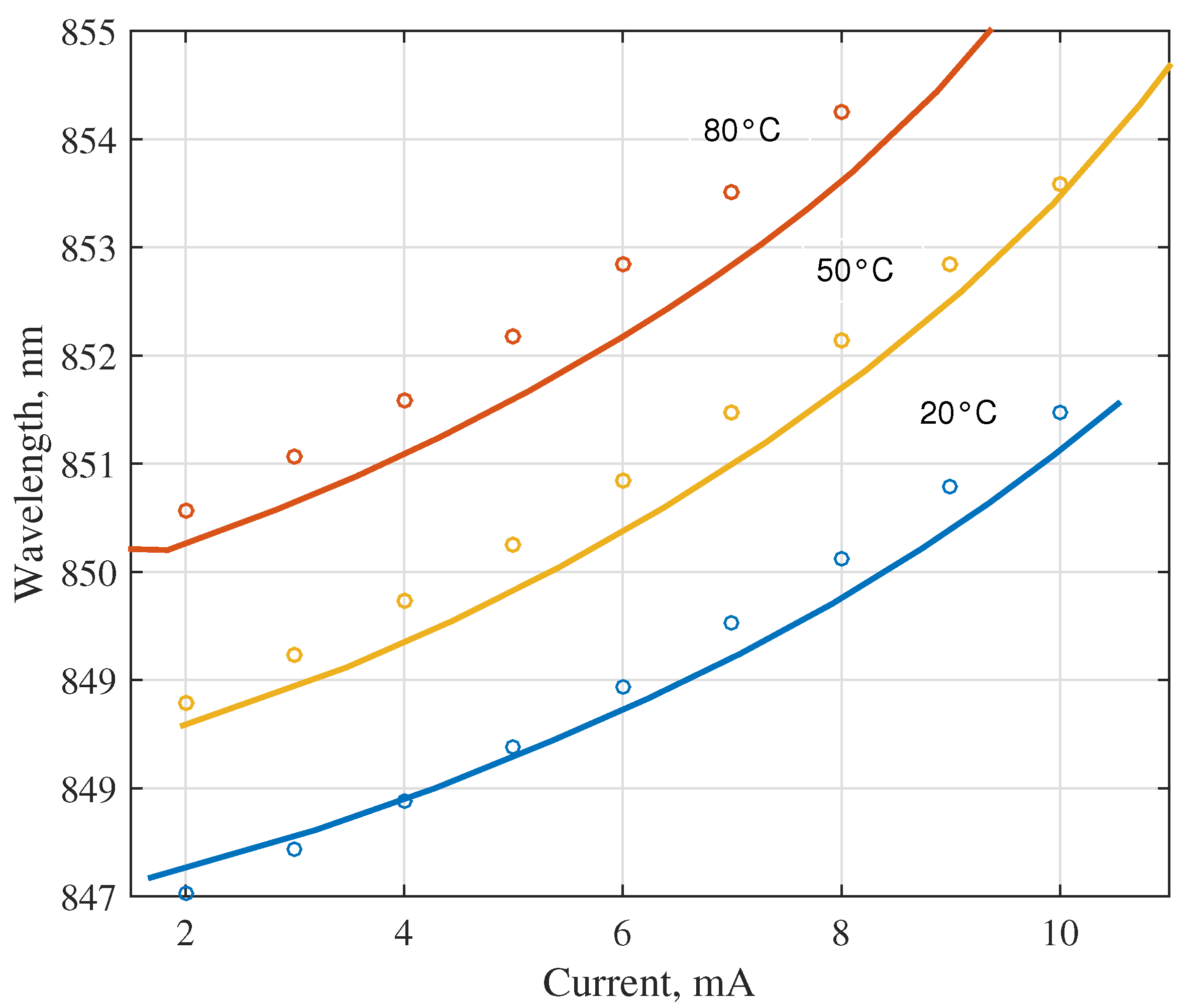
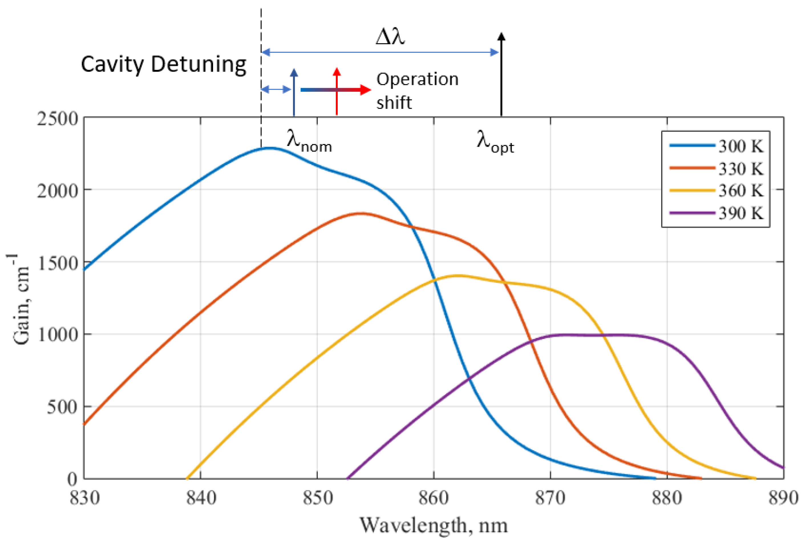
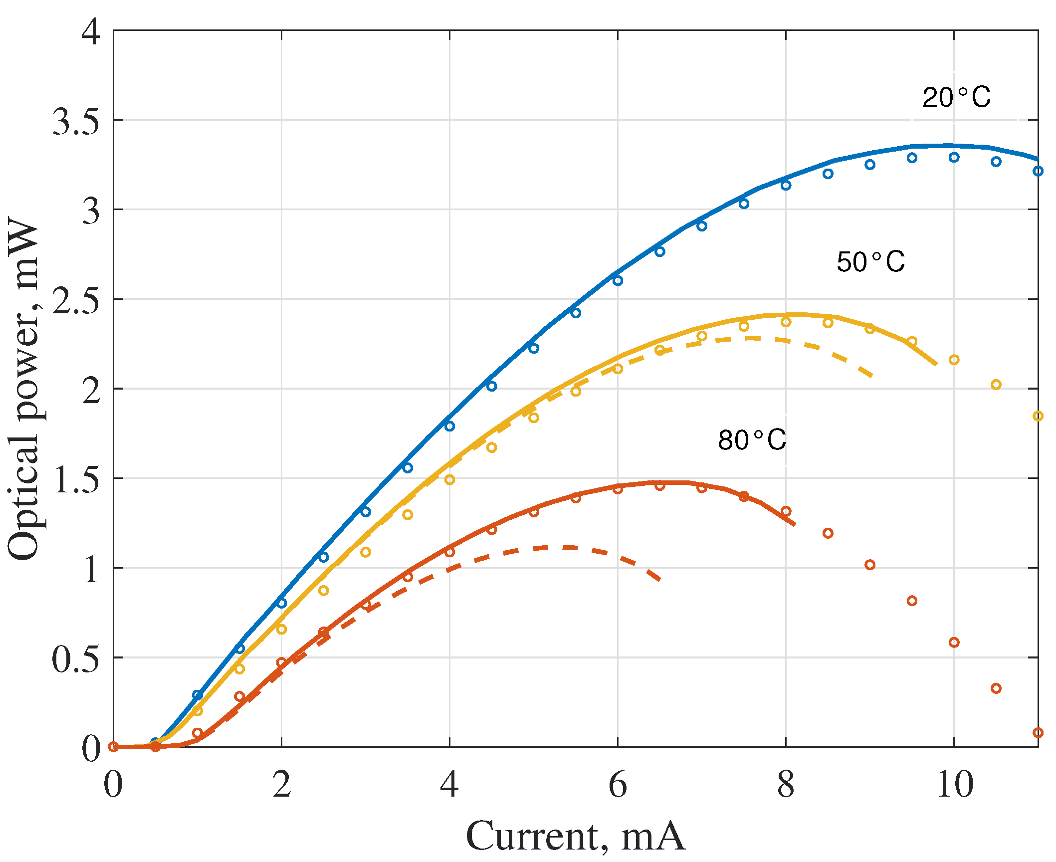
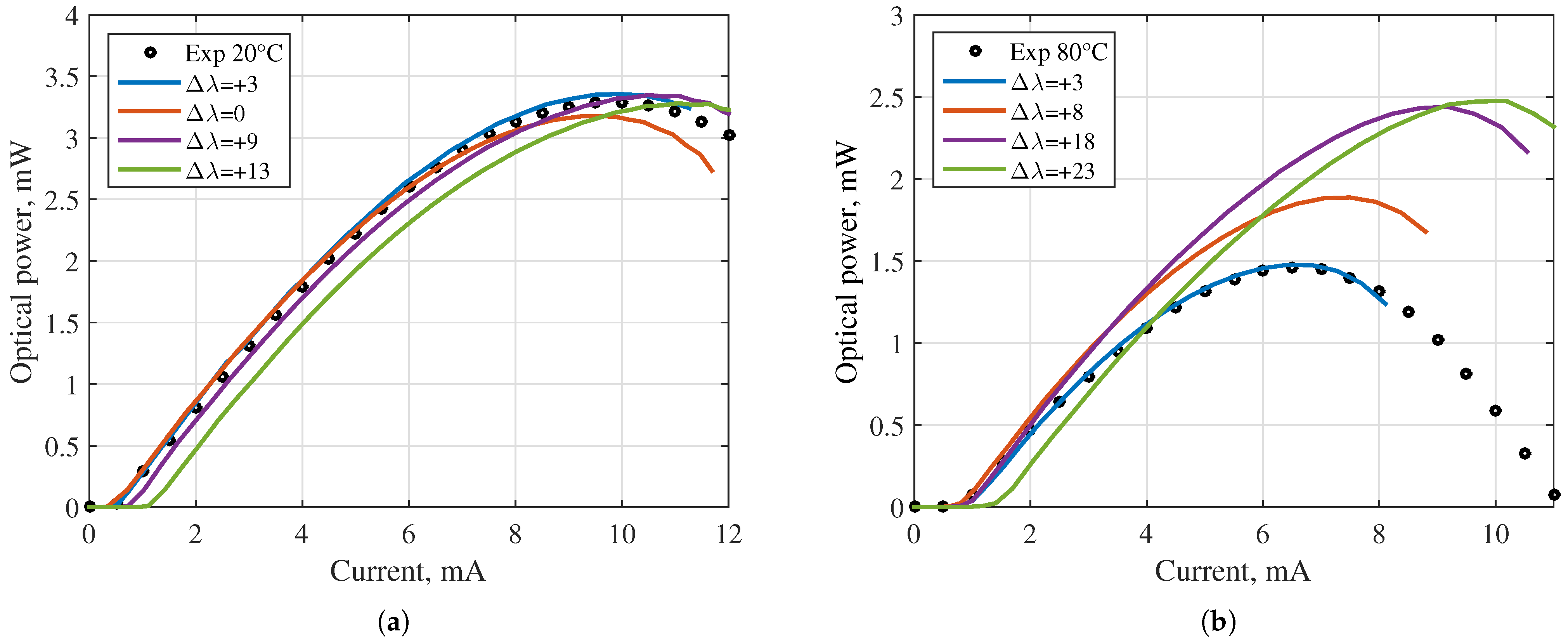
2.5. Optical Performance at High Ambient Temperatures

In view of improving performance at high ambient temperatures, we must take the last step of testing our calibrated D1ANA model in those operating conditions. This is performed in Figure 9, for three experimental ambient temperatures. It appears that a constant β T of 1.2 [11], which is excellent at room temperature, results in a temperature rise that is a little too high at higher ambient temperatures. We recall that this parameter rules the decrease of thermal conductivity with temperature, representing a nonlinear effect in the heat equation [57]:
κ = κ 300   K · T 300   K β T
Therefore, we varied β T so as to achieve a good fit between experimental and computed L-I at T a m b = 80 C. A good match is obtained for β T = 0.55 . For intermediate temperature values, we interpolate linearly, obtaining:
β T = 1.2 0.011 · ( T 293   K )

2.6. Parameter Alignment Summary

We have achieved good agreement for the L-I performance over a large ambient temperature range between our calibrated D1ANA suite and experimental results, as Figure 9 shows. This fitting procedure must be undertaken for every target device, and its steps are the ones discussed before. In summary, 5 parameters must be determined:
  • Rescaling of the thermal conductivities;
  • Rescaling of d n / d T ;
  • Rescaling of carrier mobility;
  • Finding an effective size;
  • Making β T temperature-dependent.
Once these parameters are found, D1ANA can be extensively applied at a much lower computational cost compared to VENUS. However, after this foundation work, the identification of the calibration parameter will be much faster.

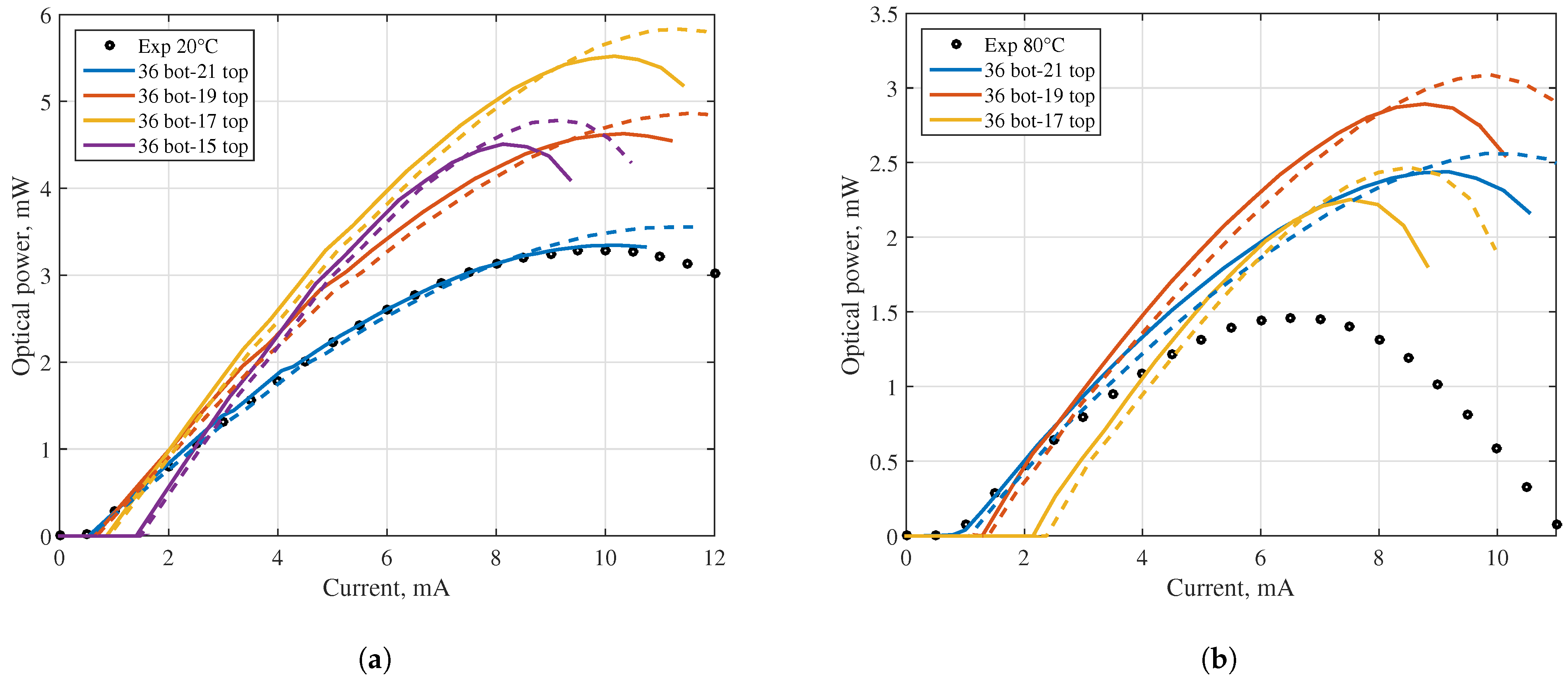
3. Examples of Application

We applied the calibrated D1ANA suite to investigate the cavity detuning ( Δ λ ) of this sample, in view of optimizing high-temperature operation, which is of crucial importance for VCSELs working in datacenters. The cavity detuning is defined as the wavelength difference between the maximum of the gain spectrum and the emission wavelength, as sketched in Figure 3.
This is a very important parameter for optimized operation, because the gain spectrum red-shifts much faster than the emission wavelength [58], by about a factor of four. For example, if one looks at Figure 6, the wavelength shifts by 4 nm for about a 60 K temperature increase inside the VCSEL. At the same increase, there corresponds a shift of the gain spectrum by 15 nm (blue and yellow gain spectra in Figure 3).
Figure 10a shows that the measured device is optimized for room-temperature operation, with a cavity detuning of +3 nm. At 80 C (Figure 10b) an 18 nm cavity detuning appears to be beneficial, since it would increase the maximum optical output power by 1 mW (from 1.5 to 2.5 mW), by almost leaving the threshold current unchanged. This can be understood from Figure 3, by comparing the different interactions between the optical line with the gain spectrum in the two cases of the nominal design ( λ n o m in Figure 3), and of the optimized one ( λ o p t ). A higher detuning would only increase the threshold current, leaving the maximum power about the same.
Another detail that strongly impacts on the output power and threshold current is the DBR radiation loss. The top-DBR radiation losses are “useful losses”, i.e., the optical output power (instead, the radiation in the substrate is lost). However, one must not think that the stronger the bottom-DBR reflection, the better. In fact, DBRs also induce absorption losses and, in addition, the bottom DBR is the main barrier for heat toward the heat-sink. This is due to the worse thermal conductivity to the ternary (AlGaAs) DBRs compared to the binary GaAs substrate, by a factor of 3.
In Figure 11, we study the effect of modifying the DBRs at the two ambient temperatures of 20 and 80 C. At room-temperature (Figure 11a), we find an improvement by reducing the number of output pairs to 4. At this value, we achieve 5.5 mW of maximum optical power, instead of the 3.3 mW of the nominal VCSEL. This occurs at 10 mA, the same current for which the experimental maximum power is detected at room temperature. From our simulations, a further reduction of the output DBR pairs causes an increase in the threshold current and the consequent higher heating in the device deteriorates the performance (violet curves), also in terms of maximum output power, which is reached at a lower current (8 mA). On the same plots, with dashed lines, we also report the case of a thinner bottom DBR, by 5 pairs, which corresponds to a VCSEL that is about 650 nm shorter. The results are fully in line with our previous comments. The thinner bottom DBR slightly increases the optical losses, and therefore the threshold slightly increases, and L-I curves are shifted to the right compared to the thicker mirror. However, the better thermal performance results in a later thermal rollover, allowing a marginal improvement of the maximum output power.
As shown in Figure 3, at high temperature the available gain more than halves, moving from 300 to 390 K at the same carrier density level, due to the larger broadening of the Fermi distributions. This is the main reason that eventually prevents VCSEL operation at a certain temperature. The lower gain must be compensated by a higher current density, which, in turn, is responsible for stronger recombinations. These are converted into heat, in a positive feedback loop that soon prevents lasing. Nonetheless, at 80 C, with a careful cavity detuning of Δ λ = + 18 nm (Figure 10b) and DBR optimization, we can nearly double the maximum output power, from 1.5 to 3 mW, at a current of 10 mA (Figure 11b). This is the same value that provides the maximum output power at room-temperature. The early rollover of the actual device at a higher temperature is due to its incorrect cavity detuning.

4. Conclusions and Outlook

In this paper, starting from good comparisons between experimental and simulation results, we have discussed the steps needed to dimensionally downscale our multiphysics 3D-suite VENUS. By identifying some crucial parameters and fitting them to the experimental results, we arrived at the calibrated D1ANA suite, which was shown to reproduce well the most interesting VCSEL features: I-V and L-I characteristics. In particular, the computed L-Is reproduce the experiments very well, in the ambient temperature range of 20–80 C, which covers the majority of possible applications.
As a result of dimensionality downscaling, D1ANA simulates VCSEL operation in about 80 s on an ordinary laptop (Intel Core i7-8550U, 1.80 GHz, Santa Clara, CA, USA), which is 35 times faster compared to VENUS, applying the same control parameters (voltage grid and convergence criteria for the Newton solver). Taking advantage of such an improved computational efficiency, we applied D1ANA to optimize the investigated device for high-temperature operation.
The calibrated D1ANA is a good compromise between a full multiphysics approach and the commonly used phenomenological models based on rate equations. Of course, we lose the optical transverse features. However, the much faster code is meant for a first rough identification of the parameter space to achieved given specs. Once that is identified by D1ANA, then VENUS can be applied for the last and finest details, among which are the modal features. Above all, these include the side-mode suppression ratio, in the case of typically desired single-mode operation.
We foresee other interesting applications of the calibrated D1ANA. For example, it could be used to test new injection schemes for next generation VCSELs; in particular, to switch from oxide-confined VCSELs to buried tunnel junction 850 nm devices [59]. A second potential purpose is its use to perform fast Monte-Carlo investigations of critical parameters, like cavity length, doping levels, and etching of the topmost GaAs contact layer. In fact, this requires a multispace parameter analysis that is not conceivable with VENUS. A third purpose is to extend D1ANA in the time domain, i.e., not looking for its stationary solution, but solving the dynamical system of equations. This would provide a new perspective from which to explore, for example, complex modulation schemes such as PAM4 (Pulse-amplitude modulation) or more complex ones, based on a nearly faithful multiphysics approach, which is unpractical with today’s computer power, using a 3D framework.

Author Contributions

Conceptualization, A.G. and P.D.; formal analysis, A.G. and P.D.; investigation, A.G. and P.D.; methodology, A.T., F.B. and P.D.; project administration, P.D.; software, A.G., A.T., F.B. and P.D.; supervision, M.G. and P.D.; visualization, A.G.; writing—original draft, A.G. and P.D.; writing—review and editing, A.T. and P.D. All authors have read and agreed to the published version of the manuscript.

Funding

This research received no external funding.

Institutional Review Board Statement

Not applicable.

Informed Consent Statement

Not applicable.

Data Availability Statement

No new data were created or analyzed in this study. Data sharing is not applicable to this article.

Conflicts of Interest

The authors declare no conflict of interest.

References

  1. Michalzik, R. (Ed.) VCSELs: Fundamentals, Technology and Applications of Vertical-Cavity Surface-Emitting Lasers; Springer: Berlin/Heidelberg, Germany, 2013. [Google Scholar] [CrossRef]
  2. Liu, A.; Wolf, P.; Lott, J.; Bimberg, D. Vertical-cavity surface-emitting lasers for data communication and sensing. Phys. Rev. 2019, 7, 121. [Google Scholar] [CrossRef]
  3. Moench, H.; Carpaij, M.; Gerlach, P.; Gronenborn, S.; Gudde, R.; Hellmig, J.; Kolb, J.; van der Lee, A. VCSEL based sensors for distance and velocity. Proc. SPIE 2016, 97660A-1-16. [Google Scholar] [CrossRef]
  4. Ebeling, K.J.; Michalzik, R.; Moench, H. Vertical-cavity surface-emitting laser technology applications with focus on sensors and three-dimensional imaging. Jpn. J. Appl. Phys. 2018, 52, 08PA02-1-11. [Google Scholar] [CrossRef]
  5. Dummer, M.; Johnson, K.; Rothwell, S.; Tatah, K.; Hibbs-Brenner, M. The role of VCSELs in 3D sensing and LiDAR. In Proceedings of the Optical Interconnects XXI. International Society for Optics and Photonics, Online Proceedings, 6–11 March 2021; Volume 11692, p. 116920C. [Google Scholar]
  6. Tatum, J.A.; Gazula, D.; Graham, L.A.; Guenter, J.K.; Johnson, R.H.; King, J.; Kocot, C.; Landry, G.D.; Lyubomirsky, I.; MacInnes, A.N.; et al. VCSEL-Based Interconnects for Current and Future Data Centers. J. Light. Technol. 2015, 33, 727–732. [Google Scholar] [CrossRef]
  7. Puerta, R.; Agustin, M.; Chorchos, L.; Tonski, J.; Kropp, J.R.; Ledentsov, N.; Shchukin, V.A.; Ledentsov, N.N.; Henker, R.; Monroy, I.T.; et al. 107.5 Gb/s 850 nm multi- and single-mode VCSEL transmission over 10 and 100 m of multi-mode fiber. In Proceedings of the 2016 Optical Fiber Communications Conference and Exhibition (OFC), Anaheim, CA, USA, 20–24 March 2016; pp. 1–3. [Google Scholar]
  8. Ledentsov, N., Jr.; Agustin, M.; Chorchos, L.; Ledentsov, N.N.; Turkiewicz, J.P. 25.78 Gbit/s data transmission over 2 km multi-mode-fibre with 850 and 910 nm single-mode VCSELs and a commercial quad small form-factor pluggable transceiver. Electron. Lett. 2018, 54, 774–775. [Google Scholar] [CrossRef]
  9. Kanakis, G.; Iliadis, N.; Soenen, W.; Moeneclaey, B.; Argyris, N.; Kalavrouziotis, D.; Spiga, S.; Bakopoulos, P.; Avramopoulos, H. High-Speed VCSEL-Based Transceiver for 200 GbE Short-Reach Intra-Datacenter Optical Interconnects. Appl. Sci. 2019, 9, 2488. [Google Scholar] [CrossRef] [Green Version]
  10. Tibaldi, A.; Bertazzi, F.; Goano, M.; Michalzik, R.; Debernardi, P. VENUS: A Vertical-cavity surface-emitting laser Electro-opto-thermal NUmerical Simulator. IEEE J. Select. Top. Quantum Electron. 2019, 25, 1500212. [Google Scholar] [CrossRef]
  11. Debernardi, P.; Tibaldi, A.; Daubenschüz, M.; Michalzik, R.; Goano, M.; Bertazzi, F. Probing thermal effects in VCSELs by experiment-driven multiphysics modeling. IEEE J. Select. Top. Quantum Electron. 2019, 25, 1700914. [Google Scholar] [CrossRef]
  12. Al-Samaneh, A.; Bou Sanayeh, M.; Miah, M.J.; Schwarz, W.; Wahl, D.; Kern, A.; Michalzik, R. Polarization-stable vertical-cavity surface-emitting lasers with inverted grating relief for use in microscale atomic clocks. Appl. Phys. Lett. 2012, 101, 171104. [Google Scholar] [CrossRef]
  13. Zhang, J.; Zhang, X.; Zhu, H.; Zhang, J.; Ning, Y.; Qin, L.; Wang, L. High-temperature operating 894.6nm-VCSELs with extremely low threshold for Cs-based chip scale atomic clocks. Opt. Express 2015, 23, 14763–14773. [Google Scholar] [CrossRef]
  14. Larsson, A.; Gustavsson, J.S.; Fülöp, A.; Haglund, E.; Haglund, E.P.; Kelkkanen, A. The Future of VCSELs: Dynamics and Speed Limitations. In Proceedings of the 2020 IEEE Photonics Conference (IPC), Vancouver, BC, Canada, 28 September–1 October 2020; pp. 1–2. [Google Scholar] [CrossRef]
  15. Westbergh, P.; Gustavsson, J.S.; Larsson, A. High Speed and High Temperature Operation of VCSELs. In Proceedings of the Optical Fiber Communication Conference. Optical Society of America, San Diego, CA, USA, 6–11 June 2015; p. M2D.5. [Google Scholar] [CrossRef]
  16. Hadley, G.R.; Lear, K.L.; Warren, M.E.; Choquette, K.D.; Scott, J.W.; Corzine, S.W. Comprehensive numerical modeling of vertical-cavity surface-emitting lasers. IEEE J. Quantum Electron. 1996, 32, 607–616. [Google Scholar] [CrossRef]
  17. Debernardi, P. HOT-VELM: A comprehensive and efficient code for fully vectorial and 3-D hot-cavity VCSEL simulation. IEEE J. Quantum Electron. 2009, 45, 979–992. [Google Scholar] [CrossRef]
  18. Gustavsson, J.S.; Vukusic, J.A.; Bengtsson, J.; Larsson, A. A comprehensive model for the modal dynamics of vertical-cavity surface-emitting lasers. IEEE J. Quantum Electron. 2002, 38, 203–212. [Google Scholar] [CrossRef]
  19. Nyakas, P.; Varga, G.; Puskás, Z.; Hashizume, N.; Kárpáti, T.; Veszprémi, T.; Zsombok, G. Self-consistent real three-dimensional simulation of vertical-cavity surface-emitting lasers. J. Opt. Soc. Am. B 2006, 23, 1761–1769. [Google Scholar] [CrossRef]
  20. Scott, J.W.; Geels, R.S.; Corzine, S.W.; Coldren, L.A. Modeling temperature effects and spatial hole burning to optimize vertical-cavity surface-emitting laser performance. IEEE J. Quantum Electron. 1993, 29, 1295–1308. [Google Scholar] [CrossRef]
  21. Mehta, K.; Liu, Y.S.; Wang, J.; Jeong, H.; Detchprohm, T.; Dupuis, R.D.; Yoder, P.D. Thermal Design Considerations for III-N Vertical-Cavity Surface-Emitting Lasers Using Electro-Opto-Thermal Numerical Simulations. IEEE J. Quantum Electron. 2019, 55, 1–8. [Google Scholar] [CrossRef]
  22. Sarzała, R.; Mendla, P.; Wasiak, M.; Maćkowiak, P.; Bugajski, M.; Nakwaski, W. Comprehensive self-consistent three-dimensional simulation of an operation of the GaAs-based oxide-confined 1.3-μm quantum-dot (InGa)As/GaAs vertical-cavity surface-emitting lasers. Opt. Quantum Electron. 2004, 36, 331–347. [Google Scholar] [CrossRef]
  23. Sarzała, R.P.; Śpiewak, P.; Nakwaski, W.; Wasiak, M. Cavity designs for nitride VCSELs with dielectric DBRs operating efficiently at different temperatures. Opt. Laser Technol. 2020, 132, 106482. [Google Scholar] [CrossRef]
  24. Calciati, M.; Tibaldi, A.; Bertazzi, F.; Goano, M.; Debernardi, P. Many-Valley Electron Transport in AlGaAs VCSELs. Semicond. Sci. Technol. 2017, 32, 055007. [Google Scholar] [CrossRef]
  25. Coldren, L.A.; Corzine, S.W. Diode Lasers and Photonic Integrated Circuits; John Wiley & Sons: New York, NY, USA, 1995. [Google Scholar]
  26. Streiff, M.; Witzig, A.; Pfeiffer, M.; Royo, P.; Fichtner, W. A comprehensive VCSEL device simulator. IEEE J. Select. Top. Quantum Electron. 2003, 9, 879–891. [Google Scholar] [CrossRef]
  27. Mehta, K.; Liu, Y.S.; Wang, J.; Jeong, H.; Detchprohm, T.; Park, Y.J.; Alugubelli, S.R.; Wang, S.; Ponce, F.A.; Shen, S.C.; et al. Lateral Current Spreading in III-N Ultraviolet Vertical-Cavity Surface-Emitting Lasers Using Modulation-Doped Short Period Superlattices. IEEE J. Quantum Electron. 2018, 54, 2400507. [Google Scholar] [CrossRef]
  28. Debernardi, P.; Orta, R. Analytical Electromagnetic Solution for Bragg Mirrors With Graded Interfaces and Guidelines for Enhanced Reflectivity. IEEE J. Quantum Electron. 2007, 43, 269–274. [Google Scholar] [CrossRef]
  29. Schubert, E.F.; Tu, L.W.; Zydzik, G.J.; Kopf, R.F.; Benvenuti, A.; Pinto, M.R. Elimination of heterojunction band discontinuities by modulation doping. Appl. Phys. Lett. 1992, 60, 466–468. [Google Scholar] [CrossRef] [Green Version]
  30. Bertazzi, F.; Goano, M.; Ghione, G.; Tibaldi, A.; Debernardi, P.; Bellotti, E. Electron Transport. In Handbook of Optoelectronic Device Modeling and Simulation; Piprek, J., Ed.; CRC Press: Boca Raton, FL, USA, 2017; Chapter 2; pp. 35–80. [Google Scholar] [CrossRef]
  31. De Falco, C.; Gatti, E.; Lacaita, A.L.; Sacco, R. Quantum-corrected drift-diffusion models for transport in semiconductor devices. J. Comp. Phys. 2005, 204, 533–561. [Google Scholar] [CrossRef]
  32. Cédola, A.P.; Kim, D.; Tibaldi, A.; Tang, M.; Khalili, A.; Wu, J.; Liu, H.; Cappelluti, F. Physics-based modeling and experimental study of Si-doped InAs/GaAs quantum dot solar cells. Int. J. Photoenergy 2018, 2018, 7215843-1-10. [Google Scholar] [CrossRef]
  33. Goano, M. Series Expansion of the Fermi-Dirac Integral Fj(x) over the Entire Domain of Real j and x. Solid-State Electron. 1993, 36, 217–221. [Google Scholar] [CrossRef]
  34. Goano, M. Algorithm 745. Computation of the complete and incomplete Fermi-Dirac integral. ACM Trans. Math. Softw. 1995, 21, 221–232. [Google Scholar] [CrossRef]
  35. De Santi, C.; Meneghini, M.; Tibaldi, A.; Vallone, M.; Goano, M.; Bertazzi, F.; Verzellesi, G.; Meneghesso, G.; Zanoni, E. Physical mechanisms limiting the performance and the reliability of GaN-based LEDs. In Nitride Semiconductor Light-Emitting Diodes, 2nd ed.; Huang, J.J., Kuo, H.C., Shen, S.C., Eds.; Woodhead Publishing: Duxford, UK, 2018; Chapter 14; pp. 455–489. [Google Scholar] [CrossRef]
  36. Lades, M.; Kaindl, W.; Kaminski, N.; Niemann, E.; Wachutka, G. Dynamics and incomplete ionized dopants and their impact on 4H/6H–SiC devices. IEEE Trans. Electron Devices 1999, 46, 598–604. [Google Scholar] [CrossRef]
  37. Heilman, R.; Oelgart, G. Ionization energy of the carbon acceptor in AlxGa1−xAs. Semicond. Sci. Technol. 2015, 5, 1040–1045. [Google Scholar] [CrossRef]
  38. Grupen, M.; Hess, K. Simulation of carrier transport and nonlinearities in quantum-well laser diodes. IEEE J. Quantum Electron. 1998, 34, 120–140. [Google Scholar] [CrossRef]
  39. Witzigmann, B.; Witzig, A.; Fichtner, W. A multidimensional laser simulator for edge-emitters including quantum carrier capture. IEEE Trans. Electron Devices 2000, 47, 1926–1934. [Google Scholar] [CrossRef]
  40. Hybertsen, M.S.; Witzigmann, B.; Alam, M.A.; Smith, R.K. Role of carrier capture in microscopic simulation of multi-quantum-well semiconductor laser diodes. J. Comp. Electron. 2002, 1, 113–118. [Google Scholar] [CrossRef]
  41. Baraff, G.A. Semiclassical description of electron transport in semiconductor quantum-well devices. Phys. Rev. B 1997, 55, 10745–10753. [Google Scholar] [CrossRef]
  42. Tessler, N.; Eisenstein, G. On Carrier Injection and Gain Dynamics in Quantum Well Lasers. IEEE J. Quantum Electron. 1993, QE-29, 1586–1595. [Google Scholar] [CrossRef]
  43. Bava, G.P.; Debernardi, P.; Fratta, L. Three-dimensional model for vectorial fields in vertical-cavity surface-emitting lasers. Phys. Rev. A 2001, 63, 23816. [Google Scholar] [CrossRef]
  44. Debernardi, P.; Bava, G.P. Coupled mode theory: A powerful tool for analyzing complex VCSELs and designing advanced devices features. IEEE J. Select. Top. Quantum Electron. 2003, 9, 905–917. [Google Scholar] [CrossRef]
  45. Debernardi, P.; Simaz, A.; Tibaldi, A.; Boisnard, B.; Camps, T.; Bertazzi, F.; Goano, M.; Reig, B.; Doucet, J.B.; Bardinal, V. Anisotropic Transverse Confinement Design for Electrically Pumped 850 nm VCSELs Tuned by an Intra Cavity Liquid-Crystal Cell. IEEE J. Select. Top. Quantum Electron. 2021. [Google Scholar] [CrossRef]
  46. Chuang, S. Physics of Photonic Devices, 2nd ed.; Wiley: Hoboken, NJ, USA, 2009. [Google Scholar]
  47. Weigl, B.; Grabherr, M.; Jung, C.; Jager, R.; Reiner, G.; Michalzik, R.; Sowada, D.; Ebeling, K. High-performance oxide-confined GaAs VCSELs. IEEE J. Sel. Top. Quantum Electron. 1997, 3, 409–415. [Google Scholar] [CrossRef]
  48. Baveja, P.P.; Kögel, B.; Westbergh, P.; Gustavsson, J.S.; Haglund, Å.; Maywar, D.N.; Agrawal, G.P.; Larsson, A. Assessment of VCSEL thermal rollover mechanisms from measurements and empirical modeling. Opt. Express 2011, 19, 15490–15505. [Google Scholar] [CrossRef]
  49. Bertazzi, F.; Goano, M.; Bellotti, E. Calculation of Auger lifetime in HgCdTe. J. Electron. Mater. 2011, 40, 1663–1667. [Google Scholar] [CrossRef]
  50. Calciati, M.; Goano, M.; Bertazzi, F.; Vallone, M.; Zhou, X.; Ghione, G.; Meneghini, M.; Meneghesso, G.; Zanoni, E.; Bellotti, E.; et al. Correlating electroluminescence characterization and physics-based models of InGaN/GaN LEDs: Pitfalls and open issues. AIP Adv. 2014, 4, 067118. [Google Scholar] [CrossRef]
  51. Piprek, J. What Limits the Efficiency of High-Power InGaN/GaN Lasers? IEEE J. Quantum Electron. 2017, 53, 1–4. [Google Scholar] [CrossRef]
  52. Farzaneh, M.; Amatya, R.; Lüerßen, D.; Greenberg, K.J.; Rockwell, W.E.; Hudgings, J.A. Temperature profiling of VCSELs by thermoreflectance microscopy. IEEE Photon. Technol. Lett. 2007, 19, 601–603. [Google Scholar] [CrossRef]
  53. Gehrsitz, S.; Reinhart, F.K.; Gourgon, C.; Herres, N.; Vonlanthen, A.; Sigg, H. The refractive index of AlxGa1−xAs below the band gap: Accurate determination and empirical modeling. J. Appl. Phys. 2000, 87, 7825–7837. [Google Scholar] [CrossRef]
  54. Tibaldi, A.; Gonzalez Montoya, J.A.; Bertazzi, F.; Goano, M.; Daubenschüz, M.; Michalzik, R.; Debernardi, P. Bridging scales in multiphysics VCSEL modeling. Opt. Quantum Electron. 2019, 51, 231. [Google Scholar] [CrossRef]
  55. Gullino, A.; Tibaldi, A.; Bertazzi, F.; Goano, M.; Daubenschüz, M.; Michalzik, R.; Debernardi, P. Modulation response of VCSELs: A physics-based simulation approach. In Proceedings of the 20th International Conference on Numerical Simulation of Optoelectronic Devices (NUSOD 2020), Turin, Italy, 14–25 September 2020; pp. 65–66. [Google Scholar] [CrossRef]
  56. Kalosha, V.P.; Shchukin, V.A.; Ledentsov, N.; Ledentsov, N.N. Comprehensive Analysis of Electric Properties of Oxide-Confined Vertical-Cavity Surface-Emitting Lasers. IEEE J. Sel. Top. Quantum Electron. 2019, 25, 1–9. [Google Scholar] [CrossRef]
  57. Adachi, S. (Ed.) Properties of Aluminium Gallium Arsenide; EMIS Datareviews Series; INSPEC: London, UK, 1993. [Google Scholar]
  58. Tell, B.; Brown-Goebeler, K.; Leibenguth, R.; Baez, F.; Lee, Y.H. Temperature dependence of GaAs-AlGaAs vertical cavity surface emitting lasers. Appl. Phys. Lett. 1992, 60, 683–685. [Google Scholar] [CrossRef]
  59. Tibaldi, A.; Gonzalez Montoya, J.A.; Alasio, M.G.C.; Gullino, A.; Larsson, A.; Debernardi, P.; Goano, M.; Vallone, M.; Ghione, G.; Bellotti, E.; et al. Analysis of carrier transport in tunnel-junction vertical-cavity surface-emitting lasers by a coupled nonequilibrium Green’s function–drift-diffusion approach. Phys. Rev. Appl. 2020, 14, 024037. [Google Scholar] [CrossRef]
Figure 1. Schematics of 3D structure investigated in VENUS and 1D structure simulated in D1ANA, where only a longitudinal direction z problem is solved.
Applsci 11 06908 g001
Figure 2. Effect of the heating in VCSEL operation (CW—continuous wave; DC—duty cycle) at 20 C. The impact of reduced internal heating is parametrically investigated for the output power (a) and leakage current (b) on our test device.
Applsci 11 06908 g002
Figure 3. Gain spectra at different ambient temperatures, with electron and hole sheet densities set at 4 × 10 12 cm 2 . The concept of cavity detuning is sketched at the top of the figure. λ n o m refers to actual VCSEL design ( Δ λ = 3 nm), λ o p t to larger detuning values.
Applsci 11 06908 g003
Figure 4. Temperature features of the reference device, at T a m b = 20 C and injected current of 10 mA, corresponding to the maximum optical power of about 3.3 mW. (a) Temperature map on the “electrical domain”, set as half of the thermal one. In the inset: a zoom of the VCSEL region (DBRs + cavity), with contour lines at 5 C steps and arrows indicating heat flow. (b) Temperature profiles cut at different radii (solid lines) and oxide aperture averaged temperature profile (black dotted line). The inset shows the radial temperature variation in the central QW.
Applsci 11 06908 g004
Figure 5. Dashed lines: oxide aperture averaged 3D temperature longitudinal cuts at 4 and 10 mA. Continuous lines: 1D approximation by rescaling the thermal conductivities by a factor of 115 for the substrate and 2.5 in the VCSEL region (DBRs + cavity). The original values [11] are 0.46 W/mK (substrate) and 0.15 W/m K (DBRs and cavity).
Applsci 11 06908 g005
Figure 6. Wavelength red-shift vs. current, for different ambient temperatures (20, 50, 80 C). Experimental values (open circles) are compared to 1D computed values (continuous lines).
Applsci 11 06908 g006
Figure 7. (a) Experimental and VENUS current voltage (I-V) characteristics ( T a m b = 20 C) compared with the 1D model, with mobility factors that modify the 3D values. (b) Corresponding differential resistances compared with VENUS and experimental result.
Applsci 11 06908 g007
Figure 8. Experimental light-current (L-I) characteristics ( T a m b = 20 C) compared with the 1D model, with different size factors (SF). The inset shows the threshold behavior.
Applsci 11 06908 g008
Figure 9. L-I characteristics at three different ambient temperatures (20, 50, 80 °C). Open circles refer to experimental results, solid lines to the proposed calibrated 1D model, Equation (5), and dashed lines to a constant β T = 1.2 .
Applsci 11 06908 g009
Figure 10. L-I characteristics at different cavity detuning values at 20 (a) and 80 °C (b).
Applsci 11 06908 g010
Figure 11. L-I characteristics for two ambient temperatures: (a) 20 C; (b) 80 C, with different combinations of top and bottom DBR pairs; dashed lines refer to a 31-pair bottom DBR. In the DBR optimization at 80 C, a cavity detuning of Δ λ = + 18 nm is used (see Figure 10b).
Applsci 11 06908 g011
Publisher’s Note: MDPI stays neutral with regard to jurisdictional claims in published maps and institutional affiliations.

