1. Introduction
Novel empty devices based on coaxial transmission lines have been studied in recent years due to their interesting properties: pure-TEM propagation, non-dispersion, low radiation, low loss and high Q (unloaded quality factor), among others. This good performance can be achieved, essentially, due to the absence of dielectric, which reduces the degradation of electromagnetic waves and allows operation at a very high frequency without severe deterioration. Nevertheless, difficult manufacturing processes, high cost or difficult integration with other planar systems are inherent problems to topologies based on coaxial lines [
1].
One possibility to solve the aforementioned drawbacks is the use of empty cavities in multilayer printed circuit boards (PCBs) to provide enhanced, integrated, and self-packaged substrate integrated devices, which is a research area that is attracting much interest in recent years.
One of the most popular alternatives to implement this kind of integrated circuit is substrate integrated suspended line (SISL) [
2]. In this technology, a layer of dielectric is used to support a metallic strip. This main layer is enclosed by other layers, below and above it, that are emptied around the strip. Finally, the structure is closed with the top and bottom layers that are not emptied, and therefore they isolate the main strip from the outside. This structure forms a completely integrated enclosing for the main line, which, being almost empty, provides better propagation performance than traditional dielectric-filled planar lines. It is also easy to fabricate and is low cost. Because of its good characteristics, many devices have been implemented using SISL. For example, only in the last year, the literature has offered designs of filters [
3,
4], antennas [
5,
6], or couplers and power dividers [
7,
8], among others.
Another popular alternative to provide an empty substrate integrated transmission line is empty substrate integrated coaxial line (ESICL), first presented in [
9] and later developed in [
10]. ESICL is a structure that can be entirely fabricated with the standard dielectric substrate layers by using exclusively printed circuit board (PCB) standard manufacturing procedures. ESICL is built up by piling five conventional substrate layers, conveniently emptied where necessary, which create a metallic cavity in which a rectangular coaxial conductor is suspended. In comparison with SISL, which is only partially emptied, i.e., a dielectric substrate is used to support the main strip, ESICL provides a completely empty and integrated coaxial-like line, which performs even better than SISL, since guided waves do not interact with a lossy dielectric inside ESICL. In addition, ESICL is a pure TEM line (not quasi-TEM like microstrip or SISL), which is also an important advantage. Devices implemented in ESICL, like filters [
10,
11], inverters [
12], power dividers or directional couplers [
13], can be manufactured quite easily and would achieve very high-quality responses and low losses, with performance much better than devices integrated in conventional planar lines or substrate integrated circuits (SICs), such as substrate integrated waveguide (SIW) [
1], and only comparable to other completely emptied integrated waveguides, which is the case of the empty substrate integrated waveguide (ESIW) [
1].
Two types of transitions are now currently available to inject power from conventional feeding lines to the ESICL structure: a grounded co-planar waveguide to ESICL (GCPW-ESICL) [
10] and a microstrip-ESICL [
14]. Both transitions feed the ESICL by the central layer and require a covered pseudo-transformer with a combination of metallized and non-metallized parts; this transformer is the most complicated element, requiring an accurate design and is relatively large.
In this work, a new transition is presented that feeds the ESICL structure from the top cover with a through-wire connecting the microstrip line with the inner coaxial conductor. The benefits of this transition are its compactness, its simplicity, the possibility of having different layer heights for the feeding layer and the ESICL device and the possibility for the feeding line to adopt any angle of orientation within the plane of the top cover. All aforementioned advantages are important, but among them stands out the possibility of using an arbitrary angle between the feeding line and ESICL, and the use of different layers to implement planar lines and ESICL. The main application of a transition such as the one proposed in this paper is providing a means to develop hybrid planar/ESICL circuits, where the strengths of both technologies can be exploited. This main application is clearly reinforced by the main identified advantages. On the one hand, a transition showing a strong independence with the feeding angle provides flexibility to distribute the different circuits or elements in the available space. On the other hand, having ESICL and planar lines in different layers allows to overlap both technologies, achieving higher degrees of compactness and providing even more flexibility to the development of hybrid planar/ESICL circuits.
This paper is organized as follows:
Section 2 deals with the design of the transition, whereas the results of a back-to-back prototype are presented in
Section 3; finally, main conclusions are discussed in
Section 4.
2. Design of the Transition
This through-wire microstrip-to-ESICL transition is inspired in the classical coaxial-to-waveguide transition [
15] and in the equivalent through-wire transition for ESIW [
16]. In the classical transition, the coaxial line is used as the feeding line to excite a waveguide; it presents a lot of practical performances [
17], however, the coaxial probe is never connected to the walls of the waveguide. On the other hand, in the case of the transition to ESIW, the through-wire connects the feeding microstrip line with the bottom layer of the ESIW, achieving impedance matching with a transformer and a pad-gap structure located in the top layer of the ESIW. This new through-wire approach to ESICL presents a smart solution to directly connect a microstrip feeding line with the inner coaxial conductor of the ESICL; as the microstrip and ESICL are designed to have the same impedance, no intermediate transformer is required, only a pad-gap structure is necessary for the through-wire. Consequently, the design procedure is simpler than the former cases and the number of parameters that control the transition are fewer. The proposed structure for the through-wire microstrip-to-ESICL is that shown in
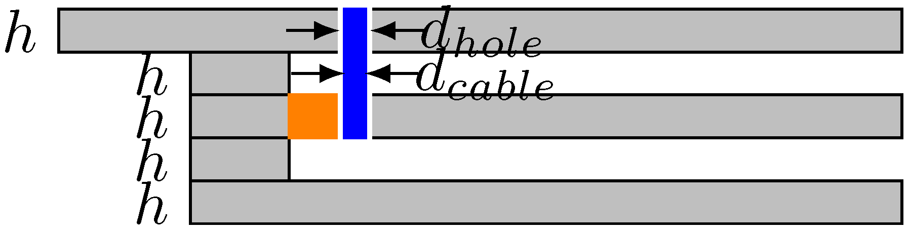
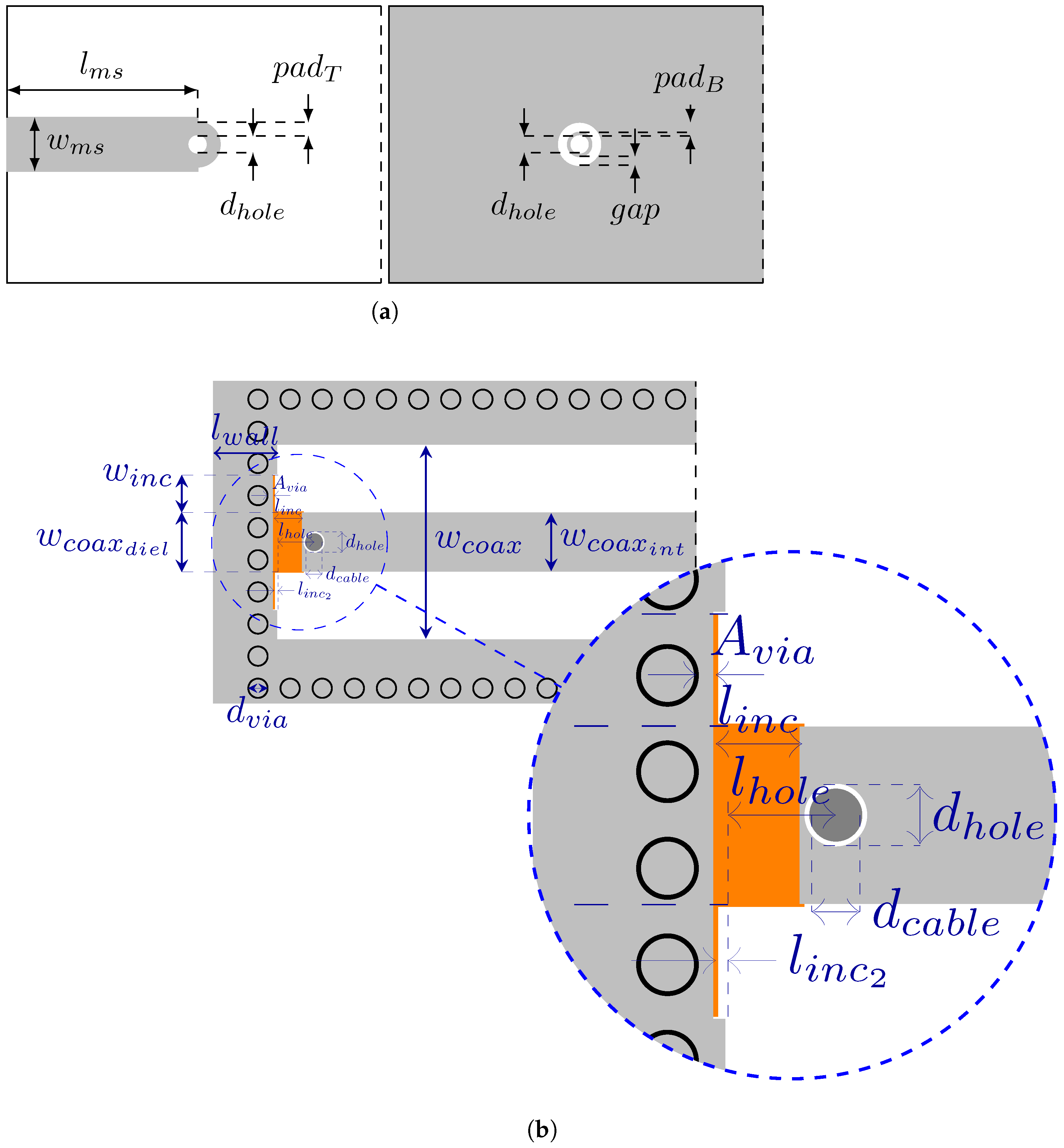
Figure 1. The detailed layout of the top and central layers is depicted in
Figure 2.
As it can be observed, the feeding microstrip and the inner coaxial lines are totally independent and located in different layers. To transfer power to the ESICL structure, a metallic filament is used to electrically connect the microstrip feeding line with the base of the inner coaxial line. The filament is tin soldered to the top and central layers. To avoid short circuiting the microstrip with its ground by the bottom side of the top cover (which is also the ground of the ESICL), the filament of diameter
, uses a pad-gap structure, controlled by the parameters
,
and
(see
Figure 2a). On the other hand, the filament requires a hole of diameter
in the inner coaxial to be inserted. Three important details can be noticed in this transition: the first one is that the inner coaxial is totally isolated from its ground (see details in
Figure 2b), for which the non-metallic section controlled by the parameter
is used (
is just used to ease the manufacturing); via holes are non-necessary in the inner coaxial to ensure the confinement of the electromagnetic field as it happens in previous transitions. The second detail is that no transformation is required in the feeding line, as the initial microstrip directly feeds the through-wire transition, given that the impedance of both the microstrip and inner coaxial line is the same. Finally, the third detail is that, given its circular symmetry, this transition is almost insensitive to the rotation of the microstrip around the filament, as it is proved in [
16].
The procedure to design this transition, in the band of interest from 0 to 20 GHz, is as follows. The initial step adjusts the width of the lines,
for microstrip and
,
for ESICL, so that both lines have the same impedance of 50
at the central frequency of interest (
= 10 GHz). Then, the initial values for the through-wire transition (
,
,
,
) are set according to the procedure stated in [
16], where
is rounded to the nearest available commercial diameter and
. The rest of the parameters are set following [
10], with the exception of
and
, whose values do not affect the structure and are arbitrarily set to ease the manufacturing.
A performance study (transmission and reflection coefficients of the transition) was carried out to analyze which parameters have the biggest influence apart from those controlling the pad-gap structure and the isolation of the coaxial. As the cable diameter is smaller, the response is better; then = 0.5 mm is chosen, given that it is the smallest commercial filament that can be easily manipulated and soldered. The position of the filament in the inner coaxial is also sensitive, the response being improved as it is closer to the beginning of the coaxial line; then, just a tiny guard margin of 0.05 mm is included in to ensure the soldering of the filament within the coaxial. After that, just four dimensions are critical to adjust the transition (, , , ), which are optimized with a Nelder–Mead simplex algorithm in CST Studio Suite 2019 to maximize the return losses in the band of interest.
3. Results
As losses in this transition are mainly due to the presence of the dielectric, they could be reduced if substrates with an adequate loss behavior were used. Two ESICL back-to-back prototypes in the band 0–20 GHz were designed to validate this through-wire transition and its design procedure. For the first transition, a Taconic RF-10 substrate of permitivity
= 10.2, 0.25 mm height and copper metallization of 17.5
m with an additional copper electrodeposition of 9
m has been used to manufacture the microstrips, and it has been used a Rogers 4003C substrate of permitivity
= 3.55, 0.813 mm height and copper metallization of 17.5
m (plus 9
m of electrodeposition) for the rest of the layers.
Table 1 shows the final dimensions for the first transition after the optimization process, whereas simulated results can be seen in
Figure 3.
For the second version of the transition, the same Rogers 4003C (0.813 mm height and 26.5
m of total metallization) substrate was used for all the layers.
Table 2 shows the final dimensions for the second transition (all the layers manufactured with Rogers 4003C) after the optimization process.
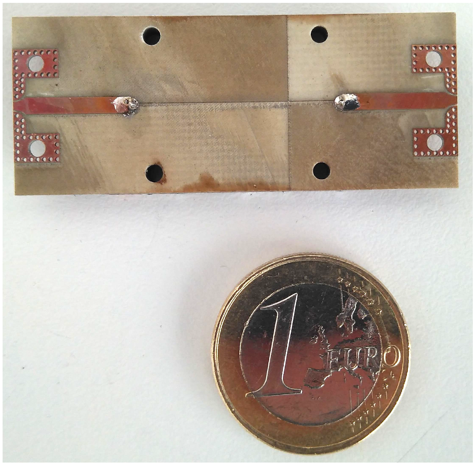
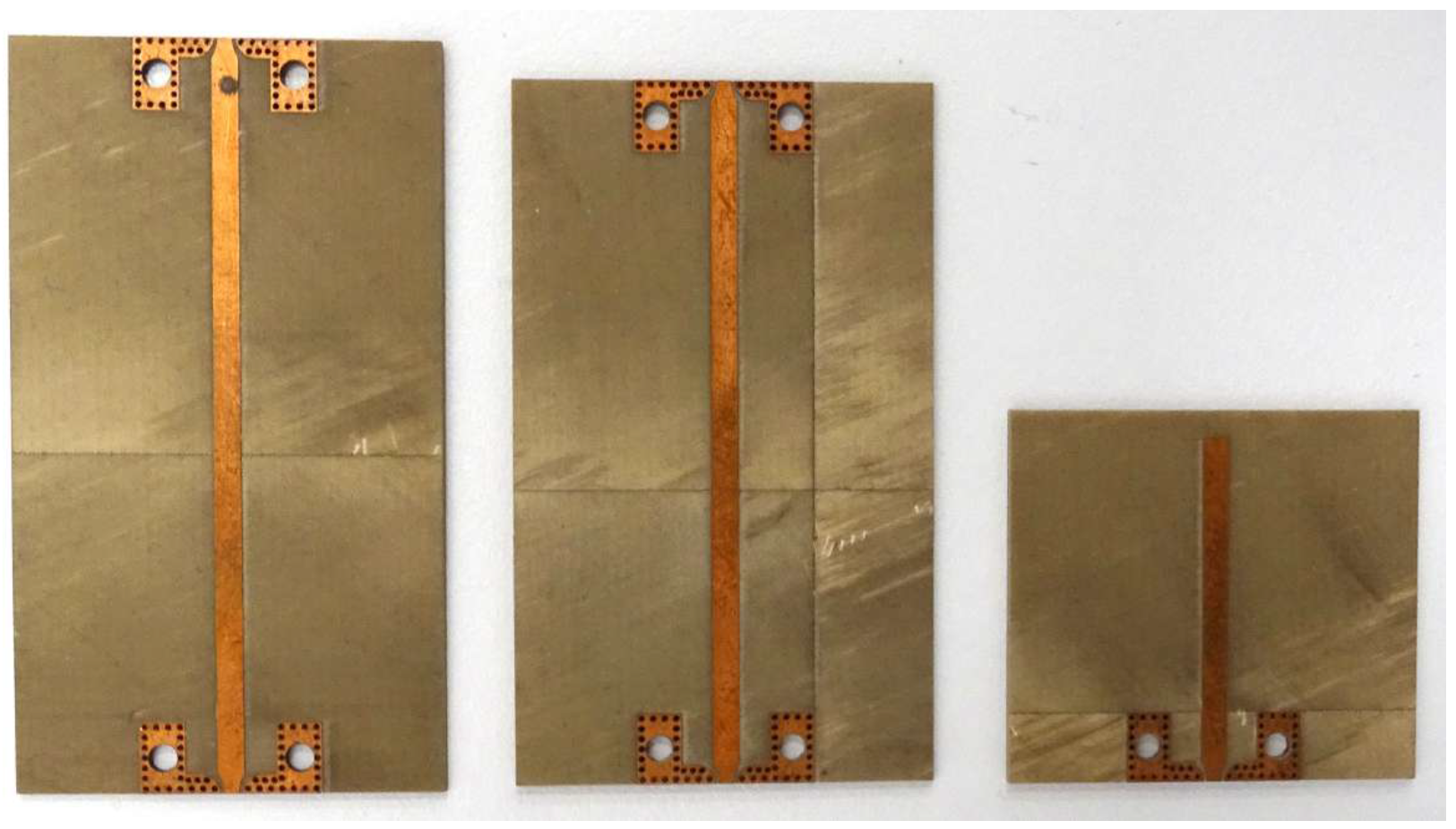
A back-to-back prototype for this second transition has been manufactured to experimentally validate the transition. Layers that compose the prototype can be seen in
Figure 4, whereas the prototype, once built, is shown in
Figure 5 with the reference of a EUR 1 coin to illustrate its real size.
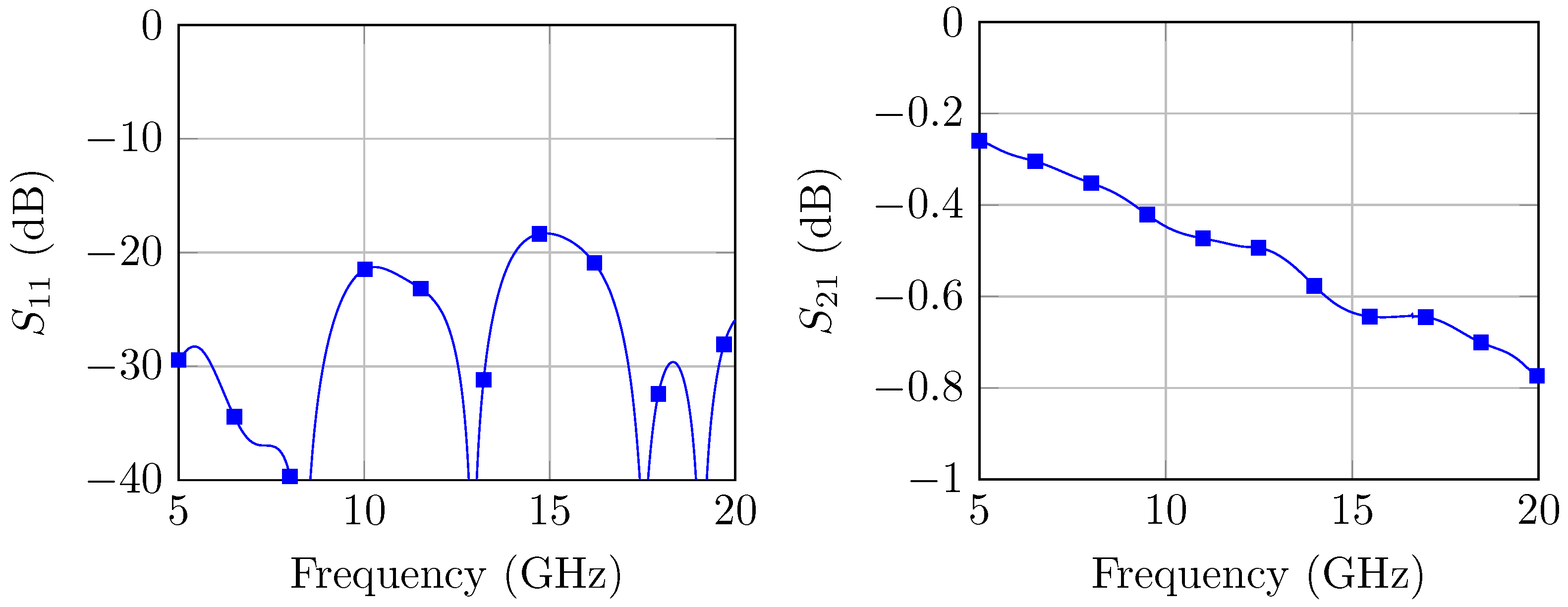
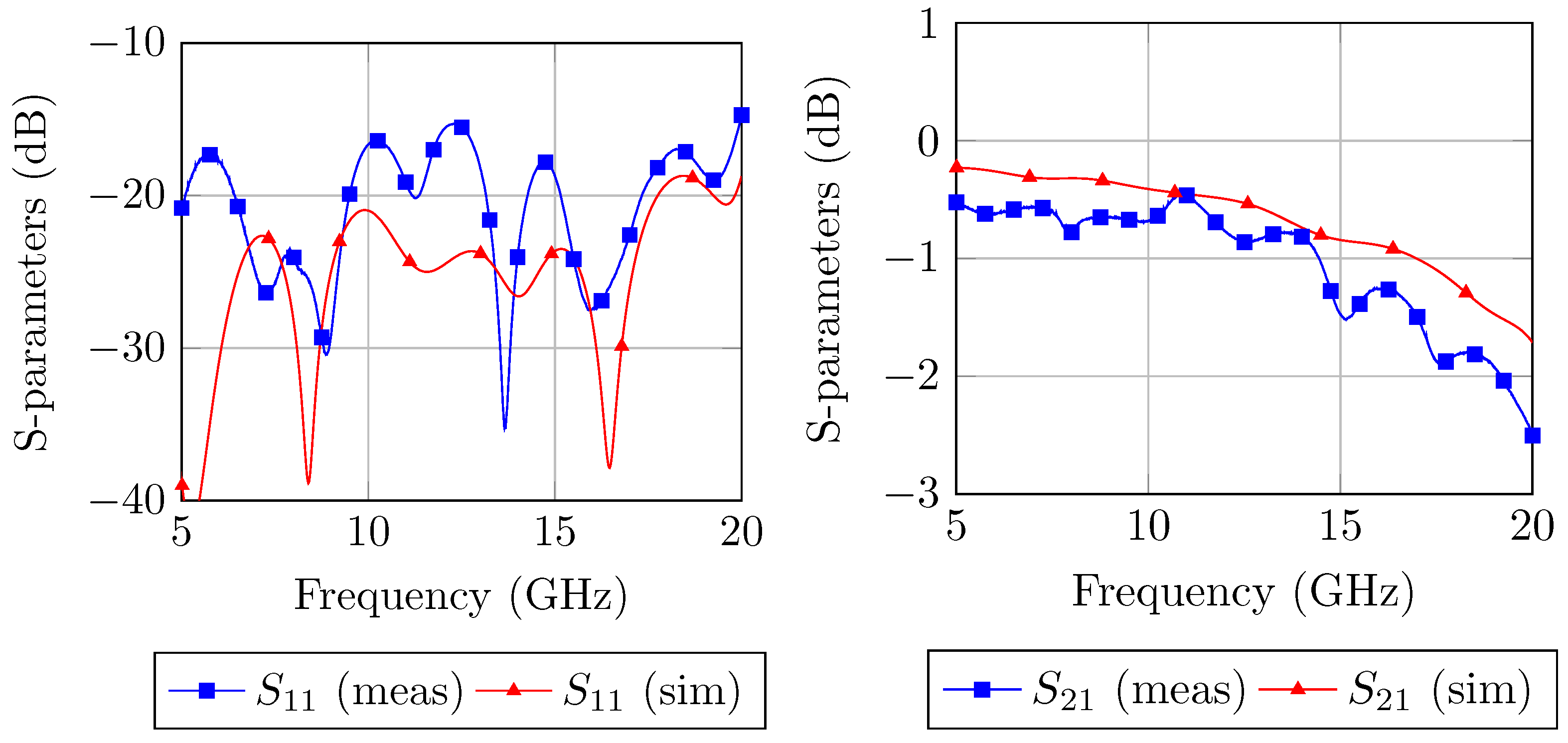
The device was measured with an Anritsu vector network analyzer and a de-embed on the initial microstrip was made using the custom TRL calibration kit shown in
Figure 6. As it is revealed in
Figure 7 there is good agreement between simulation and measurements: return loss is above 15 dB in the whole band of interest (as can be seen in
Figure 7 left), whereas insertion loss is below 1 dB for
14.5 GHz, below 1.5 dB for 14.5
17 GHz and below 2.5 dB for 17
20 GHz (see
Figure 7 right).
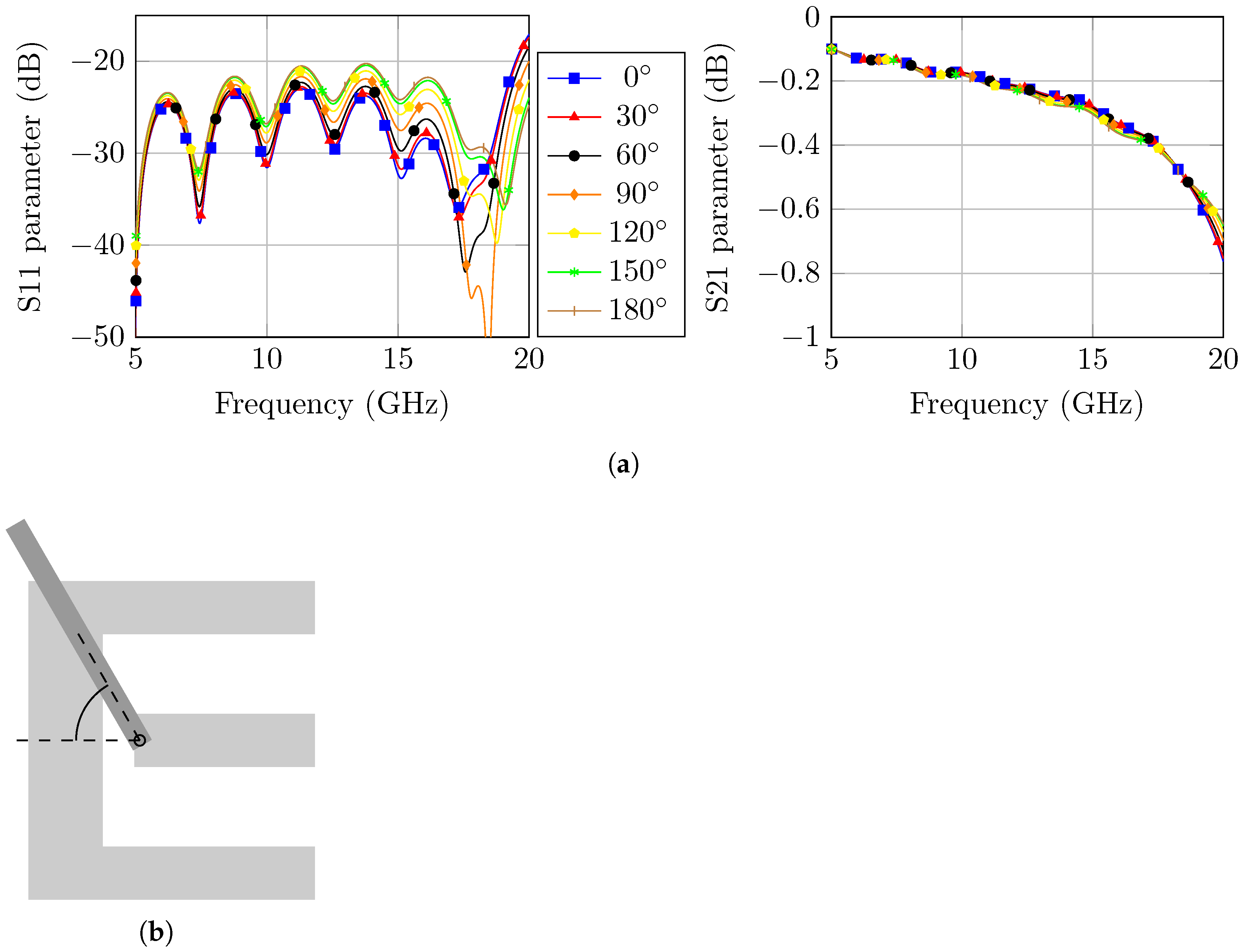
To confirm the independence of the feeding line angle, a parametric simulation was made (considering only one transition, not the whole back-to-back). The angle was swept from
to
in intervals of
. Results shown in
Figure 8 demonstrate the small variation of the reflection coefficient with changes in the angle. As the frequency increases, the evanescent modes that may be excited in the transition have a wider range and are able to store more energy, or in other words, the parasitics related to the feeding angle become more relevant; therefore, slight differences in
can be appreciated around 18 GHz, but they are so small that they are completely negligible and have no effect on the behavior of the prototype. This fact is reinforced in the trend shown for
depending on the angle, which is totally independent of it.
This transition is also extremely robust and tolerant to the variability of the most critical dimensions (those with influence in the gap, the pads and the position of the filament) during the manufacturing process. A yield analysis was carried out considering that those dimensions could present a randomized and independent variation given by manufacturing tolerances; for those variations, it has been assumed a normal distribution with zero mean and standard deviation of 2 (the laser micromachining process tolerance), 25, 50 and 100 microns. Under those constraints, an acceptable performance quality rule has been adopted as having
dB in the passband. The results shown in
Table 3 reveal that this transition is extremely insensitive to small (2 microns) and medium (25 and 50 microns) manufacturing errors and quite acceptable for very high tolerance errors (100 microns).
Table 4 compares this through-wire transition with the other available transitions for ESICL in terms of insertion loss, return loss, electrical length (related to the free-space wavelength at the central frequency
= 10 GHz) and the angle between feeding line and ESICL line. As it can be noticed, this new through-wire transition is equivalent to the others in terms of return loss; it is also equivalent regarding the insertion loss for
14.5 GHz. However, where this through-wire transition is far much better than the others is in its size, as it is electrically much shorter, and in the independence of the incidence angle of the feeding line. Furthermore, the through-wire transition presents also the benefit that the feeding line is placed in the top cover, totally independent of the other layers (even in layer height), and therefore, the whole surface can be used for placing other planar circuits. On the other hand, the manufacturing complexity of this new transition is equivalent to the previous ones, but its design procedure is easier, given that there are no transformers in the feeding line and only four parameters (three of the gap-pad structure and the length of isolation of the inner coaxial) control the final performance of the transition.
4. Conclusions
This paper presents a new through-wire transition from a microstrip feeding line to the ESICL topology. Based on the proposed design procedure, a back-to-back prototype has been manufactured and measured in the band of interest from 0 to 20 GHz; there is a good agreement between simulations and measurements and the results obtained are equivalent to the other previously published transitions to ESICL (GCPW and microstrip), with an insertion loss of less than 2.5 dB and a return loss higher than 15 dB.
The benefits of this easy to design and manufacture novel transition regarding the others are quite advantageous: as the layer of the feeding line is the top cover (totally independent of the layer where the inner coaxial is placed), it can be used to implement other planar circuits; the feeding with the microstrip is possible from any angle, the electrical length of the through-wire transition is 40% smaller than the other transitions and the transition is extremely insensitive to tolerance errors in the manufacturing process.
This transition will surely be an important step towards an easy and efficient integration of traditional planar lines and ESICL, allowing the production of hybrid planar/ESICL integrated circuits, where the advantages of both technologies can be combined.


