Article

In Situ Metrology for Pad Surface Monitoring in CMP Using a Common-Path Phase-Shifting Interferometry: A Feasibility Study

School of Electrical and Electronics Engineering, Chung-Ang University, 84 Heuksuk-ro, Dongjak-gu, Seoul 06974, Korea
*
Author to whom correspondence should be addressed.
Appl. Sci. 2021, 11(15), 6839; https://doi.org/10.3390/app11156839
Submission received: 30 June 2021 / Revised: 18 July 2021 / Accepted: 23 July 2021 / Published: 25 July 2021
(This article belongs to the Special Issue Chemical Mechanical Polishing and Grinding)

Abstract

:

Featured Application

Monitoring of pad surface during CMP process in semiconductor manufacturing.

Abstract

In the fabrication of semiconductors, chemical mechanical polishing (CMP) is an essential wafer-planarization process. For optimal CMP, it is crucial to monitor the texture of the polishing pad; this leads to homogenous planarization of wafers. Hence, we present a new interferometric approach for in situ evaluation of the CMP pad surface based on a common-path phase-shifting interferometry, with which a series of phase-modulated interference signals immune to external perturbation can be recorded. A nanoscopic surface topology can then be reconstructed to estimate surface roughness using the recorded interference images. The surface mapping performance of the proposed method was tested by retrieving a topology of a vibrating nanostructure in immersion, of which height profiles were consistent with the result from atomic force microscopy (AFM). The method was also validated by examining the surface of a used CMP pad in simulated conditions.

Graphical Abstract

1. Introduction

Since Moore’s law [1] stating that the number of transistors per silicon chip doubles every two years, circuits on the chip have increasingly become more integrated and multi-layered, necessitating flatter wafers for the chip substrate, and consequently allowing for higher-resolution photolithography [2]. Chemical mechanical polishing (CMP) is a wafer-planarization technique, in which the wafer is pressurized against a rotating polishing pad in conjunction with chemical slurry; the wafer surface is thus smoothed and flattened through mechanical polishing and chemical reaction [3]. Over the past few decades, CMP has emerged as a critical processing step in advanced semiconductor manufacturing due to a number of advantages in addition to global planarization of the wafer surface [4].
The extent of wafer planarization, however, is affected by the removal rate of wafer material. This removal rate is in turn highly dependent on the roughness of the polishing pad surface, which has numerous micro-asperities [5]. Therefore, it is important to maintain proper surface roughness on the polishing pad during CMP to achieve high quality of wafer flatness. For this purpose, it is imperative to develop metrology that can efficiently assess the roughness of the pad surface in situ. Previously, there have been several measurements of the surface roughness of the CMP pads by obtaining their texture or contour maps using stylus profilometry [6], atomic force microscopy (AFM) [7], scanning electron microscopy (SEM) [6], coherence scanning interferometry (CSI) (often also called white light interferometry (WLI)) [8], and laser scanning confocal microscopy (LSCM) [9]. Despite promising results using these classical metrology technologies [6,7,8,9], the measurements of pad in situ have been scarce; most of the technologies are inaccessible to the pad when CMP is conducted on wet or submerged pads in slurry mixture. A recent effort has shown the possibility of the pad surface measurement under wet conditions using full-field optical coherence tomography (FF-OCT), which is a variant of a high-resolution OCT [10]. Due to the double-arm interferometer utilized in FF-OCT, however, interference is overly sensitive to small external perturbations as a result of separate optical-beam paths. This condition is inappropriate for evaluating the pad in a process exposed to substantial ambient noise such as factory vibration. More recently, advanced confocal technology based three-dimensional (3-D) surface profilers have been developed by several surface metrology companies [11,12,13]. By combining the metrologies with an appropriate immersion objective, the profilers are able to measure the wet pad on the polisher, which is necessary for both lateral beam scanning, using either a rotating multiple pinhole disk [11] or a digital micromirror device (DMD) [12,13]) and vertical scanning of the objective with a piezo drive to generate a 3-D reconstruction of the pad surface.
In this paper, we present a new interferometric method for on-site pad measurement. This novel metrology technique utilizes a common-path phase-shifting interferometry, contributing to existing techniques by enabling precise and reliable evaluation of the pad surface in wet conditions and noisy environments. The surface-mapping performance of the proposed system was tested and validated using a well-known nano-structure. A commercial CMP pad was then examined using the proposed system.

2. Materials and Methods

To enable in situ pad surface monitoring, the proposed method adopted a common-path optical interferometer configuration [14], as shown in Figure 1. Unlike the dual-arm interferometer, the common-path interferometer has a single arm, which is shared by the reference beam and the sample beam. In our set-up, the scheme is achieved by simply placing a light-transparent flat glass over the sample; interference can be generated by a recombination of lights retro-reflected from the glass and the subsequent sample. Importantly, this co-channeling can effectively prevent the interference from fluctuating due to external noise. This is because the lights travelling along the single arm are equally experienced with the perturbation-induced displacement in the optical path length (OPL). Subsequently, due to co-channeling, interference signals are inert to any ambient noise.
As shown in Figure 1, a 700 mW, 637 nm light-emitting diode (LED) (M625L4, Thorlabs Inc. NJ, USA) with a spectral band of 17 nm at full width at half maximum (FWHM; graph inset in Figure 1) was used as a partially coherent light source to generate the interference within a limited coherence gate (or a coherence length). The output beam from the LED was passed through a laser line filter (FL632.8-1, Thorlabs Inc., Newton, NJ, USA) to increase its coherence length. Given that the coherence length lc is defined as ( 2 ln 2 / π ) ( λ 0 2 / Δ λ ) , where λ 0 and Δ λ are a central wavelength and a spectral bandwidth of light, respectively, lc can be increased by reducing its spectral bandwidth. After passing through the filter, the final bandwidth of the beam was reduced to 1.3 nm, theoretically extending lc to approximately 136 μm. The filtered beam was redirected by a beam splitter and then illuminated onto the sample through a 10× water-immersion objective lens (UMPLFLN 10XW, 0.3 N.A., Olympus) and a 1 mm thick microscope slide (a reference glass). The use of a liquid-immersion lens allows the beam to easily penetrate the watery sample in slight contact with the slide, while minimizing strong specular reflections at the glass interfaces and fulfilling the numerical aperture (N.A.). Interference occurs due to the recombination of reflected light waves coming from the bottom of glass and the sample surface, respectively, between which the gap (see Figure 1) filled with a water mixture should be less than the lc overlaid on a confocal gate (a focal plane). Thus, an interference pattern across the illuminated area of sample is projected onto a 2-D pixel array of a CMOS camera (VC-2MC, 2048 × 1088 pixels, Camera Link, Viewworks).
Once the interference pattern was generated, phase-shifting interferometry (PSI)—a well evaluated technique [15]—was applied to the system to obtain the surface structure of the sample. The reference glass—of which one side is firmly attached to a metallic piezoelectric actuator (PZT) with a neodymium magnet—travels axially (up to 150 nm) by sinusoidal oscillation of the PZT at 5 Hz. This results in temporal variation in the magnitudes of the interference signals at each pixel, representing spatial modulation in the interference pattern. Four interference images—resulting from the interference patterns obtained during each quarter of the PZT oscillation period—were captured by the camera at 20 Hz, which had been synchronized with the PZT motion. From the four images E1,2,3,4, phase shifts ϕ , which relied on OPLs between the reference glass and the sample surface, were simply derived as: ϕ ( x , y ) = tan 1 ( E 1 E 2 E 3 + E 4 E 1 E 2 + E 3 + E 4 ) [15], and then phase-unwrapping [16] was followed to resolve 2pi ambiguities in the ϕ . Note that prior to PSI, to compensate for phase error caused by the slope between the reference glass and the sample, the reference glass was pre-aligned to be parallel to the sample stage by identifying a zero-order interference fringe with another microscope slide as a flat sample placed on the sample plate. Given the relative position of the reference glass above the sample, however, the phase shifts may induce a reversed surface shape. To mitigate this inversion issue, an absolute subtraction of the unwrapped phase map was performed with a maximum of the phase shifts. By dividing the corrected phase map by 4 π / λ 0 , eventually, a variation in the physical distances was obtained and re-adjusted based on its mean, which finally was used to describe a surface profile.
However, the configuration of the interferometer used was similar to a Mirau interferometer, which has been used in recent years for the metrology of a patterned wafer [17], thin film [18], and micro electro mechanical systems (MEMS) [19]. Most Mirau interferometers commonly employ a commercial interferometry microscope objective involving a small reference mirror and a beam splitter in the body to generate an equal path length-induced interference for a sample in air. For submerged samples, such as a pad in slurry, however, this arrangement is not suitable for use because when the objective is immersed in the liquid, the sample and reference beam paths may not be identical due to refractive index mismatch between the surrounding media. Thus, interference is not ensured. Furthermore, a highly reflective metallic mirror in the objective may degrade signal contrast in the interference for the inspection of low reflectance materials. In contrast, the proposed interferometer has an individual immersion objective and a movable reference glass, which aides index matching and allows the reference glass to be properly positioned within the coherence length, ensuring high-contrast interference on the submerged materials.

3. Results

3.1. Measurement of System Sensitivity to External Noises

To demonstrate the immunity of the proposed method to external noise, we monitored temporal changes in the interference signal subject to periodic high-frequency (>100 Hz) vibration induced by a mobile phone on the optical table, in addition to intermittent artificial disturbances, caused by low-frequency (few Hz) tapping applied to the corner of the optical table, to mimic industrial noises. We compared the observations with the result from a double-arm Michelson interferometer used in a previous study [9] under the same conditions. The latter was implemented by adding a reference arm to our common-path set-up after removing the reference glass. We measured the intensity of the interference signal as the mean of the pixel values in a 3 × 3 kernel (box) taken at the destructive interference waveform (see inset in Figure 2a). Figure 2a shows time-course interference signal intensities recorded for 8 s using the proposed method and the double-arm interferometer. For a certain interval during vibration (0–3 s), the double-arm system exhibited large fluctuations in magnitude (Video S1). These fluctuations resulted from the concurrent but separate vibration of the different OPLs of the two arms. The fluctuation was greater after 3 s when the optical table was repeatedly tapped by hand along with the vibration. These charts indicate that the traditional interferometric method is prone to interference from external perturbations; therefore, conventional interferometric methods are not suited to evaluate the pad surface in situ. In contrast, the common-path system exhibited relatively minute variations in the magnitude throughout (0–8 s) (Video S2). The small ripples on the waveform may have arisen from intrinsic camera noises such as shot noise. The signal fluctuation was compared with standard deviations (SDs) of the magnitudes for the interval with vibration only (0–3 s), tapping plus vibration (3–8 s), and the whole duration (0–8 s), as shown Figure 2b, in which the SDs of the double-arm system were 9–13 times greater than those of the proposed approach. The results showed that the common-path method was unaffected by any mechanical perturbations, thus resulting in noise-immune interferometry.

3.2. Validation of System Performance

Next, to validate the system’s efficiency in mapping the fine surface profile in wet conditions, we imaged a positive 1951 USAF resolution test target (R3L3S1P, Thorlabs Inc., Newton, NJ, USA). The resolution target was chosen as a well-defined sample with nanoscopic roughness. A water droplet was inserted between the resolution target and the reference glass, and, similar to the processes depicted in Figure 2, the system was exposed to the surrounding vibration during the PSI process. Then, to capture a surface profile for use in reconstruction, the resolution target was also scanned using an atomic force microscope (AFM, XE-100, Park Systems), which is a standard metrology microscope used for high-precision surface mapping. Because the scan range of the AFM is limited to 40 × 40 μm, we selected an area (30 × 30 μm) with a nanoscopic pattern (group 6) printed in chrome on the target substrate prior to AFM imaging; thus, the AFM result was compared with our result from the same region. Figure 3 shows the results of surface imaging. The PSI created four phase-shifted interference images (Figure 3a), from which an unwrapped phase map was derived (Figure 3b). Using Figure 3b, therefore, the surface topology of the target was reconstructed (Figure 3c), and showed height profiles of the patterns on the target. For the pre-selected region, which resembled that depicted in Figure 3d, an enlarged view of the box in Figure 3c was also mapped using AFM, as shown in Figure 3e. Figure 3f presents a graph that displays height profiles taken along the dotted lines in Figure 3e,d, and shows that the height profile derived using the proposed method coincides with that derived using AFM, with the exception of subtle differences on either side of the plateau, for which the averages were 144.79 nm (proposed) and 145.35 nm (AFM). The measurement error to the reference value (145.35 nm) from five repeated measurements averaged 0.37 nm, which represents the measurement accuracy of our system. Moreover, the lateral resolution of the system was measured via a line profile (Figure 3h) taken along a dotted line on the height map (Figure 3g); this resolution was found to be approximately 3 μm from the smallest resolvable pattern (element 6 of group 7). This experiment confirms the capability of the proposed method to accurately capture fine surface profiles even in wet and noisy environments.

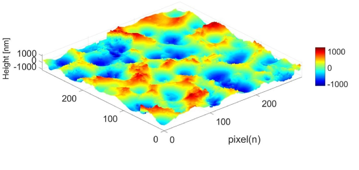
3.3. CMP Pad Surface Measurements Using System

Furthermore, we tested the surface-mapping performance of our system using a perforated anodized aluminum plate with a surface structure similar to that of the pad surface. The surface-mapping results are shown in Figure 4a–d. Figure 4a is a microscope image (300 × 300 μm) of the aluminum plate used in our set-up, showing the microporous surface. Figure 4c is a phase-shift contrast image obtained after a series of post-processing steps using the phase-shifted interference images (Figure 4b), where the darker areas represent deeper valleys in the surface profile. A topology of the mean-referenced surface map is displayed in pseudo color in Figure 4d, delineating the microscopic pores (arrow heads) and asperities (asterisks) on the surface, which correspond to the symbols in positions in Figure 4a.
Finally, CMP-pad imaging was performed using the system. A fully processed (worn out) commercial pad was prepared for imaging; its strip was immersed in diluted water to simulate the use of the polishing pad in a turbid medium, i.e., a slurry mixture. The vibration and tapping on the optical table were repeated to mimic the typical industrial environment. Figure 4e shows a microscope image of the surface of the pad strip in the emulsion. The bright spots (indicated by arrows) in the image result from significant reflectance caused by air bubbles in the pad pores. These air bubbles were removed using a micropipette prior to experiment. Without this step, the highly reflective liquid–air interface may have prevented the generation of interference at the pores, resulting in an error in the measurement of the pad asperity. It has been carefully speculated that the cause of bubble formation in the pores may be air that is accidentally trapped in the immersed pores when the pad with the air-filled pores is immersed in water or subjected to pouring water. This is evidenced by the fact that the gas bubbles in the liquid–solid surface interface tend to stay on the hydrophobic surface, and particularly on the hydrophobic pit sites [20]. Because the pad used in the current study was made of hydrophobic polyurethane, which naturally repels water, the bubbles may preferentially attach to the pores. However, the bubbles may not appear on the pad during CMP because of constant polishing and the influx of chemical slurry particles into the pores. Figure 4f shows a phase-shifted contrast image of the pad surface, from which a pad-surface profile was topographically reconstructed, as shown in Figure 4g. Figure 4g clearly shows the pores and neighboring asperities, which were colder and hotter in color, respectively. These were smoothed and glazed on the surface, implying that the pad surface roughness may be reduced due to the large amount of polishing. For surface analysis, a surface profile of the pad (Figure 4h) was taken along the dotted line in Figure 4g, and its average roughness (Ra) was measured to be 303 nm. This result indicates the applicability of our approach in examining the pad surface during CMP.

4. Discussion

We proposed an interferometric method to investigate the pad surface in CMP, in which a common-path optical interferometer with phase-shifting interferometry was implemented to reconstruct the surface structure of the pad. The proposed system was designed for immersion metrology, which can be easily applied to a submerged sample, and its common-path interferometry is beneficial because the interference is insensitive to external noises. Moreover, the phase-shifting approach does not require mechanical beam scanning, thus allowing the rapid reconstruction of the surface topology. The results showed that our approach was able to provide an areal topology map of a wet or immersed CMP pad, subject to external vibrations that were used to simulate a working environment. This demonstrated an application of the proposed method for in situ inspection of the pad surface roughness during CMP.
A small number of technical issues in the present system remain to be addressed. (1) Although the PZT used was driven by a piezo controller with a positional feedback system, the phase-shifting approach using PZT motion may be unstable, thus preventing the phase gain from being obtained. One method for achieving non-mechanical phase-shifting is to use polarization-base phase shifters consisting of quarter-wave plates and polarizers [21]. Therefore, the common-path interferometer equipped with the polarization optics would allow surface mapping of vibrating pads free of the errors associated with the mechanical motion. (2) The current measurement area, which is limited by the magnification of the objective lens, may not be sufficient to characterize the large surface area of the pad in a working environment. Wide illumination using low N.A. optics may be an appropriate choice for large area measurement, although resulting in a compromise regarding lateral resolution.
Although this preliminary work demonstrated precise and stabilized surface mapping using the proposed technique, significant progress must be made to allow this approach to be applied to commercial CMP tools. Considerable effort will be necessary to integrate the system into the polishers used in production lines, and to improve the system’s capabilities of rapidly acquiring and automatically analyzing data to effectively monitor key pad characteristics. Monitoring these characteristics of the surface roughness, including material removal rate, pad thickness non-uniformities, platen run-out, and groove occlusion, is a long-term but achievable goal.

5. Conclusions

In summary, we presented a new optical metrology technique based on common-path phase-shifting interferometry for in situ measurement of CMP pads. We demonstrated the proposed system’s exceptional capability to restore nano- and microscopic surface structures in wet and/or noisy conditions. We verified the proposed method’s efficiency in mapping surfaces using a commercial polishing pad in a simulated CMP environment. The proposed approach will potentially be adopted and integrated into in situ CMP, for which further research is underway.

Supplementary Materials

The following are available online at https://www.mdpi.com/article/10.3390/app11156839/s1, Video S1: Noise-sensitive interference pattern from the double-arm interferometer, Video S2: Noise-immune interference pattern from the proposed common-path interferometer.

Author Contributions

Conceptualization, W.-J.C. and E.-S.K.; methodology, W.-J.C. and E.-S.K.; software, E.-S.K. and W.-J.C.; validation, E.-S.K. and W.-J.C.; formal analysis, E.-S.K.; investigation, E.-S.K.; resources, E.-S.K.; writing—original draft preparation, E.-S.K.; writing—review and editing, W.-J.C.; supervision, W.-J.C.; project administration, W.-J.C. All authors have read and agreed to the published version of the manuscript.

Funding

This research was funded by the Ministry of Science and ICT, Korea (grant number 2020R1F1A1072912, 2020R1A5A1018052).

Institutional Review Board Statement

Not applicable.

Informed Consent Statement

Not applicable.

Data Availability Statement

Not applicable.

Acknowledgments

We thank Jin-Goo Park for supplying the CMP pad used for this study.

Conflicts of Interest

The authors declare no conflict of interest.

References

  1. Moore, G.E. Cramming more components onto integrated circuits. Electronics 1965, 38, 114–117. [Google Scholar] [CrossRef]
  2. Liau, L.; Muray, A.; Chen, M. Impact of wafer flatness on submicron optical lithography. In Proceedings of the Microlithography Conference, Optical Microlithography VI, Santa Clara, CA, USA, 1 January 1987; Stover, H.L., Ed.; SPIE: Bellingham, WA, USA, 1987. [Google Scholar]
  3. Nanz, G.; Camiletti, L.E. Modeling of chemical-mechanical polishing: A review. IEEE Trans. Semicond. Manuf. 1995, 8, 382–389. [Google Scholar] [CrossRef]
  4. Perry, K.A. Chemical mechanical polishing: The impact of a new technology on an industry. In Proceedings of the 1998 Symposium on VLSI Technology Digest of Technical Papers (Cat. No.98CH36216), Honolulu, HI, USA, 9–11 June 1998. [Google Scholar]
  5. Bastawros, A.; Chandra, A.; Guo, Y.; Yan, B. Pad effects on material-removal rate in chemical-mechanical planarization. J. Electron. Mater. 2002, 31, 1022–1031. [Google Scholar] [CrossRef]
  6. McGrath, J.; Davis, C. Polishing pad surface characterization in chemical mechanical planarization. J. Mater. Process. Technol. 2004, 153–154, 666–673. [Google Scholar] [CrossRef]
  7. Yang, J.C.; Oh, D.W.; Kim, H.J.; Kim, T. Investigation on surface hardening of polyurethane pad during chemical mechanical polishing (CMP). J. Electron. Mater. 2010, 39, 338–346. [Google Scholar] [CrossRef]
  8. Zhao, T.; Yuan, J.; Deng, Q.; Feng, K.; Zhou, Z.; Wang, X. Contrast experiments in dielectrophoresis polishing (DEPP)/chemical mechanical polishing (CMP) of sapphire substrate. Appl. Sci. 2019, 9, 3704. [Google Scholar] [CrossRef] [Green Version]
  9. Zhuang, Y.; Liao, X.; Borucki, L.J.; Theng, S.; Wei, X.; Ashizawa, T.; Philipossian, A. Effect of pad micro-texture on frictional force, removal rate, and wafer topography during copper CMP process. Electrochem. Soc. Trans. 2010, 27, 599–604. [Google Scholar] [CrossRef]
  10. Choi, W.J.; Jung, S.P.; Shin, J.G.; Yang, D.; Lee, B.H. Characterization of wet pad surface in chemical mechanical polishing (CMP) process with full-field optical coherence tomography (FF-OCT). Opt. Express 2011, 19, 13343–13350. [Google Scholar] [CrossRef] [PubMed]
  11. Hamann, G. Optical 3D Surface Measuring Technology: Accurate Profile Reproduction of the Finest Structures Thanks to Piezo Technology and Confocal Technology. Available online: http://onlinelibrary.wiley.com/doi/pdf/10.1002/opph.201500007 (accessed on 14 July 2021).
  12. Matilla, A.; Mariné, J.; Pérez, J.; Cadevall, C.; Artigas, R. Three-dimensional measurements with a novel technique combination of confocal and focus variation with a simultaneous scan publication. In Proceedings of the SPIE Photonics Europe, Optical Micro- and Nanometrology VI, Brussels, Belgium, 3–7 April 2016; Gorecki, C., Ed.; SPIE: Bellingham, WA, USA, 2016. [Google Scholar]
  13. Application Note: In-situ Metrology for Pad Surface Monitoring in CMP. Available online: https://www.sensofar.com/wp-content/uploads/2015/07/App-note-S-mart-CMP.pdf (accessed on 14 July 2021).
  14. Park, J.S.; Chen, Z.; Jung, M.Y.; Kim, C.S. Double common-path interferometer for flexible optical probe of optical coherence tomography. Opt. Express 2012, 20, 1102–1112. [Google Scholar] [CrossRef] [PubMed]
  15. Dubois, A. Phase-map measurements by interferometry with sinusoidal phase modulation and four integrating buckets. J. Opt. Soc. Am. A 2001, 18, 1972–1979. [Google Scholar] [CrossRef] [PubMed]
  16. Costantini, M. A novel phase unwrapping method based on network programming. IEEE Trans. Geosci. Remote Sens. 1998, 36, 813–821. [Google Scholar] [CrossRef]
  17. de Lega, X.C.; de Groot, P. Optical topography measurement of patterned wafers. In Proceedings of the Characterization and Metrology for ULSI Technology 2005, Richardson, TX, USA, 15–18 March 2005; Seiler, D.G., Ed.; AIP: College Park, MD, USA, 2005. [Google Scholar]
  18. Fay, M.F.; Dresel, T. Applications of model-based transparent surface films analysis using coherence-scanning interferometry. Opt. Eng. 2017, 56, 111709. [Google Scholar] [CrossRef] [Green Version]
  19. Albero, J.; Bargiel, S.; Passilly, N.; Dannberg, P.; Stumpf, M.; Zeitner, U.D.; Rousselot, C.; Gastinger, K.; Gorecki, C. Micromachined array-type Mirau interferometer for parallel inspection of MEMS. J. Micromech. Microeng. 2011, 21, 065005. [Google Scholar] [CrossRef]
  20. Meng, D.D.; Kim, J.; Kim, C.-J. A degassing plate with hydrophobic bubble capture and distributed venting for microfluidic devices. J. Micromech. Microeng. 2006, 16, 419–424. [Google Scholar] [CrossRef] [Green Version]
  21. Ngoi, B.K.A.; Venkatakrishnan, K.; Sivakumar, N.R. Phase-shifting interferometry immune to vibration. Appl. Opt. 2001, 40, 3211–3214. [Google Scholar] [CrossRef] [PubMed]
Figure 1. A schematic of the implemented system for CMP pad surface measurement. PZT, piezo electric actuator. lc, coherence length. Insets (left top and right) are a spectrum of the light source and a picture of the common-path of the system, respectively.
Applsci 11 06839 g001
Figure 2. Interference signal stabilization using the proposed method. (a) Time-course interference signal intensities in the presence of surrounding noise (0–3 s vibration, 3–8 s vibration + tapping). Despite the external noise, the signal magnitude (red line) is stabilized by the proposed common-path interferometer (Video S2), whereas for the existing double-arm interferometer, the magnitude (dotted line) experiences considerable fluctuations (Video S1). (b) Comparison of the fluctuation in magnitudes with the corresponding standard deviations for each interval.
Applsci 11 06839 g002
Figure 3. Surface-mapping performance of the proposed method. (a) Phase-shifted interference images of a positive 1951 resolution test target immersed in water and exposed to external noise during PSI. (b) An unwrapped phase map of the test target, including the physical height of the nanoscopic pattern on the target. (c) The height map reconstructed from (b). (d) A magnification of the height map of the boxed area in (c), and the same region scanned with AFM (e). (f) Height profiles taken along the dotted line in (e,d), respectively. (g) A 3-D view of (c). (h) A 1-D height profile taken along the dotted line in (g).
Applsci 11 06839 g003
Figure 4. Surface mapping of a pad-like sample and a used CMP pad. (a) A microscope image (300 × 300 μm) of the porous surface of an anodized aluminum plate. (b) Phase-shifted interference images of the plate. (c) A phase-shifted contrast image. (d) A topology of the surface map. (e) A microscope image of the processed CMP pad surface immersed in a diluted emulsion, where arrows indicate the top of air bubbles trapped in the pores, which were removed before PSI. (f) A phase-shifted contrast image of the CMP pad surface. (g) The topology of the CMP pad surface map. (h) A 1-D surface profile taken along the dotted line in (g).
Applsci 11 06839 g004
Publisher’s Note: MDPI stays neutral with regard to jurisdictional claims in published maps and institutional affiliations.

