Article

Enhanced Coupling Coefficient in Dual-Mode ZnO/SiC Surface Acoustic Wave Devices with Partially Etched Piezoelectric Layer

Key Laboratory of Advanced Materials (MOE), School of Materials Science and Engineering, Tsinghua University, Beijing 100084, China
*
Authors to whom correspondence should be addressed.
Appl. Sci. 2021, 11(14), 6383; https://doi.org/10.3390/app11146383
Submission received: 24 May 2021 / Revised: 30 June 2021 / Accepted: 8 July 2021 / Published: 10 July 2021
(This article belongs to the Special Issue Element-Based Methods for the Solution of Engineering Problems)

Abstract

:
Surface acoustic wave (SAW) devices based on multi-layer structures have been widely used in filters and sensors. The electromechanical coupling factor (K2), which reflects energy-conversion efficiency, directly determines the bandwidth of the filter and the sensitivity of sensor. In this work, a new configuration of dual-mode (quasi-Rayleigh and quasi-Sezawa) SAW devices on a ZnO/SiC layered structure exhibiting significantly enhanced K2 was studied using the finite element method (FEM), which features in the partial etching of the piezoelectric film between the adjacent interdigitated electrodes (IDTs). The influences of piezoelectric film thickness, etching ratio, top electrodes, bottom electrodes, and the metallization ratio on the K2 were systematically investigated. The optimum K2 for the quasi-Rayleigh mode and quasi-Sezawa mode can exceed 12% and 8%, respectively, which increases by nearly 12 times and 2 times that of the conventional ZnO/SiC structure. Such significantly promoted K2 is of great benefit for better comprehensive performance of SAW devices. More specifically, a quasi-Rayleigh mode with relatively low acoustic velocity (Vp) can be applied into the miniaturization of SAW devices, while a quasi-Sezawa mode exhibiting a Vp value higher than 5000 m/s is suitable for fabricating SAW devices requiring high frequency and large bandwidth. This novel structure has proposed a viable route for fabricating SAW devices with excellent overall performance.

Graphical Abstract

1. Introduction

With the rapid development of smart terminals and human information society [1,2,3,4,5], surface acoustic wave (SAW) devices are comprehensively applied in Radio Frequency (RF) filters, sensors, and microfluidics due to their miniature size, low cost, and steady performance [6,7,8]. For the sake of SAW devices with more practical value, researchers continue to explore innovative structures and materials. Furthermore, compared to SAW devices mainly made of bulk piezoelectric substrates, multi-layer substrate has attracted extensive attention due to its high acoustic velocity and suitable piezoelectricity, which combines the merits of the piezoelectric layer, high velocity substrate, and other functional layers [9,10,11].
In SAW devices, ZnO and AlN are widely used as piezoelectric film materials, while non-piezoelectric substrates with high acoustic velocity include Si, sapphire (Al2O3), SiC, diamond, and so on [12]. Among these combinations of piezoelectric films and substrates, ZnO/SiC structure devices have attracted the attention of researchers because ZnO possesses good piezoelectricity and moderate velocity while SiC exhibits a high velocity (~12,500 m/s), low propagation loss, and high thermal conductivity (~490 W·m−1·K−1), which is necessary for the fabrication of high performance devices. Moreover, the lattice mismatch between SiC (a = 3.073 Å, c = 15.120 Å) [13] and ZnO (a = 3.249 Å, c = 5.206 Å) [14] piezoelectric films is as small as 5%, which simplifies device preparation [15]. Our previous work reported a SAW filter that shows high SAW velocity with a working frequency as high as 6.8 GHz [16]. Nevertheless, acoustic waves propagating from a conventional ZnO/SiC layered structure suffer from low K2. As the calculated results show, the K2 value of the Rayleigh mode is less than 0.8%, and that of the Sezawa mode is no more than 3.2%.
The explosive growth of data transmission volume proposes a higher filter requirement, especially wideband filters. For SAW sensor applications, more sensitive sensors have traditionally been targeted. Since K2 is a decisive factor in the filter bandwidth and sensor sensitivity, pursuing a higher K2 is necessary for the needs of wideband filters and high sensitivity sensors. In order to meet the increasing demands of wideband filters in mobile communication, pursuing a higher K2 is necessary. In recent years, many studies have been committed to improving the K2 in multi-layer substrate SAW devices. First, enhancing the piezoelectric response of the piezoelectric film can cause an increase in the K2 of the SAW resonators. Doping is a widely used approach for improving piezoelectric response. Many kinds of elements such as Sc [17], Ti [18], Y [19], and Ta [20] have been studied as dopants for AlN. It is reported that doping Fe [21], Cr, and V [22] can also improve the piezoelectric coefficient of ZnO. However, doping sometimes leads to a low quality factor and decreased acoustic velocity [23]. In addition, developing a new configuration of multi-layer substrate is another promising way to obtain higher K2 [23]. Over the past few years, many imaginative structures have been proven to achieve good performance, including embedding the top electrodes under SiO2 [10,24], burying the top electrodes into the grooves on the piezoelectric film [25], optimizing the transducer topology [26], and so on. Recently, a new configuration of hybrid SAW/bulk acoustic wave (BAW) structure has been reported that also shows an enhanced K2 [27]. Since ZnO/SiC structure is a potential structure for building high performance devices, promoting a simpler and more effective way to enhance the K2 of this structure is necessary.
In this work, we simulated a novel structure with partially etched piezoelectric thin film between adjacent top interdigitated electrodes in the interdigitated electrodes (IDTs)/ZnO/SiC multi-layer configuration in order to increase the K2 of the SAW devices. Dual modes of the etching structure were both investigated systematically. The displacements of the two modes along the y direction (uy) were close to zero, while their longitudinal (uz) and vertical shear components (ux) were dominant. The displacement characteristics of the first mode and second mode are similar to those of the Rayleigh mode and Sezawa mode, respectively, checked and analyzed by the displacement field distribution [28,29]. Thus, the two modes are called quasi-Rayleigh and quasi-Sezawa mode, respectively, due to their propagation features [10,16], and both of them possess significantly enhanced K2 compared to the classical modes of the unetched structure. Our results propose a promising way to achieve the miniaturization of SAW devices in low frequency bands using the quasi-Rayleigh mode, and in high frequency and wideband SAW devices using quasi-Sezawa mode as well as high sensitivity sensors utilizing high K2.

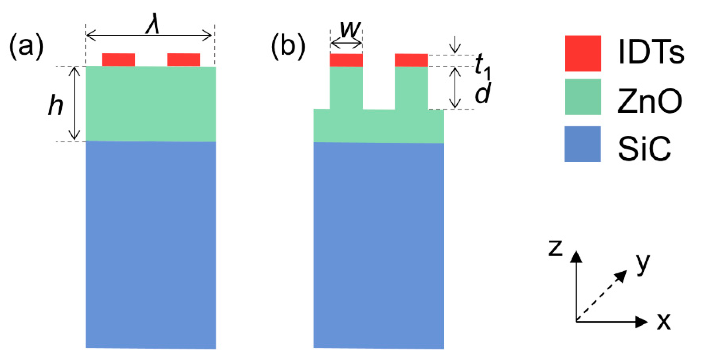
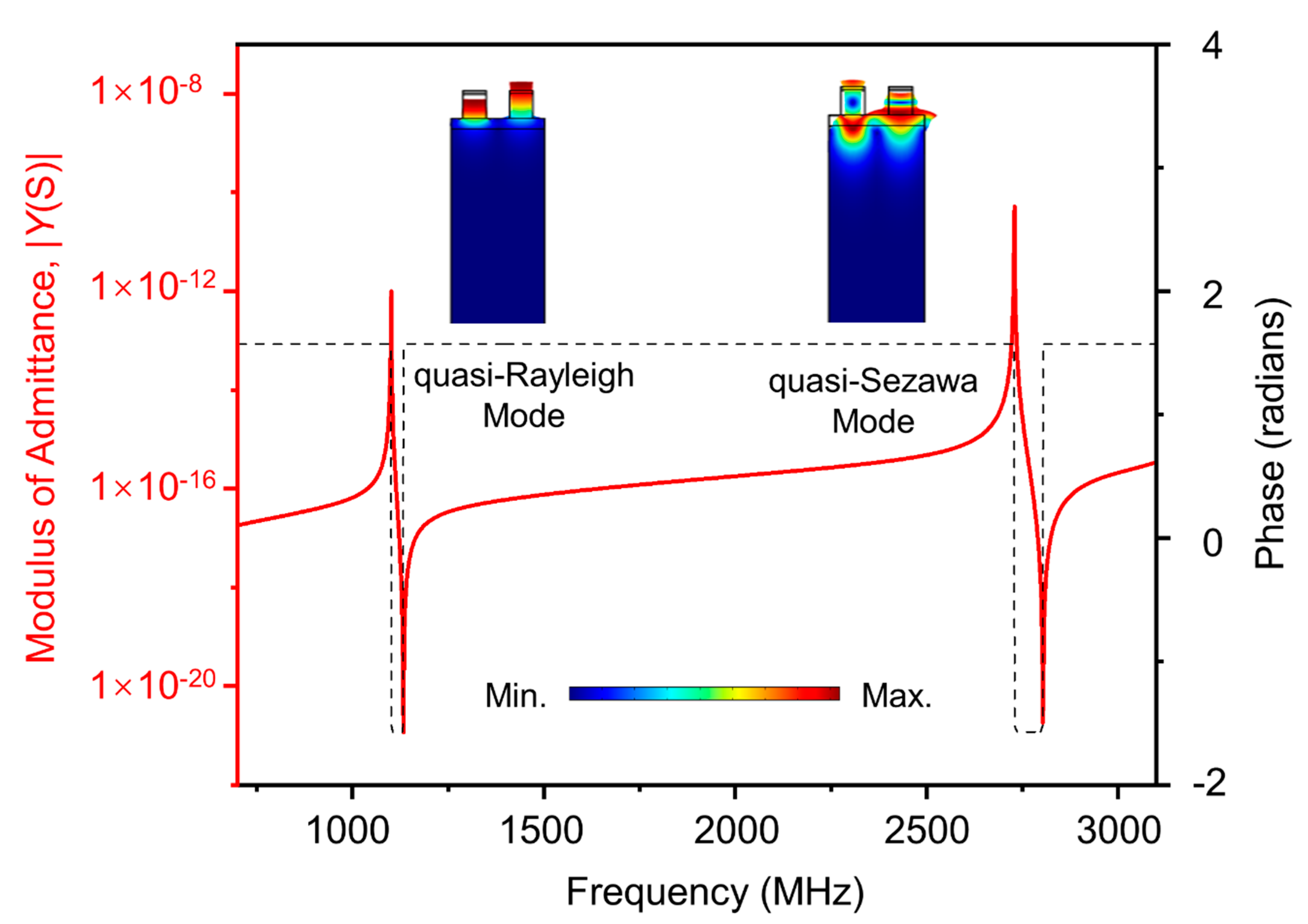
2. Materials and Methods
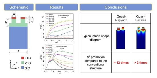
The schematic of conventional IDTs/ZnO/SiC configuration and our proposed structure are depicted in Figure 1a,b. Compared to the traditional multi-layer structure in SAW devices, piezoelectric thin film between the adjacent top interdigitated electrodes is partially removed in this work, as depicted in Figure 1b. The commercial finite element method (FEM) software COMSOL Multiphysics was used to obtain the SAW characteristics of the proposed structure. A three-dimensional model that uses a periodic component of the practical resonator’s structure was established The width of the model was one wavelength, and the wavelength λ was fixed at 2 μm. The thicknesses of the total ZnO piezoelectric film and the etching depth were h and d, respectively. The etching ratio d/h was used to express the proportion of the etched part to the whole piezoelectric film. The electrode’s width was represented by w, and the retained ZnO pillars’ width was consistent with the electrode. The model’s size at the y-axis was set as 0.25λ. The periodic boundary condition was applied in both the x- and y- direction to assume infinite length. The PML was fixed at the bottom of SiC substrate to eliminate the reflection of acoustic waves at the bottom boundary. The material constants of ZnO and SiC were obtained from Ref. [16]. The influences of Al, Cu, Pt, Mo, W, and Au as electrode materials were also investigated, and their properties were from COMSOL database.
All parts except the two electrodes were included in the electrostatics. One electrode was set as the terminal electrical condition with voltage +1 V, and the other one was ground. The |Y(S)| spectra were derived through the frequency domain calculation.
The effective phase velocity (Vp) of the resonator is estimated through the formula [24]:
V p = λ f r + f a 2
The effective electromechanical coupling coefficient K2 is calculated by [11,30]:
K 2 = π f r 2 f a / tan ( π f r 2 f a )
where fr and fa are the resonant frequency and anti-resonant frequency corresponding to the local maximum and local minimum in the |Y(S)| spectra, respectively.
Figure 2 shows a typical input admittance curve and phase curve of the partially etched ZnO/SiC configuration when the ZnO piezoelectric film normalized thickness h is 0.6λ and the etching ratio d/h is 0.7. There are two resonant modes in the admittance spectrum, and the center frequency of each mode is 1.12 GHz and 2.77 GHz. The insets depict the simulated mode shape diagrams of the above two modes at their resonant frequencies. It was found that both of their propagation characteristics are similar to those of the Rayleigh and Sezawa modes of the conventional structure. As observed from the deformation shape, different from conventional SAW structure, the SAW propagation is not obvious in this structure. This is because when the piezoelectric films are etched to the pillars, each pillar works as a BAW resonator. The vibration of the BAW in the z direction dominates the resonance, and only a small part of acoustic energy is transformed into a SAW. Similar results have been reported by Zhang et al. [31] and Pashchenko et al. [27]. In order to distinguish the conventional structure modes , it is better to call the first order mode quasi-Rayleigh and the second order mode quasi-Sezawa mode [31].

3. Results

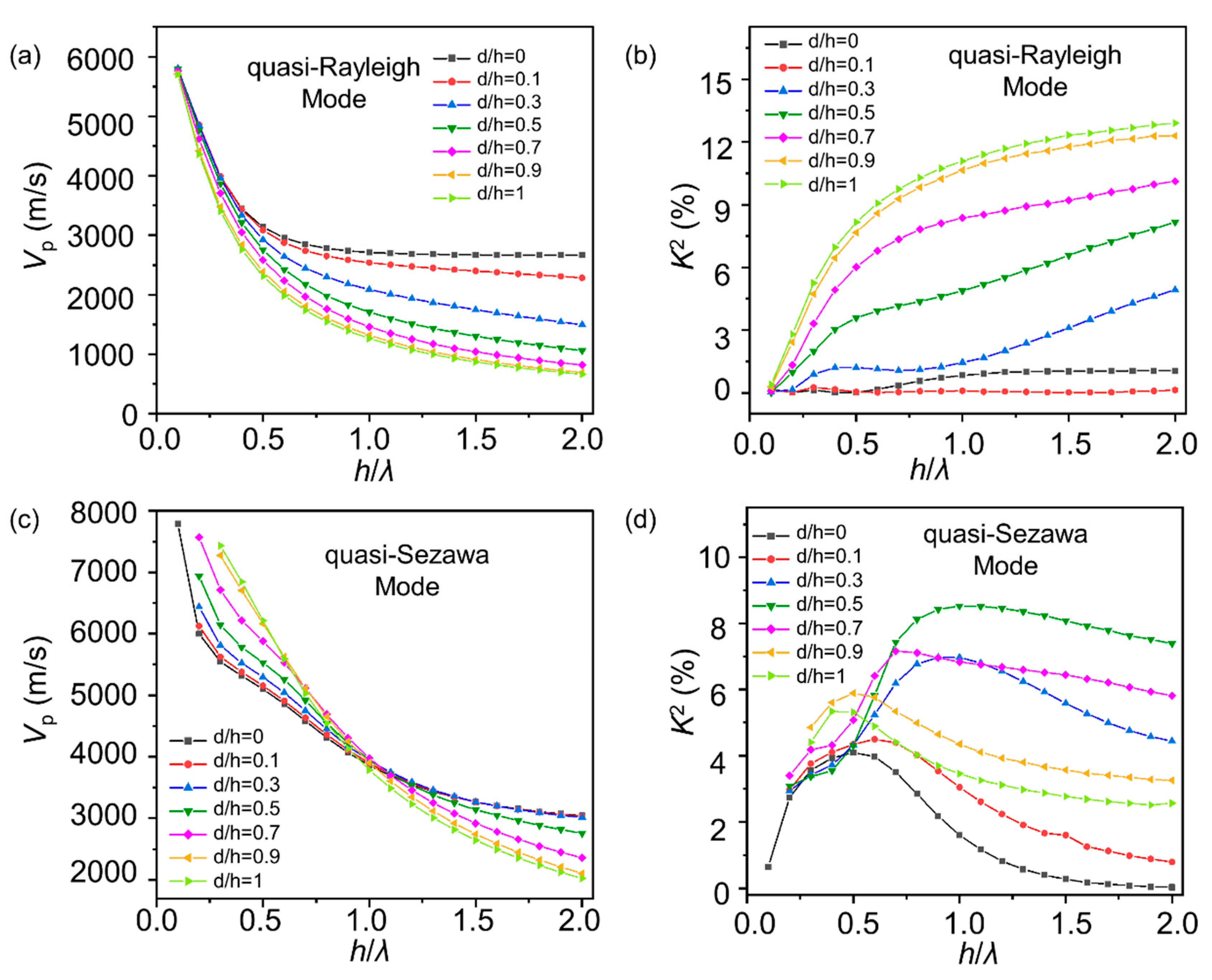
3.1. Etching Ratio and Piezoelectric Film Thickness
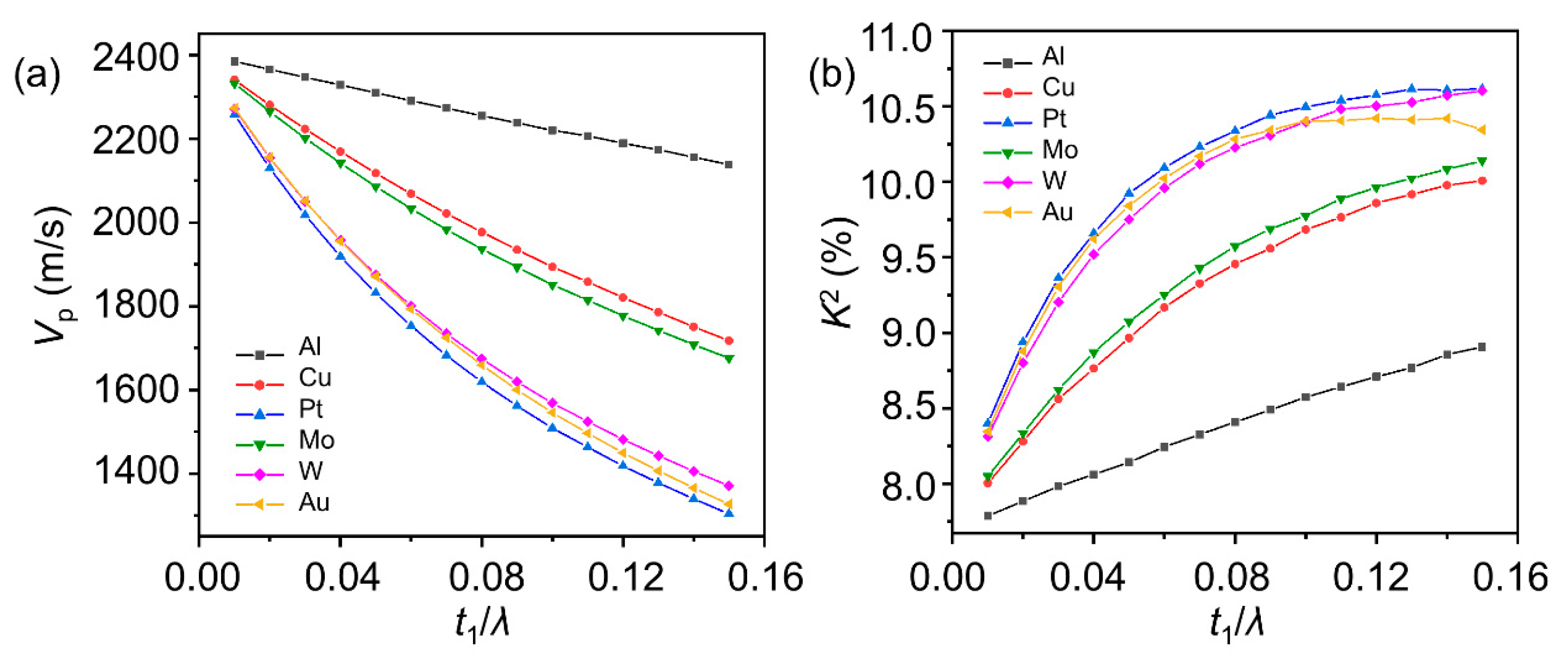
We first analyzed the propagation characteristics when the etching ratio and ZnO film thickness change. The variation of Vp and K2 in both modes as functions of ZnO thickness in different etching ratio conditions when the top Al electrode thickness t1 = 0.05λ was studied and shown in Figure 3. All of the results presented in Figure 3, Figure 4 and Figure 5 were simulated when the metallization ratio 2w/λ was equal to 0.5. The d/h = 0 represents the condition of the conventional structure. It can be seen in Figure 3a that regardless of the etching ratio d/h, the Vp value of the quasi-Rayleigh mode decreases monotonically as the ZnO thickness h increases. This is due to the fact that SiC exhibits a much larger velocity compared tothat of ZnO. When the ZnO film is totally etched into pillars on the substrate, the Vp value declined to a minimum value compared to other etching ratios at the same ZnO normalized thickness. As for the K2, as Figure 3b shows, when the etching ratio is beyond 50%, the K2 value sees an obvious increment and peaks at d/h = 1. When the etching ratio is below 50%, the K2 value improved weakly or was even worse than that of the conventional structure. Since the higher etching ratio and larger ZnO thickness both contribute to the growth of K2, the maximum K2 value is 12.90%, as the d/h = 1 and h/λ = 2 in Figure 3b. However, during these conditions, the Vp is extremely low, only 662.2 m/s. As Figure 3c,d shows, with the increase of ZnO thickness, the velocity continues to decrease, while the K2 of the quasi-Sezawa mode reaches the maximum value in the beginning and then decreases for each branch. The maximum K2 value of the quasi-Sezawa mode is 8.52%, appearing at d/h = 0.5 and h/λ = 1.
It can be seen from Figure 3 that the combinations of different etching ratios and ZnO thicknesses bring a rich diversity of Vp and K2, providing a variety of design possibilities. However, considering that the overall small aspect ratio w/d in the actual preparation causes the etching process to be complicated and may even cause the structure to collapse, the trade-off between the desired performance and fabrication difficulty must be taken into consideration. Moderate parameters d/h = 1 and h/λ = 0.5 were chosen for the further optimization of quasi-Rayleigh mode in which a high K2 value of 8.16% and Vp of 2309.8 m/s were obtained. Meanwhile, d/h = 0.7 and h/λ = 0.6 were chosen for the further optimization of quasi-Sezawa mode, in which the values of Vp and K2 reach about 5532.0 m/s and 6.40% respectively.

3.2. Top Electrodes

Next, we investigated how the material type and thickness of the top electrodes influenced the properties of the quasi-Rayleigh mode. As Figure 4 shows, with the growth of top electrode thickness, the Vp value decreases while the K2 value increases monotonically for most electrode materials. The K2 curve of Au as a function of top electrode thickness first exhibits an increasing trend and then a decreasing trend. When the height of the electrode is fixed, K2 increases with increasing electrode thickness, which is accompanied by the reduction of Vp. As shown in Figure 4, top Pt electrodes exhibit the strongest loading effect. They lower the Vp the most sharply and enhance the K2 the most significantly as their thicknesses increase. When the thickness of the Pt electrode t1 reaches 0.12λ, its K2 is rather constant at around 10.60% with increasing electrode thickness. As for Pt, Au and W and Cu and Mo, their Vp and K2 curves are also very close. This is owing to the fact that the mass loading effect of different electrode materials is in full proportion to their densities [32]. Cu possesses superior electrical conductivity and low cost, while maintaining a high K2 simultaneously. The utilization of Cu electrodes is often reported in wideband SAW filters [8,30] and TCSAWs [33,34]. Thus, it was chosen for the subsequent optimization of quasi-Rayleigh. Since the top Cu electrode thickness t1/λ is 0.07, the Vp is 2021.1 m/s and the K2 is 9.32%.
Figure 5 shows the change of the Vp and K2 of the quasi-Sezawa mode with the normalized top electrode thickness when the etching ratio is d/h = 0.7 and the ZnO thickness is h/λ = 0.6. For most electrode materials, similar with Figure 4a, the Vp decreases monotonically with the increase of electrode thickness. As for the K2, an increasing trend can be seen at first, followed by a decreasing trend, as shown in Figure 5b. Nevertheless, the Vp and K2 dispersion curves of Au both exhibit an abnormal fluctuation as the functions of the top electrode thickness. Meanwhile, when Au is utilized as the top electrode material, its Vp and K2 change more dramatically with the top electrode thickness compared to other electrode materials. The maximum K2 appears at different electrode thicknesses for individual electrodes, but each K2max value is about 6.80% similar. Among them, when the top electrode material is Al, the Vp decreases slowly as its thickness increases. Simultaneously, K2 varies in a small range but keeps a relatively high value with changes in thickness to the top Al electrode. As the top Al electrode thickness t1/λ is 0.11, the Vp is 5407.3 m/s and the K2 is 6.78%, which is quite an exciting value compared to the conventional ZnO/SiC structure using Al electrodes. In the previous structure, the K2 of the Sezawa wave is only ~3.6% when the Vp is of the same value as the optimized configuration, indicating that partially etching the structure is an effective way to enhance the K2 of the ZnO/SiC substrate and a promising solution for the fabrication of SAW devices using high frequencies and wide bands.

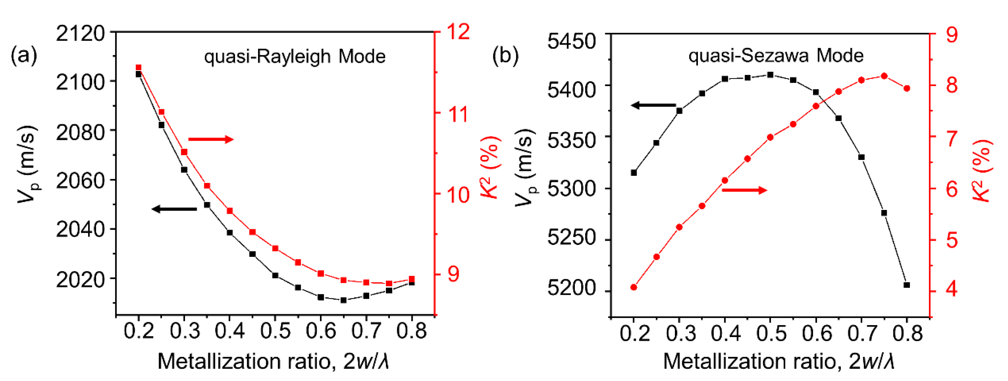
3.3. Metallization Ratio

The influence of the metallization ratio on the resonator is also studied. Compared to the above-mentioned factors such as ZnO normalized thickness and top electrode material and thickness, the metallization ratio 2w/λ has a relatively small effect on the velocity, but it significantly impacts the K2 of both modes. For better optimization, quasi-Rayleigh mode and quasi-Sezawa mode were simulated under different conditions. Quasi-Rayleigh mode was simulated when changing the metallization ratio to ZnO normalized thickness h/λ = 0.5, etching ratio d/h = 1, and top Cu electrode normalized thickness t1/λ = 0.07. As shown in Figure 6a, Vp and K2 of quasi-Rayleigh both exhibit a relatively sharp declining trend at first and then increase slightly. As such, a smaller top electrode width as well as the ZnO pillar width is beneficial to improving the K2 of the quasi-Rayleigh. When the metallization ratio was 0.2, K2 reached 11.56% which accompanied a Vp value of 2102.8 m/s. Quasi-Sezawa mode was simulated when changing metallization ratio to ZnO normalized thickness h/λ = 0.6, etching ratio d/h = 0.7, and top Al electrode normalized thickness t1/λ = 0.11. Figure 6b depicts that the Vp and K2 of the quasi-Sezawa mode initially increase and then decline monotonically with an increasing metallization ratio in contrast to the quasi-Rayleigh. K2 achieved a maximum value of 8.17% when the metallization ratio was 0.75, simultaneously, the Vp value was 5276.0 m/s.

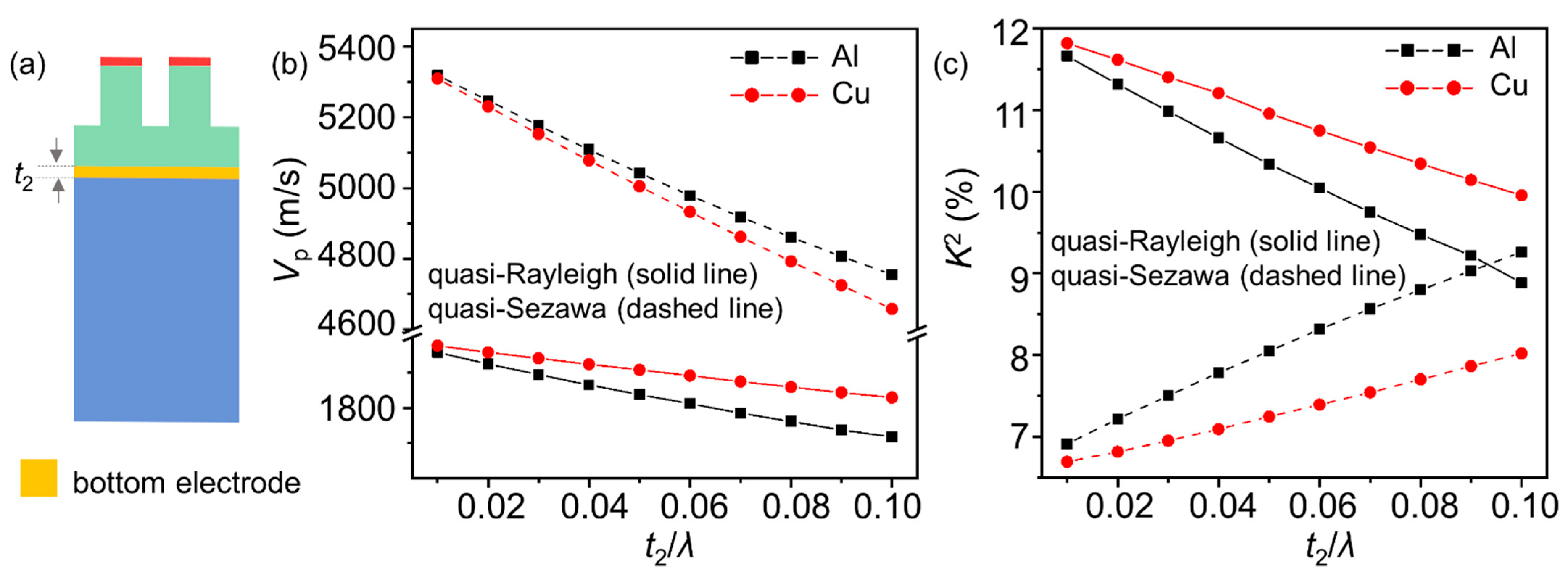
3.4. Bottom Electrodes

In a traditional multi-layer structure, an additional bottom electrode with floating potential often helps improve the K2 of the resonator [35,36,37]. For the proposed structure in this study, introducing a bottom electrode with floating potential formed a structure called hybrid quasi-SAW/BAW configuration [31], illustrated by Figure 7a. For simplicity, the two modes in the new structure with the bottom electrode are named as quasi-Rayleigh and quasi-Sezawa mode. For further study on the impacts of the thickness and material of the bottom electrode, different conditions were considered for each mode, and these specific situations were consistent with those of the previous section, as the metallization ratio of the two modes was still 0.5. Figure 7b shows that the Vp value goes down with the growth of the bottom electrode thickness for both modes. This is due to the fact that the acoustic velocity of the bottom metal electrode is much lower than SiC, and the high acoustic velocity of the substrate cannot be better taken advantage of when surface acoustic waves propagate. The acoustic velocity of the hybrid quasi-SAW/BAW structure must be lower than that of the same structure without a bottom electrode. Figure 7c depicts the K2 of the quasi-Rayleigh mode, which decreases monotonically with growing bottom electrode thickness, while the K2 of the quasi-Sezawa mode exhibits the contrary trend. Compared to the same etched structure without a bottom electrode, K2 of the hybrid quasi-SAW/BAW configuration does not always increase. For the quasi-Rayleigh mode, bottom Cu electrode exhibits a better behavior than Al, and the maximum K2 value of 11.82% can be achieved when the thickness is negligible. At the same time, the Vp of the quasi-Rayleigh mode is 1975.8 m/s, which indicates adding a bottom electrode is a feasible choice to further increase the K2 of the quasi-Rayleigh mode. For the quasi-Sezawa mode, a bottom Al electrode can achieve higher K2 than Cu, and the K2 value can be boosted to 9.26% when the normalized thickness of the bottom Al electrode is 0.1, however, at the same time, the value of Vp decreases to 4754.8 m/s. Compared to the structure without a bottom electrode, the trade-off between the Vp and K2 of the quasi-Sezawa mode should be taken into consideration. A specific choice of bottom electrode material and thickness can significantly improve the K2 by 36.6%, though at the cost of sacrificing Vp of 12.1% compared to the case when the top Al electrode thickness t1/λ = 0.11, the etching ratio d/h = 0.7 and ZnO thickness h/λ = 0.6 based on the partially etched ZnO/SiC structure without a bottom electrode.

4. Discussion

This work proposed a new configuration for SAW devices based on the partially etched ZnO/SiC structure. Diverse combinations of piezoelectric layer thickness, etching depth, electrode material, and metallization ratio provide many choices for practical use. We demonstrated the optimization of the proposed structure. As the quasi-Rayleigh mode wave and the quasi-Sezawa mode wave are distanced in the frequency domain and do not interfere with each other, they can be used individually and can exert their respective functions. Primarily, choosing a proper piezoelectric film thickness and etching ratio is the most necessary consideration. For the quasi-Rayleigh mode, higher ZnO thickness and etching depth both contribute to a higher K2, but it is at the expense of a decrease in Vp and the ease of fabrication. For the quasi-Sezawa mode, the K2 value exhibits an increasing trend first and then decreases for each etching ratio, and the maximum value appears at h/λ = 1 and d/h = 0.5. In the subsequent optimization, a K2 that was as large as possible and an appropriate Vp were both taken into consideration. Through modulating the electrode material and its thickness as well as the metallization ratio, the Vp and K2 of quasi-Rayleigh mode finally reached 2102.8 m/s and 11.56%, while measurements of 5276 m/s and 8.17% for the quasi-Sezawa mode can be achieved.
Additionally, adding a bottom electrode between the piezoelectric material and the substrate can form a hybrid quasi-SAW/BAW configuration. Since the acoustic velocity of the metal electrodes is much lower than SiC, the acoustic velocity exhibits a dramatic decrease compared to the partial etching of the structure only. If aiming at fabricating the low-frequency and large-bandwidth devices, adding a bottom electrode is a good choice as the K2 can increase to 11.91%. As for building high-frequency and wideband devices, adding a bottom electrode may be not a good option because although the K2 can reach 9.26% after the optimization, the Vp will be reduced to 4754.8 m/s for the quasi-Sezawa as the bottom Al electrode normalized thickness t2/λ is 0.1. This work offers a method for enhancing the K2 of the conventional layered structure and meets the needs of wideband filters and high sensitivity sensors. This work also provides guidance for experiments.

5. Conclusions

In summary, we proposed a novel configuration which significantly enhanced the K2 of the two modes in ZnO/SiC structure. We used FEM to investigate the selection of ZnO normalized thickness, etching ratio, top electrodes, metallization ratio and bottom electrodes, and concluded that they all have large impacts on the performance of the SAW. The optimum K2 for the quasi-Rayleigh mode can exceed 12%, which increases near 12 times that of the conventional ZnO/SiC structure. Additionally, the K2 of the quasi-Sezawa shows twice the enhancement after optimization. This work has great reference value for more comprehensive research in the performance of ZnO/SiC structure and in realizing the unique characteristics of SAW devices based on modulating the etching ratio. The increased performance promises to meet the requirements of diverse fields, such as the fabrication of high frequency and wideband or remarkably miniaturized SAW filters and highly sensitive sensors.

Author Contributions

Conceptualization, H.X. and S.F.; methodology, H.X.; validation, H.X. and S.F.; data analysis, H.X., R.S., S.F. and J.S.; resources, F.Z., C.S. and F.P.; data curation, H.X.; writing—original draft preparation, H.X.; writing—review and editing, H.X., S.F., F.Z., C.S. and F.P.; visualization, H.X., R.S. and J.S.; supervision, H.X. and S.F.; project administration, H.X. and S.F.; funding acquisition, F.Z., C.S. and F.P. All authors have read and agreed to the published version of the manuscript.

Funding

This research was supported by the National Natural Science Foundation of China (Grant No. 52002205), the China Postdoctoral Science Foundation (Grant No. 2020M680557), the National Key Research and Development Program of China (Grant No. 2020YFB0408900) and the Key Research and Development Program of Guangdong Province (Grant No. 2020B0101040002).

Institutional Review Board Statement

Not applicable.

Informed Consent Statement

Not applicable.

Data Availability Statement

The data presented in this study are available upon request from the corresponding author.

Conflicts of Interest

The authors declare no conflict of interest.

References

  1. Ruby, R. A snapshot in time: The future in filters for cell phones. IEEE Microw. Mag. 2015, 16, 46–59. [Google Scholar] [CrossRef]
  2. Tong, J.; Jia, Y.; Wang, W.; Wang, Y.; Wang, S.; Liu, X.; Lei, Y. Development of a magnetostrictive FeNi coated surface acoustic wave current sensor. Appl. Sci. 2017, 7, 755. [Google Scholar] [CrossRef] [Green Version]
  3. Brick, D.; Emre, E.; Grossmann, M.; Dekorsy, T.; Hettich, M. Picosecond photoacoustic metrology of SiO2 and LiNbO3 layer systems used for high frequency surface-acoustic-wave filters. Appl. Sci. 2017, 7, 822. [Google Scholar] [CrossRef] [Green Version]
  4. Liu, Y.; Cai, Y.; Zhang, Y.; Tovstopyat, A.; Liu, S.; Sun, C. Materials, design, and characteristics of bulk acoustic wave resonator: A review. Micromachines 2020, 11, 630. [Google Scholar] [CrossRef]
  5. Shen, J.; Fu, S.; Su, R.; Xu, H.; Zeng, F.; Song, C.; Pan, F. Systematical study of the basic properties of surface acoustic wave devices based on zno and gan multilayers. Electronics 2021, 10, 23. [Google Scholar] [CrossRef]
  6. Mimura, M.; Ajima, D.; Konoma, C.; Murase, T. Small sized band 20 SAW duplexer using low acoustic velocity Rayleigh SAW on LiNbO3 substrate. In Proceedings of the 2017 IEEE International Ultrasonics Symposium (IUS), Washington, DC, USA, 6–9 September 2017. [Google Scholar] [CrossRef]
  7. Fu, Y.Q.; Luo, J.K.; Nguyen, N.T.; Walton, A.J.; Flewitt, A.J.; Zu, X.T.; Li, Y.; McHale, G.; Matthews, A.; Iborra, E.; et al. Advances in piezoelectric thin films for acoustic biosensors, acoustofluidics and lab-on-chip applications. Prog. Mater. Sci. 2017, 89, 31–91. [Google Scholar] [CrossRef] [Green Version]
  8. Shen, J.; Fu, S.; Su, R.; Xu, H.; Lu, Z.; Xu, Z.; Luo, J. High-Performance Surface Acoustic Wave Devices Using LiNbO3/SiO2/SiC Multilayered Substrates. IEEE Trans. Microw. Theory Tech. 2021, 1–13. [Google Scholar] [CrossRef]
  9. Wang, L.; Chen, S.; Zhang, J.; Xiao, D.; Han, K.; Ning, X.; Liu, J.; Chen, Z.; Zhou, J. Enhanced performance of 17.7 GHz SAW devices based on AlN/diamond/Si layered structure with embedded nanotransducer. Appl. Phys. Lett. 2017, 111. [Google Scholar] [CrossRef]
  10. Su, R.; Fu, S.; Shen, J.; Chen, Z.; Lu, Z.; Yang, M.; Wang, R.; Zeng, F.; Wang, W.; Song, C.; et al. Enhanced Performance of ZnO/SiO2/Al2O3Surface Acoustic Wave Devices with Embedded Electrodes. ACS Appl. Mater. Interfaces 2020, 12, 42378–42385. [Google Scholar] [CrossRef]
  11. Lin, C.M.; Chen, Y.Y.; Felmetsger, V.V.; Senesky, D.G.; Pisano, A.P. AlN/3C-SiC composite plate enabling high-frequency and high-Q micromechanical resonators. Adv. Mater. 2012, 24, 2722–2727. [Google Scholar] [CrossRef]
  12. Fu, S.; Li, Q.; Gao, S.; Wang, G.; Zeng, F.; Pan, F. Quality-enhanced AlN epitaxial films grown on c-sapphire using ZnO buffer layer for SAW applications. Appl. Surf. Sci. 2017, 402, 392–399. [Google Scholar] [CrossRef]
  13. Mitsuyu, T.; Ono, S.; Wasa, K. Structures and SAW properties of rf-sputtered single-crystal films of ZnO on sapphire. J. Appl. Phys. 1980, 51, 2464–2470. [Google Scholar] [CrossRef]
  14. Cimalla, V.; Pezoldt, J.; Ambacher, O. Group III nitride and SiC based MEMS and NEMS: Materials properties, technology and applications. J. Phys. D. Appl. Phys. 2007, 40, 6386–6434. [Google Scholar] [CrossRef]
  15. Li, Q.; Fu, S.; Song, C.; Wang, G.; Zeng, F.; Pan, F. Sputtering power dependence of structure and photoluminescence of ZnO on 6H–SiC. J. Mater. Sci. Mater. Electron. 2017, 28, 17881–17888. [Google Scholar] [CrossRef]
  16. Fu, S.; Wang, W.; Qian, L.; Li, Q.; Lu, Z.; Shen, J.; Song, C.; Zeng, F.; Pan, F. High-frequency surface acoustic wave devices based on ZnO/SiC layered structure. IEEE Electron Device Lett. 2019, 40, 103–106. [Google Scholar] [CrossRef]
  17. Akiyama, M.; Kamohara, T.; Kano, K.; Teshigahara, A.; Takeuchi, Y.; Kawahara, N. Enhancement of piezoelectric response in scandium aluminum nitride alloy thin films prepared by dual reactive cosputtering. Adv. Mater. 2009, 21, 593–596. [Google Scholar] [CrossRef]
  18. Iborra, E.; Capilla, J.; Olivares, J.; Clement, M.; Felmetsger, V. Piezoelectric and electroacoustic properties of Ti-doped AlN thin films as a function of Ti content. IEEE Int. Ultrason. Symp. IUS 2012, 2734–2737. [Google Scholar] [CrossRef] [Green Version]
  19. Mayrhofer, P.M.; Riedl, H.; Euchner, H.; Stöger-Pollach, M.; Mayrhofer, P.H.; Bittner, A.; Schmid, U. Microstructure and piezoelectric response of YxAl1-xN thin films. Acta Mater. 2015, 100, 81–89. [Google Scholar] [CrossRef] [Green Version]
  20. Iborra, E.; Olivares, J.; Clement, M.; Capilla, J.; Felmetsger, V.; Mikhov, M. Piezoelectric and electroacoustic properties of V-doped and Ta-doped AlN thin films. In Proceedings of the 2013 Joint European Frequency and Time Forum & International Frequency Control Symposium (EFTF/IFC), Prague, Czech Republic, 21–25 July 2013; pp. 262–265. [Google Scholar] [CrossRef]
  21. Luo, J.T.; Yang, Y.C.; Zhu, X.Y.; Chen, G.; Zeng, F.; Pan, F. Enhanced electromechanical response of Fe-doped ZnO films by modulating the chemical state and ionic size of the Fe dopant. Phys. Rev. B Condens. Matter Mater. Phys. 2010, 82, 1–7. [Google Scholar] [CrossRef]
  22. Luo, J.T.; Zeng, F.; Pan, F.; Li, H.F.; Niu, J.B.; Jia, R.; Liu, M. Filtering performance improvement in V-doped ZnO/diamond surface acoustic wave filters. Appl. Surf. Sci. 2010, 256, 3081–3085. [Google Scholar] [CrossRef]
  23. Moreira, M.; Bjurström, J.; Katardjev, I.; Yantchev, V. Aluminum scandium nitride thin-film bulk acoustic resonators for wide band applications. Vacuum 2011, 86, 23–26. [Google Scholar] [CrossRef]
  24. Zhang, Q.; Han, T.; Chen, J.; Wang, W.; Hashimoto, K. Enhanced coupling factor of surface acoustic wave devices employing ScAlN/diamond layered structure with embedded electrodes. Diam. Relat. Mater. 2015, 58, 31–34. [Google Scholar] [CrossRef]
  25. Kadota, M.; Kimura, T.; Ida, Y. Ultra wide band saw resonator composed of grooved Cu electrodes and its application to tunable filters. IEEJ Trans. Electron. Inf. Syst. 2011, 131, 1108–1114. [Google Scholar] [CrossRef]
  26. Zou, J.; Lin, C.M.; Lam, C.S.; Pisano, A.P. Transducer design for AlN Lamb wave resonators. J. Appl. Phys. 2017, 121. [Google Scholar] [CrossRef]
  27. Pashchenko, V.; Matloub, R.; Muralt, P.; Haffner, K. Hybrid BAW/SAW AlN and AlScN Thin Film Resonator. In Proceedings of the 2016 IEEE International Ultrasonics Symposium (IUS), Tours, France, 18–21 September 2016; pp. 1–4. [Google Scholar] [CrossRef]
  28. Hadj-Larbi, F.; Serhane, R. Sezawa SAW devices: Review of numerical-experimental studies and recent applications. Sens. Actuators A Phys. 2019, 292, 169–197. [Google Scholar] [CrossRef]
  29. Martin, S.J.; Grate, J.W.; White, R.M. Acoustic Wave Microsensors. Anal. Chem. 1993, 65, 940–948. [Google Scholar]
  30. Hashimoto, K.Y.; Asano, H.; Omori, T.; Yamaguchi, M. Ultra-wideband surface acoustic wave devices using Cu-grating/rotated-YX- LiNbO3-substrate structure. Jpn. J. Appl. Phys. Part 1 Regul. Pap. Short Notes Rev. Pap. 2004, 43, 3063–3066. [Google Scholar] [CrossRef]
  31. Zhang, Y.; Zhou, J.; Xie, Y.; Tang, C.; Zou, Y.; Tovstopyat, A.; Yu, H.; Sun, C. Dual-Mode Hybrid Quasi-SAW/BAW Resonators with High Effective Coupling Coefficient. IEEE Trans. Ultrason. Ferroelectr. Freq. Control 2020, 67, 1916–1921. [Google Scholar] [CrossRef]
  32. Zou, J.; Lam, C.S. Electrode design of AlN Lamb wave resonators. In Proceedings of the 2016 IEEE International Frequency Control Symposium (IFCS), New Orleans, LA, USA, 9–12 May 2016. [Google Scholar] [CrossRef]
  33. Yantchev, V.; Turner, P.J.; McHugh, S.; Iliev, F.; Sato, T.; Lee, K.W.; Lee, C.H. Parametric study of resonant TC-SAW piston-mode configurations. In Proceedings of the 2017 IEEE International Ultrasonics Symposium (IUS), Washington, DC, USA, 6–9 September 2017; pp. 17–20. [Google Scholar] [CrossRef]
  34. Su, R.; Shen, J.; Lu, Z.; Xu, H.; Niu, Q.; Xu, Z. Wideband and Low-Loss Surface Acoustic Wave Filter Based on 15°YX-LiNbO3/SiO2/Si Structure. IEEE Electron Device Lett. 2021, 42, 438–441. [Google Scholar] [CrossRef]
  35. Rughoobur, G.; Demiguel-Ramos, M.; Mirea, T.; Clement, M.; Olivares, J.; Díaz-Durán, B.; Sangrador, J.; Miele, I.; Milne, W.I.; Iborra, E.; et al. Room temperature sputtering of inclined c-axis ZnO for shear mode solidly mounted resonators. Appl. Phys. Lett. 2016, 108, 034103. [Google Scholar] [CrossRef]
  36. Li, C.; Liu, X.Z.; Peng, B.; Shu, L.; Li, Y.R. AlN-based surface acoustic wave resonators on platinum bottom electrodes for high-temperature sensing applications. Rare Met. 2016, 35, 408–411. [Google Scholar] [CrossRef]
  37. Rughoobur, G.; Demiguel-Ramos, M.; Escolano, J.M.; Iborra, E.; Flewitt, A.J. Gravimetric sensors operating at 1.1 GHz based on inclined c-axis ZnO grown on textured Al electrodes. Sci. Rep. 2017, 7, 1–9. [Google Scholar] [CrossRef] [Green Version]
Figure 1. The structure schematic of (a) traditional multi-layer structure and (b) IDTs/partially etched ZnO/SiC structure.
Applsci 11 06383 g001
Figure 2. Typical simulated admittance spectra |Y(S)| of the partially etched ZnO/SiC configuration at h/λ = 0.6 and d/h = 0.7; the insets show the COMSOL-simulated mode shape of each mode.
Applsci 11 06383 g002
Figure 3. (a,c) Vp and (b,d) K2 of the quasi-Rayleigh mode (a,b) and quasi-Sezawa mode (c,d) as functions of different normalized ZnO thickness h/λ and etching ratio d/h simulated by FEM, when the top Al electrode thickness t1 = 0.05λ.
Applsci 11 06383 g003
Figure 4. Vp (a) and K2 (b) of quasi-Rayleigh waves as functions of top electrode thickness t1/λ based on the partially etched ZnO/SiC structure when the etching ratio d/h = 1 and ZnO thickness h/λ = 0.5.
Applsci 11 06383 g004
Figure 5. Vp (a) and K2 (b) of quasi-Sezawa wave as functions of top electrode thickness t1/λ based on the partially etched ZnO/SiC structure when the etching ratio d/h = 0.7 and ZnO thickness h/λ = 0.6.
Applsci 11 06383 g005
Figure 6. Vp and K2 as functions of metallization ratio 2w/λ of (a) quasi-Rayleigh mode and (b) quasi-Sezawa mode.
Applsci 11 06383 g006
Figure 7. Vp (b) and K2 (c) of quasi-Rayleigh wave and quasi-Sezawa as functions of bottom electrode material and thickness t2/λ based on the partially etched ZnO/metal/SiC structure (a).
Applsci 11 06383 g007
Publisher’s Note: MDPI stays neutral with regard to jurisdictional claims in published maps and institutional affiliations.

