Article

Fabrication of Conductive and Gas-Sensing Microstructures Using Focused Deposition of Copper Nanoparticles Synthesized by Spark Discharge

by
Alexey A. Efimov
1,*,
Denis V. Kornyushin
1,
Arseny I. Buchnev
1,
Ekaterina I. Kameneva
1,
Anna A. Lizunova
1,
Pavel V. Arsenov
1,
Andrey E. Varfolomeev
2,
Nikita B. Pavzderin
3,
Alexey V. Nikonov
3 and
Victor V. Ivanov
1
1
Moscow Institute of Physics and Technology, National Research University, 141701 Dolgoprudny, Russia
2
NRC “Kurchatov Institute”, 123182 Moscow, Russia
3
Institute of Electrophysics, Ural Branch of RAS, 620216 Yekaterinburg, Russia
*
Author to whom correspondence should be addressed.
Appl. Sci. 2021, 11(13), 5791; https://doi.org/10.3390/app11135791
Submission received: 30 April 2021 / Revised: 18 June 2021 / Accepted: 19 June 2021 / Published: 22 June 2021
(This article belongs to the Special Issue Printed Function Sensors)

Abstract

:
Solvent-free aerosol jet printing has been investigated for fabricating metallic and semiconductor (gas-sensitive) microstructures based on copper nanoparticles on alumina, borosilicate glass, and silicon substrates. The synthesis of nanoparticles was carried out using a spark discharge directly in the printing process without the stage of preparing nano-ink. Printed lines with a width of 100–150 µm and a height of 5–7 µm were formed from submicron agglomerates consisting of primary nanoparticles 10.8 ± 4.9 nm in size with an amorphous oxide shell. The electrical resistivity, surface morphology, and shrinkage of printed lines were investigated depending on the reduction sintering temperature. Sintering of copper oxides of nanoparticles began at a temperature of 450 °C in a hydrogen atmosphere with shrinkage at the level of 45–60%. Moreover, aerosol heat treatment was used to obtain highly conductive lines by increasing the packing density of deposited nanoparticles, providing in-situ transformation of submicron agglomerates into spherical nanoparticles with a size of 20–50 nm. Copper lines of spherical nanoparticles demonstrated excellent resistivity at 5 μΩ·cm, about three times higher than that of bulk copper. In turn, semiconductor microstructures based on unsintered agglomerates of oxidized copper have a fairly high sensitivity to NH3 and CO. Values of response of the sensor based on non-sintered oxidized copper nanoparticles to ammonia and carbon monoxide concentration of 40 ppm were about 20% and 80%, respectively.

1. Introduction

Currently, printing technologies are actively developing for the manufacture of sensors [1], antennas [2], fuel cells [3], flexible displays [4], and other electronic devices. The key advantages of printing technologies over silicon electronics are low manufacturing costs, rapid prototyping, and multi-substrate compatibility, including polymer materials [5,6]. Thus, various methods of direct printing with nanoparticles have been developed in recent decades. Among them are the following: inkjet [7], aerosol jet [8], screen [9], microplotter [10] and electrohydrodynamic [11] printing, focusing of aerosol nanoparticles using aerodynamic lenses [12], electrostatic masks [13], micro-nozzles [14], and others. However, one can note the technology of “dry” aerosol jet printing (AJP) [15,16]. This technology does not require the preparation of nano-ink, and aerosol nanoparticles are synthesized as a result of electrical erosion of electrodes directly during the printing process [17]. In this regard, “dry” AJP has a high versatility in the range of used materials (metals and their oxides, semiconductors and carbon) [18]. Wherein, there is not required additional time for the development and optimization of the composition of nano-ink and pastes in comparison, for example, with inkjet or screen printing.
At the same time, “dry” AJP is a relatively new and insufficiently researched technology. Currently, there are no works devoted to studies of the compatibility of this technology with various substrate materials. For this reason, this paper investigates the “dry” AJP of functional (current-carrying and gas-sensitive) microstructures on common substrates made of alumina, borosilicate glass, and silicon. These materials are widely used in printed electronics due to their heat resistance, mechanical and dielectric strength. The compatibility of printed microstructures on various substrates is studied using the example of copper nanoparticles synthesized in a spark discharge during electrical erosion of copper electrodes. Printed lines based on copper nanoparticles are promising as current-carrying contacts in solar cells [19], thin film transistors [20], flexible antennas [21], and RFID tags [2,22]. Copper nanoparticles are competitive alternative to noble metals (Ag, Au, Pt, etc.) due to their low cost (several times less than Ag) and high electrical conductivity (6% less than Ag) [23]. However, copper nanoparticles are subject to significant oxidation under ambient conditions. For this reason, the synthesis and thermal sintering of copper nanoparticles were carried out in a reducing atmosphere of hydrogen.
In this study, we have successfully printed current-carrying and gas-sensitive microstructures based on metallic and oxidized copper nanoparticles using “dry” aerosol jet printing without the use of organic solvents and nano-ink. Based on the results of the work, the effect of the sintering temperature and the type of substrate material on the electrical resistivity of the formed lines from copper-based nanoparticles was determined. Moreover, the initial unsintered lines based on oxidized copper nanoparticles were investigated for the detection of gaseous impurities of ammonia and carbon monoxide.

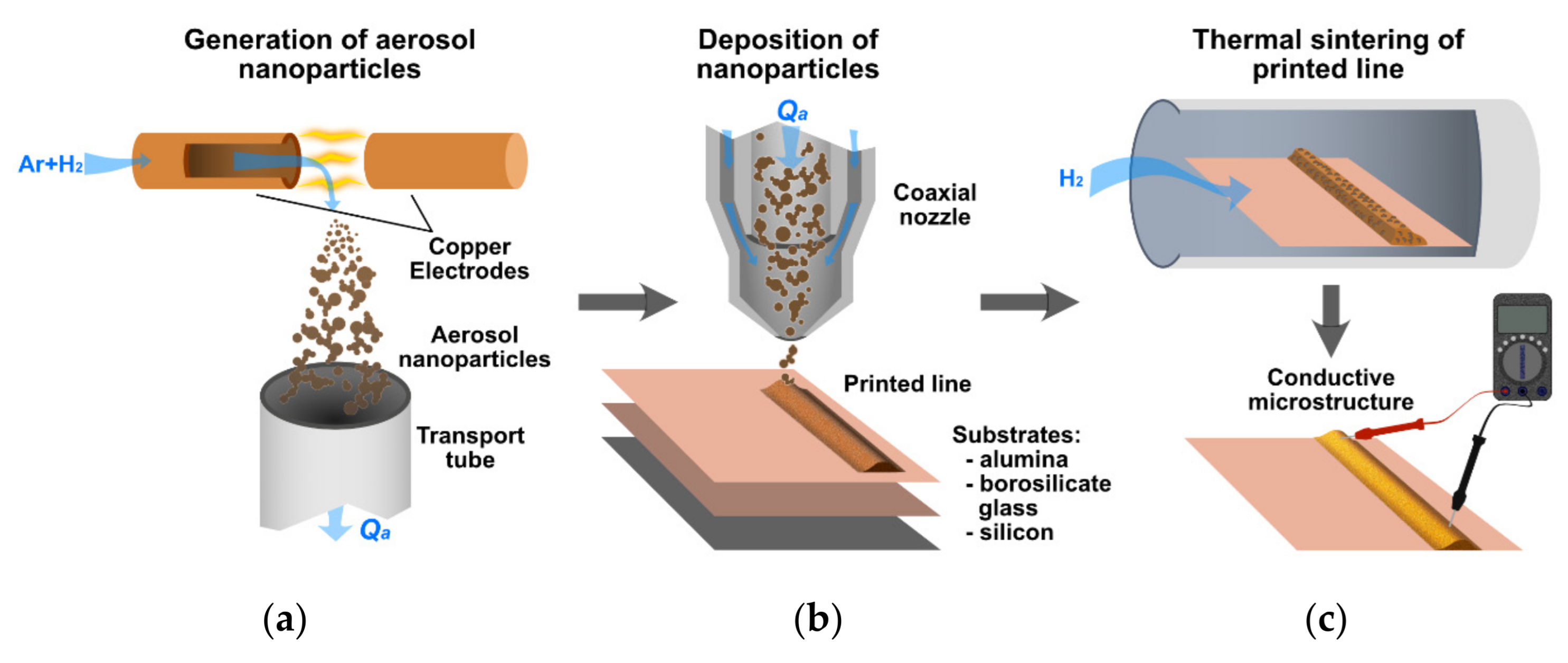
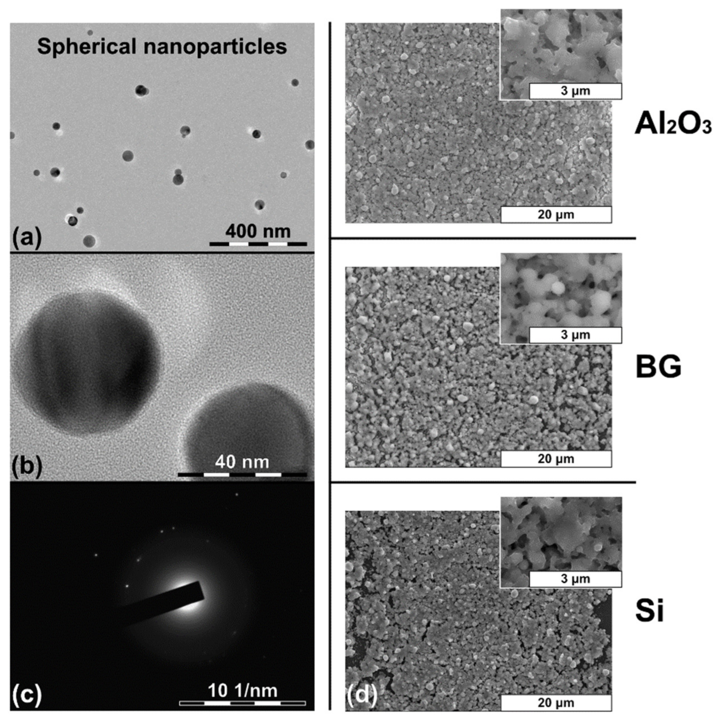
2. Materials and Methods

Figure 1 shows experiment scheme on the formation and thermal sintering of printed lines from nanoparticles on various substrates for fabricating current-carrying and gas-sensitive microstructures. The formation of printed lines with a width of 100–150 µm and a length of 1.5–2.0 mm was carried out due to the focused deposition of aerosol nanoparticles on moving substrates. Common materials in printed electronics, such as alumina Al2O3 (VK-100 ceramic, C-Component Ltd., Moscow, Russia), borosilicate glass BG (GETECH, Shenzhen, China), and silicon Si (Si-CZ, Microchemicals GmbH, Ulm, Germany), were used as substrates. Alumina and borosilicate glass are dielectrics and silicon has a resistivity equal to 1–10 Ω∙cm, which is several orders higher than the resistance of copper lines. Silicon also contained a natural dielectric layer of SiO2 on the surface with a thickness of several nanometers. In the experiments, the electrical and gas-sensitive characteristics of printed lines made of nanoparticles were investigated. Thermal sintering of lines to obtain conductive microstructures was carried out using a tube furnace in a hydrogen atmosphere. In turn, gas-sensitive microstructures, which are the original unsintered lines, were tested in the experimental setup “Mikrogaz-F” [24] for the detection of ammonia (NH3) and carbon monoxide (CO).
In the process of “dry” aerosol jet printing, nanoparticles were synthesized directly in a spark discharge due to electrical erosion of copper electrodes (Cu ≥ 99.90%, KUZOCM, JSC, Kamensk-Uralsky, Russia) in an argon-hydrogen flow (Ar 95% + H2 5%). This gas mixture was used as a reducing agent to limit the oxidation of nanoparticles during their synthesis. An optimized process for the synthesis of nanoparticles using a spark discharge was previously reported in works [25,26]. The size, morphology, and crystal structure of the synthesized nanoparticles were investigated using a transmission electron microscope (JEM-2100, JEOL Ltd., Tokyo, Japan). Real-time particle size distribution was measured using an aerosol spectrometer (SMPS 3936, TSI Inc., Shoreview, MN, USA). Further, aerosol nanoparticles were focused and deposited on substrates through a coaxial micro nozzle with an outlet diameter of 100 μm. Aerosol nanoparticles collided with the substrate at high speed (50–150 m/s) and attached to its surface due to the van der Waals force. The width of the nanoparticle beam was controlled by the flow rates of the carrier gas Qa and the sheath flow Qsh, respectively. At the same time, the sheath flow Qsh limited the expansion of the nanoparticle beam and protected the nozzle clogging. The focusing process of aerosol nanoparticles was described in more detail in the works [15,27,28]. In the presented experiments, Qa and Qsh were equal to 50 and 20 sccm, respectively. The distance from the nozzle to the substrate and the speed of substrate were 0.3 mm and 0.42 mm/min, respectively. The number of print layers varied from 2 to 5.
Thermal sintering of lines was used to reduce oxidized copper nanoparticles and obtain conductive copper microstructures. The printed lines were sintered at various temperatures ranging from 350 to 650 °C for 60 min using a tube furnace using H2 as a reducing agent at a flow rate of about 50 sccm. The length and internal diameter of the tube furnace chamber were 560 and 30 mm, respectively. The sample-heating rate was 5 °C/min with natural cooling in a controlled atmosphere. The electrical resistivity ρ of current-carrying microstructures was investigated depending on the sintering temperature Tsint and the type of substrate material. There were 5 lines on each type of substrate formed for each temperature sintering to define the accuracy. The electrical resistivity was determined by the following Equation (1):
ρ = R · A L
where R—electrical resistance; A—cross-sectional area; L—length.
Contact pads were formed at both ends of the lines using silver paste PELCO® (product No. 16031, Ted Pella, Inc., Redding, CA, USA) to measure their resistance after the sintering process. Silver paste solidified at room temperature, which excluded further heating of the sintered lines. The electrical resistance of the line R was measured using a multimeter (U1272A, Agilent Technologies Inc., Santa Clara, CA, USA). The cross-sectional area A and the length L of each of the five lines formed on the same type of substrate and sintered at the same temperature were independently measured by an optical 3D profilometer (S neox, Sensofar, Terrassa, Spain).
Wherein, the initial unsintered lines of nanoparticles were investigated as gas-sensitive microstructures. These lines were formed on a special alumina substrate containing a platinum heater and built-in electrodes for measuring the resistance of the gas-sensitive layer. The resistance of the gas-sensitive layer to the action of the target gases CO and NH3 mixed with air was measured using a controlled gas mixer “Mikrogaz-F” [24]. Synthetic air consisting of oxygen and nitrogen of high purity (99.999%) was used in the experiments. The “Mikrogaz-F” unit fed into the gas chamber the content of target gases in the concentration range from 1 to 50 ppm with controlled humidity in the air of 50% RH. The investigated range captured the threshold limits of values according to Russian Hygiene Norm [29]. For example, the threshold limit value of CO and NH3 is 17 ppm and 28 ppm, respectively. The mode of measuring the gas-sensitive characteristics of the original unsintered lines is presented in Table 1.
The microstructure and elemental composition of the printed lines were investigated using a scanning electron microscope SEM (JSM-7001F, JEOL Ltd., Tokyo, Japan) with an attachment for energy-dispersive X-ray (EDX) spectroscopy. The EDX analysis was performed by XFlash detector (6-30, Bruker Corporation, Billerica, MA, USA).

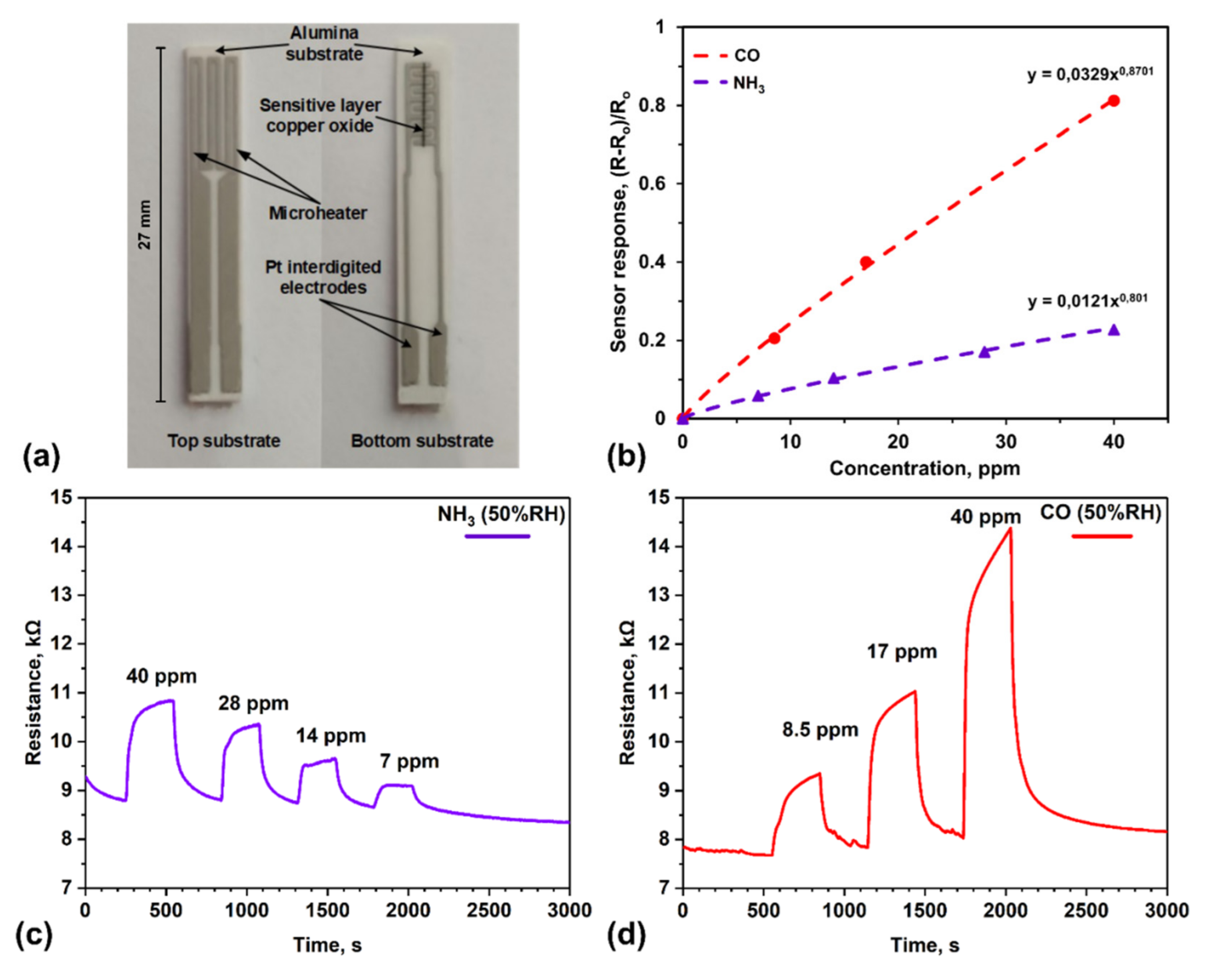
3. Results and Discussion

In the process of “dry” AJP, the synthesis of nanoparticles was carried out continuously as a result of a spark discharge between the electrodes. Thus, copper-based nanoparticles were obtained in the process of evaporation-condensation of electrodes in a controlled gas atmosphere [30]. Figure 2a,b shows the corresponding transmission electron microscopy (TEM) images of nanoparticles synthesized in a spark discharge by erosion of copper electrodes in an argon-hydrogen atmosphere (Ar 95% + H2 5%).
The figures show that the resulting nanoparticles are fractal-like agglomerates consisting of separate near-spherical primary nanoparticles [31]. The average size of primary nanoparticles is 10.8 ± 4.9 nm, according to the analysis of TEM images, see Figure 2c. In this case, according to measurements on an aerosol spectrometer, the mode size of the agglomerates is 98 ± 9 nm (Figure A2, Appendix A). These dimensions are typical for the synthesis of nanoparticles using a spark discharge [32]. Based on the results of the analysis of TEM images and the electron diffraction pattern, it was determined that the resulting nanoparticles have a crystalline structure with a small fraction of an amorphous oxide shell on the surface. The high-resolution TEM image (Figure 2b) shows that the thickness of the amorphous layer on the surface of the recently obtained nanoparticles is approximately 3–5 nm. The formation of an amorphous layer on the surface of nanoparticles can be associated with the process of oxidation of the samples during their exposure and storage in air. Earlier it was reported that copper nanoparticles synthesized by other gas-phase methods [33], also inevitably consist of an oxide shell layer that affects the conductivity of microstructures. The crystal structure of copper nanoparticles was determined by analyzing the electron diffraction pattern. As shown in Figure 2d, the electron diffraction pattern consists of rings corresponding to interplanar spacings of 2.06, 1.83, 1.26, and 1.09 Å. These values are in good agreement with the values characteristic of the (111), (200), (220), and (311) planes of pure copper without any impurities with a cubic face-centered unit cell and space group Fm3m [34].
Figure 3a–c shows the cross-sectional profiles of printed lines of copper-based nanoparticles formed on alumina, borosilicate glass, and silicon substrates, respectively. This figure shows that the line profiles have a similar Gaussian shape, a width of 100–150 µm and a height of 5–7 µm, regardless of the substrate material and the degree of their roughness. In this case, the broadening effect of the deposited material does not significantly appear, as, for example, in the case of inkjet or microplotter printing [35], since in the process of “dry” AJP, the formation of lines is carried out due to the direct deposition of nanoparticles on the substrate without the use of inks and solvents. This feature can be a key advantage when forming functional lines on different substrates over traditional “wet” printing processes.
As known, copper nanoparticles tend to oxidize easily under environmental conditions [33,34]. Printed lines based on copper nanoparticles synthesized in a spark discharge are no exception. From the analysis of the EDX spectra, it was found that the initial unsintered lines, stored in air for several days, have noticeable oxygen peaks at the level of 3–4 wt%, see Figure 3d. Due to the oxidation of nanoparticles, the initial lines had a high resistance at room temperature of 25 ± 5 °C equal to >300 MΩ, which is above the measurement limit by the multimeter used. In this case, the presence of zinc impurities in the samples is explained by the evaporation of brass holders during the synthesis of nanoparticles. Zinc impurity is also observed in platinum nanoparticles produced using a similar spark discharge generator with brass holders [36].
Based on the results of measurements of the temperature dependence of the resistance, it was determined that the initial lines of nanoparticles exhibit a semiconductor type of conductivity. Thus, the resistance of the samples decreased monotonically with an increase in their temperature in the range from room temperature to 300 °C (573 K) (Figure A1, Appendix A). This semiconducting character of conductivity indirectly indicates the presence of oxidized nanoparticles in the composition of printed lines, for example, CuO or Cu2O, which are typical metal oxide semiconductors [37]. Moreover, based on the results of gas-sensitive measurements, it was determined that unsintered lines demonstrate p-type conductivity, characteristic of CuO [37]. This type of conductivity is indirectly confirmed by an increase in the resistance of the unsintered line in the presence of a gas impurity (carbon monoxide and ammonia). It is known that the resistance increase in a concentrated gas environment occurs due to the formation of surface-active radicals exhibited by the dissociation of gas impurity molecules at heated oxide surfaces [10]. This leads to the formation of free electrons. The excessive free electrons appearing because of the surface reactions recombine with holes at p-type oxides reduces a free carrier concentration and thus increasing the resistance of the oxide [10].
It is known that the presence of surface oxides can be reduced by sintering nanoparticles in a reducing atmosphere [38]. Thus, with the aim of producing conductive microstructures, reductive sintering of the formed lines was performed. Sintering was carried out in a tube furnace with the length and internal diameter of the chamber 560 and 30 mm, respectively, in a hydrogen atmosphere with a gas flow rate of about 50 sccm. The gas flow was controlled at the inlet to the tube furnace using a mass gas flow regulator. The heating rate of the samples was 5 °C/min with holding at a given temperature of 350–650 °C for 60 min. Sintering of the lines at the furnace temperature of ≥750 °C led to the destruction of the lines and an increase in the resistivity, respectively. Based on the results of these experiments, the effect of the sintering temperature on the electrical resistivity, morphology, and elemental composition of printed lines was determined.
Figure 4 shows the change in the electrical resistivity of the lines ρ on various substrates depending on the sintering temperature Tsint, as well as their corresponding optical images. As the sintering temperature increases, the electrical resistivity of the lines decreases noticeably, and then reaches saturation, see Figure 4a. For example, the electrical resistivity approached its minimum value of 35–45 µΩ∙cm at a sintering temperature of about 650 °C.
Figure 4 also shows that reductive sintering of oxidized copper nanoparticles begins to be noticeable at sintering temperatures above 450 °C. At these temperatures, the lines become conductive (Figure 4a), and their color changes from black to red-orange (Figure 4b). Moreover, the oxygen concentration decreases from 3.0 to 0.5 wt% when the temperature Tsint increases from 350 °C to 450 °C, respectively. For example, the oxygen concentration in the unsintered lines was 3–5 wt%. The oxygen concentration is totally removed only at sintering temperatures above 550 °C according to EDX analysis. Thus, it was experimentally found that a temperature of 450 °C becomes sufficient to activate the chemical reaction of copper oxide reduction, according to the following expression: CuxO + H2(g) → xCu + H2O(g). The high temperature of reductive sintering of 450 °C is probably associated with a rather thick 3–5 nm oxide shell on the surface of the synthesized nanoparticles (see Figure 2b), since copper oxides have a higher melting point than metallic copper [39]. High sintering temperatures can limit the use of thermosensitive polymer substrates such as polyimide, polyethylene naphthalate, and others.
To explain the changes in electrical resistivity during reductive sintering, we additionally performed a microstructural analysis of the surface of lines sintered at different temperatures, the results of which are shown in Figure 5. Samples sintered at 350 °C were a typical fine-grained structure formed by a network of oxidized copper nanoparticles, see Figure 5a. Thereby, these samples had a high electrical resistivity, much more than 400 µΩ∙cm (see Figure 4a).
Figure 5b shows that the reduction sintering of the lines began at a temperature of 450 °C as a result of the coarsening of grains and a decrease in the porosity of the microstructure. Further compaction of the microstructure accelerated with an increase in temperature to 550 °C, as shown in Figure 5c. This condensation of the microstructure resulted in a sharp decrease in the electrical resistivity from 275 to 100 µΩ∙cm, see Figure 4a. At the same time, with an increase in the sintering temperature to 650 °C, the growth of microstructure compaction became less noticeable, and the sintered lines reached the minimum electrical resistivity at the level of 35–45 µΩ∙cm. It should be noted that high sintering temperatures of 650 °C could also lead to cracking and partial peeling of lines due to differences in the coefficients of thermal expansion of the particle and substrate materials. In this connection, it was experimentally found that the recommended sintering temperature should be reduced to 550 °C. At this temperature, the sintered lines have good adhesive strength and acceptable electrical resistivity.
From the results of elemental analysis (Figure 6a), measured by SEM, it was found that with an increase in the sintering temperature from 350 °C to 650 °C, there is a significant increase in the mass fraction of copper from 78.4 to 99.7 wt%, respectively. This increase is indicative of effective copper reduction with complete removal of oxides from sintered microstructures. Figure 6a shows that there is a zinc impurity in the samples. It is known that zinc oxide is also effectively reduced with hydrogen ZnO + H2 (g) → Zn (g) + H2O (g) [40] followed by complete evaporation of Zn at the temperature of 700 °C [41]. Probably, similar processes take place in our experiments.
However, despite the high proportion of copper, the electrical resistivity of the sintered lines is 10–15 times higher than the electrical resistivity of the bulk material ~1.7 µΩ∙cm. The main reason for this low resistance may be the large number of pores in the sintered lines. In the case of the presence of pores in the volume of the line, it can be difficult to understand the quality of their sintering, examining only the surface morphology. For this reason, additional studies on the degree of shrinkage S of the line depending on the sintering temperature were performed. The degree of shrinkage S of the line, which is responsible for the change in the cross-sectional area before and after sintering, was determined using the following Equation (2):
S = A 0 A A 0
where S, A0 and A are the shrinkage, cross-sectional areas of the initial and sintered lines, respectively.
Figure 6b shows, as an example, the change in the cross-sectional profile of a line on an alumina substrate at different reductive sintering temperatures. The general result of determining the degree of shrinkage of lines on substrates of Al2O3, BG, and Si, depending on the sintering temperature, is presented in Table 2 as the average value of measurements of five lines on one type of substrate for each sintering temperature.
The Table 2 shows that the degree of shrinkage of the lines after sintering at 350 °C is insignificant and amounts to 12–15%. At the same time, a significant shrinkage of the printed lines equal to 45–59% is observed with an increase in the sintering temperature to 450 °C, and reaches a maximum value of about 70% at a temperature of 650 °C. In this regard, it can be seen that the degree of shrinkage (Table 2) and electrical resistivity (Figure 4a) of the lines correlate with each other. Thus, incomplete shrinkage or high residual porosity of the samples can be the reason for their high electrical resistivity.
It is known from sintering theory that sintered agglomerate structures contain a large number of closed pores [42]. Considering this, additional experiments were performed on the formation and sintering of lines from spherical nanoparticles instead of fractal-like agglomerates in order to obtain denser and highly conductive microstructures. Spherical nanoparticles were produced using a spark discharge as shown in Figure 1, but the aerosol nanoparticles were additionally passed through a tube furnace prior to deposition onto a substrate. As a result of this heat treatment at 1000 °C for 6 s, the shape of aerosol particles was transformed from fractal-like agglomerates to spherical nanoparticles with a size of 20–50 nm, according to transmission electron microscopy, see Figure 7a–c. The transformation of the shape and size of aerosol nanoparticles using a tube furnace is described in detail in works [43].
After focused deposition and thermal sintering, the electrical resistivity, morphology, elemental composition and shrinkage of printed lines were also investigated. SEM images (Figure 7d) of lines from spherical nanoparticles sintered at Tsint = 550 °C show that they have a denser microstructure and fewer cracks, in contrast to lines from sintered agglomerates (Figure 5b). At the same time, the degree of shrinkage and the elemental composition of these lines were similar to structures of fractal-like agglomerates, see Table 2 and Table 3. The aspects related to the influence of agglomeration on the sintering result have been previously investigated in various works [42,44]. It is known that the agglomeration of nanoparticles, in general, reduces the density of the sintered microstructure [42]. Agglomeration refers to the assemblage of two or more primary nanoparticles held together by the van der Waals force [45]. The presence of bonds between nanoparticles prevents their displacement during the compaction process, and as a result, dense packing of the microstructure is not achieved. Moreover, the packing density decreases with decreasing nanoparticle size due to an increase in interparticle interaction [42].
It can be seen from the results of TEM images that the initial aerosol nanoparticles are highly agglomerated, since they consist of many primary nanoparticles (Figure 2a). At the same time, aerosol nanoparticles passed through the tube furnace are mainly single spherical nanoparticles (Figure 7a). According to the results of measurements on an aerosol spectrometer, it can be seen that the modal sizes of the initial agglomerates are larger than the sizes of nanoparticles that have passed through the tube furnace—98 ± 9 nm and 62 ± 7 nm, respectively (Figure A2, Appendix A). Based on early research [44], it is expected that sintered lines formed from non-agglomerated spherical nanoparticles will have lower porosity (high density), and low resistivity compared to structures formed from the initial agglomerates. This assumption is confirmed by the results of measurements of the surface morphology and electrical resistivity of the sintered lines. Figure 7d and Figure 5c of the surfaces of sintered lines show qualitatively that lines from spherical nanoparticles have lower porosity than lines from initial agglomerates. Moreover, the resistivity of lines from spherical nanoparticles ~5 µΩ∙cm (Table 3) is noticeably lower than the resistivity of lines from initial agglomerates 70–100 µΩ∙cm (Figure 4), sintered at 550 °C. High residual porosity and high electrical resistivity of printed lines from initial agglomerates are associated with their high degree of agglomeration. It is known that agglomeration is the cause of the appearance of a bimodal porous structure with large inter-agglomerate and small intra-agglomerate pores [46], respectively. During sintering, small intra-agglomerate pores shrink faster than larger ones due to the higher local curvature. Thus, large inter-agglomerate pores are more difficult to remove [46]. Consequently, agglomeration leads to residual voids and inhomogeneous microstructure during the sintering process.
The electrical resistivity of the lines made of spherical nanoparticles was minimal and amounted to 5 µΩ∙cm (Table 3), which is approximately three times higher than that of bulk copper. These printed lines also showed long-term stability up to 2 months of storage in the environment without any significant reduction in electrical resistivity. At the same time, the achieved values of resistances of printed lines are comparable with competing methods based on the use of nano-ink. For example, at work [33] it was reported that arc discharge inkjet nano-ink had a resistivity of 5.4 ± 0.6 μΩ∙cm at a sintering temperature of 300 °C. Thus, it has been experimentally shown that the method of “dry” aerosol jet printing followed by sintering can be used to create conductive copper lines from spherical nanoparticles with excellent electrical properties on various substrates.
As defined above, the high porosity of loose agglomerate printed lines is an obstacle to the fabrication of highly conductive microstructures. In turn, highly porous microstructures from agglomerates can be promising for gas sensor applications, where a high specific surface area of a gas sensitive material is important. Thus, in this work, using the method of “dry” AJP, a gas-sensitive layer was formed on a measuring substrate made of alumina. The gas-sensitive layer based on copper nanoparticles was a low (less than 5 μm) printed line with a width of about 150 μm, deposited on the measuring electrodes, heated from below using a platinum heater in the form of a meander, see Figure 8a. Further, the formed structure was tested using the “Mikrogaz-F” gas-mixing system for the detection of gaseous impurities of ammonia and carbon monoxide, see Table 1. Based on the test results, the dependences of the resistance of the gas-sensitive layer on the concentration of NH3 and CO were determined; see Figure 8b–d.
The resistance of the sensors is decreased with increase of the working temperature, suggesting that the gas-sensitive layer possess characteristics of semiconductors. Figure 8c,d show the sensor response to NH3 and CO, correspondingly, at the working temperature of 270 °C. The increase of resistance under influence of the target gases is related to the sensing mechanism of p-type metal oxide semiconductors [47]. The chemical reaction between the target gases and surface oxygen removes the chemisorbed oxygen molecules releasing free electrons. In case of p-type copper oxide, release of electrons leads to recombination between holes and electrons, decrease of number of free holes, increase of potential barriers between nanoparticles and the corresponding increase in the resistance. The dependences of the relative change of resistance on the concentration of NH3 and CO gases are shown in Figure 8b. These dependencies can be fitted by a power law as usual for metal oxide sensors [48]. Figure 8c,d presents the resistance transients upon exposure to NH3 and carbon oxide. The observed response and recovery times (250–300 s) agree well with those reported in [37]. Response of the sensor fabricated based on non-sintered oxidized copper nanoparticles to ammonia and carbon monoxide concentration of 40 ppm is about 20% and 80%, respectively. Thus, the applicability of printed lines made of loose agglomerates based on oxidized copper as a sensitive layer of a gas sensor has been demonstrated.

4. Conclusions

The new method of “dry” aerosol jet printing, including the synthesis of nanoparticles by spark discharge, has prospects in the production of printed electronics products due to the absence of the need to prepare nano-ink, the simplicity, and versatility of the spectrum of the obtained nanomaterials (metals and their oxides, semiconductors and carbon). In this work, we have demonstrated the compatibility of this method with substrates made of various inorganic materials, such as alumina, borosilicate glass, and silicon. It was found that the broadening effect of the formed lines on various substrates practically does not appear in comparison with traditional approaches of “wet” printing. Depending on the conditions of post-printed heat treatment, both metallic and semiconducting (gas-sensitive) microstructures based on copper nanoparticles can be easily obtained. Sintering of copper oxide nanoparticles begins at the temperature of 450 °C in hydrogen atmosphere with the shrinkage of 45–60%. Copper lines based on spherical nanoparticles show a low electrical resistivity of 5 µΩ∙cm after reduction sintering at 550 °C for 60 min. In turn, semiconductor micro-structures based on unsintered agglomerates of oxidized copper have a fairly high sensitivity to NH3 and CO. Response of the sensor fabricated based on non-sintered oxidized copper nanoparticles to ammonia and carbon monoxide concentration of 40 ppm is about 20% and 80%, respectively.

Author Contributions

Conceptualization, A.A.E.; methodology, D.V.K. and A.I.B.; investigation, E.I.K., N.B.P., A.V.N., and A.E.V.; data curation, A.I.B., D.V.K., and P.V.A.; writing—original draft preparation, D.V.K.; writing—review and editing, A.A.E.; visualization, A.A.L.; project administration, A.A.E. and V.V.I. All authors have read and agreed to the published version of the manuscript.

Funding

This work was supported by the Russian Science Foundation (project no. 19-79-00375).

Institutional Review Board Statement

Not applicable.

Informed Consent Statement

Not applicable.

Data Availability Statement

The data presented in this study are available upon request from the corresponding author.

Conflicts of Interest

The authors declare no conflict of interest.

Appendix A

Figure A1. Temperature dependence on resistance of the unsintered line for determination of type conductivity.
Applsci 11 05791 g0a1
Figure A2. Particle size distributions of agglomerates and spherical NPs measured at the outlet of the coaxial micro nozzle by the aerosol spectrometer (SMPS 3936, TSI Inc., Shoreview, MN, USA). FWHM is the full width at half maximum.
Applsci 11 05791 g0a2

References

  1. Kassem, O.; Saadaoui, M.; Rieu, M.; Viricelle, J.-P. A Novel Approach to a Fully Inkjet Printed SnO2-Based Gas Sensor on a Flexible Foil. J. Mater. Chem. C 2019, 7, 12343–12353. [Google Scholar] [CrossRef]
  2. Singh, R.; Singh, E.; Nalwa, H.S. Inkjet Printed Nanomaterial Based Flexible Radio Frequency Identification (RFID) Tag Sensors for the Internet of Nano Things. RSC Adv. 2017, 7, 48597–48630. [Google Scholar] [CrossRef] [Green Version]
  3. Han, G.D.; Bae, K.; Kang, E.H.; Choi, H.J.; Shim, J.H. Inkjet Printing for Manufacturing Solid Oxide Fuel Cells. ACS Energy Lett. 2020, 5, 1586–1592. [Google Scholar] [CrossRef]
  4. Zhu, H.; Shin, E.-S.; Liu, A.; Ji, D.; Xu, Y.; Noh, Y.-Y. Printable Semiconductors for Backplane TFTs of Flexible OLED Displays. Adv. Funct. Mater. 2020, 30, 1904588. [Google Scholar] [CrossRef]
  5. Wu, C.-J.; Sheng, Y.-J.; Tsao, H.-K. Copper Conductive Lines on Flexible Substrates Fabricated at Room Temperature. J. Mater. Chem. C 2016, 4, 3274–3280. [Google Scholar] [CrossRef]
  6. Arsenov, P.V.; Efimov, A.A.; Ivanov, V.V. Optimizing Aerosol Jet Printing Process of Platinum Ink for High-Resolution Conductive Microstructures on Ceramic and Polymer Substrates. Polymers 2021, 13, 918. [Google Scholar] [CrossRef]
  7. Nayak, L.; Mohanty, S.; Nayak, S.K.; Ramadoss, A. A Review on Inkjet Printing of Nanoparticle Inks for Flexible Electronics. J. Mater. Chem. C 2019, 7, 8771–8795. [Google Scholar] [CrossRef]
  8. Wilkinson, N.J.; Smith, M.A.A.; Kay, R.W.; Harris, R.A. A Review of Aerosol Jet Printing—a Non-Traditional Hybrid Process for Micro-Manufacturing. Int. J. Adv. Manuf. Technol. 2019. [Google Scholar] [CrossRef] [Green Version]
  9. Suikkola, J.; Björninen, T.; Mosallaei, M.; Kankkunen, T.; Iso-Ketola, P.; Ukkonen, L.; Vanhala, J.; Mäntysalo, M. Screen-Printing Fabrication and Characterization of Stretchable Electronics. Sci. Rep. 2016, 6, 25784. [Google Scholar] [CrossRef] [PubMed]
  10. Fedorov, F.S.; Simonenko, N.P.; Trouillet, V.; Volkov, I.A.; Plugin, I.A.; Rupasov, D.P.; Mokrushin, A.S.; Nagornov, I.A.; Simonenko, T.L.; Vlasov, I.S.; et al. Microplotter-Printed On-Chip Combinatorial Library of Ink-Derived Multiple Metal Oxides as an “Electronic Olfaction” Unit. ACS Appl. Mater. Interfaces 2020, 12, 56135–56150. [Google Scholar] [CrossRef]
  11. Gao, D.; Zhou, J. Designs and Applications of Electrohydrodynamic 3D Printing. Int. J. Bioprinting 2019, 5. [Google Scholar] [CrossRef] [PubMed]
  12. Wegner, K.; Vinati, S.; Piseri, P.; Antonini, A.; Zelioli, A.; Barborini, E.; Ducati, C.; Milani, P. High-Rate Production of Functional Nanostructured Films and Devices by Coupling Flame Spray Pyrolysis with Supersonic Expansion. Nanotechnology 2012, 23, 185603. [Google Scholar] [CrossRef]
  13. Kim, H.; Kim, J.; Yang, H.; Suh, J.; Kim, T.; Han, B.; Kim, S.; Kim, D.S.; Pikhitsa, P.V.; Choi, M. Parallel Patterning of Nanoparticles via Electrodynamic Focusing of Charged Aerosols. Nat. Nanotechnol. 2006, 1, 117–121. [Google Scholar] [CrossRef]
  14. Lee, G.-Y.; Park, J.-I.; Kim, C.-S.; Yoon, H.-S.; Yang, J.; Ahn, S.-H. Aerodynamically Focused Nanoparticle (AFN) Printing: Novel Direct Printing Technique of Solvent-Free and Inorganic Nanoparticles. ACS Appl. Mater. Interfaces 2014, 6, 16466–16471. [Google Scholar] [CrossRef]
  15. Efimov, A.A.; Potapov, G.N.; Nisan, A.V.; Ivanov, V.V. Controlled Focusing of Silver Nanoparticles Beam to Form the Microstructures on Substrates. Results Phys. 2017, 7, 440–443. [Google Scholar] [CrossRef]
  16. Aghajani, S.; Accardo, A.; Tichem, M. Aerosol Direct Writing and Thermal Tuning of Copper Nanoparticle Patterns as Surface-Enhanced Raman Scattering Sensors. ACS Appl. Nano Mater. 2020, 3, 5665–5675. [Google Scholar] [CrossRef]
  17. Khabarov, K.; Kornyushin, D.; Masnaviev, B.; Tuzhilin, D.; Saprykin, D.; Efimov, A.; Ivanov, V. The Influence of Laser Sintering Modes on the Conductivity and Microstructure of Silver Nanoparticle Arrays Formed by Dry Aerosol Printing. Appl. Sci. 2020, 10, 246. [Google Scholar] [CrossRef] [Green Version]
  18. Meuller, B.O.; Messing, M.E.; Engberg, D.L.J.; Jansson, A.M.; Johansson, L.I.M.; Norlén, S.M.; Tureson, N.; Deppert, K. Review of Spark Discharge Generators for Production of Nanoparticle Aerosols. Aerosol Sci. Technol. 2012, 46, 1256–1270. [Google Scholar] [CrossRef]
  19. Teo, B.H.; Khanna, A.; Shanmugam, V.; Aguilar, M.L.O.; Delos Santos, M.E.; Chua, D.J.W.; Chang, W.-C.; Mueller, T. Development of Nanoparticle Copper Screen Printing Pastes for Silicon Heterojunction Solar Cells. Sol. Energy 2019, 189, 179–185. [Google Scholar] [CrossRef]
  20. Norita, S.; Kumaki, D.; Kobayashi, Y.; Sato, T.; Fukuda, K.; Tokito, S. Inkjet-Printed Copper Electrodes Using Photonic Sintering and Their Application to Organic Thin-Film Transistors. Org. Electron. 2015, 25, 131–134. [Google Scholar] [CrossRef] [Green Version]
  21. Li, W.; Zhang, H.; Gao, Y.; Jiu, J.; Li, C.-F.; Chen, C.; Hu, D.; Goya, Y.; Wang, Y.; Koga, H.; et al. Highly Reliable and Highly Conductive Submicron Cu Particle Patterns Fabricated by Low Temperature Heat-Welding and Subsequent Flash Light Sinter-Reinforcement. J. Mater. Chem. C 2017, 5, 1155–1164. [Google Scholar] [CrossRef]
  22. Rizwan, M.; Kutty, A.A.; Kgwadi, M.; Drysdale, T.D.; Sydänheimo, L.; Ukkonen, L.; Virkki, J. Possibilities of Fabricating Copper-Based RFID Tags With Photonic-Sintered Inkjet Printing and Thermal Transfer Printing. IEEE Antennas Wirel. Propag. Lett. 2017, 16, 1828–1831. [Google Scholar] [CrossRef] [Green Version]
  23. Li, W.; Sun, Q.; Li, L.; Jiu, J.; Liu, X.-Y.; Kanehara, M.; Minari, T.; Suganuma, K. The Rise of Conductive Copper Inks: Challenges and Perspectives. Appl. Mater. Today 2020, 18, 100451. [Google Scholar] [CrossRef]
  24. Yablokov, M.; Vasiliev, A.; Varfolomeev, A.; Zavyalov, S. Room Temperature Gas Multisensor System Based on a Novel Polymer Nanocomposite Material. Procedia Eng. 2014, 87, 152–155. [Google Scholar] [CrossRef] [Green Version]
  25. Mylnikov, D.; Efimov, A.; Ivanov, V. Measuring and Optimization of Energy Transfer to the Interelectrode Gaps during the Synthesis of Nanoparticles in a Spark Discharge. Aerosol Sci. Technol. 2019, 1393–1403. [Google Scholar] [CrossRef]
  26. Khabarov, K.; Urazov, M.; Lizunova, A.; Kameneva, E.; Efimov, A.; Ivanov, V. Influence of Ag Electrodes Asymmetry Arrangement on Their Erosion Wear and Nanoparticle Synthesis in Spark Discharge. Appl. Sci. 2021, 11, 4147. [Google Scholar] [CrossRef]
  27. Binder, S.; Glatthaar, M.; Rädlein, E. Analytical Investigation of Aerosol Jet Printing. Aerosol Sci. Technol. 2014, 48, 924–929. [Google Scholar] [CrossRef] [Green Version]
  28. Secor, E.B. Principles of Aerosol Jet Printing. Flex. Print. Electron. 2018, 3, 035002. [Google Scholar] [CrossRef]
  29. On the Approval of Sanitary Rules and Norms SanPiN 1.2.3685-21 “Hygienic Norms and Requirements for Ensuring Safety and (Or) Harmlessness for Human Environmental Factors”—Docs.Cntd.Ru. Available online: https://docs.cntd.ru/document/573500115 (accessed on 10 June 2021).
  30. Ivanov, V.V.; Efimov, A.A.; Myl’nikov, D.A.; Lizunova, A.A. Synthesis of Nanoparticles in a Pulsed-Periodic Gas Discharge and Their Potential Applications. Russ. J. Phys. Chem. A 2018, 92, 607–612. [Google Scholar] [CrossRef]
  31. Goudeli, E. Chapter 4—Formation and growth of fractal-like agglomerates and aggregates in the gas phase. In Frontiers of Nanoscience; Computational Modelling of Nanomaterials; Grammatikopoulos, P., Ed.; Elsevier: London, UK, 2020; Volume 17, pp. 41–60. [Google Scholar]
  32. Lizunova, A.A.; Efimov, A.A.; Arsenov, P.V.; Ivanov, V.V. Influence of the Sintering Temperature on Morphology and Particle Size of Silver Synthesized by Spark Discharge. IOP Conf. Ser. Mater. Sci. Eng. 2018, 307, 012081. [Google Scholar] [CrossRef]
  33. Fu, Q.; Stein, M.; Li, W.; Zheng, J.; Kruis, F.E. Conductive Films Prepared from Inks Based on Copper Nanoparticles Synthesized by Transferred Arc Discharge. Nanotechnology 2019, 31, 025302. [Google Scholar] [CrossRef] [PubMed]
  34. Kim, C.; Lee, G.; Rhee, C.; Lee, M. Expeditious Low-Temperature Sintering of Copper Nanoparticles with Thin Defective Carbon Shells. Nanoscale 2015, 7, 6627–6635. [Google Scholar] [CrossRef] [PubMed]
  35. Beedasy, V.; Smith, P.J. Printed Electronics as Prepared by Inkjet Printing. Materials 2020, 13, 704. [Google Scholar] [CrossRef] [PubMed] [Green Version]
  36. Efimov, A.A.; Arsenov, P.V.; Borisov, V.I.; Buchnev, A.I.; Lizunova, A.A.; Kornyushin, D.V.; Tikhonov, S.S.; Musaev, A.G.; Urazov, M.N.; Shcherbakov, M.I.; et al. Synthesis of Nanoparticles by Spark Discharge as a Facile and Versatile Technique of Preparing Highly Conductive Pt Nano-Ink for Printed Electronics. Nanomaterials 2021, 11, 234. [Google Scholar] [CrossRef]
  37. Rydosz, A. The Use of Copper Oxide Thin Films in Gas-Sensing Applications. Coatings 2018, 8, 425. [Google Scholar] [CrossRef] [Green Version]
  38. Kim, I.; Kim, J. The Effect of Reduction Atmospheres on the Sintering Behaviors of Inkjet-Printed Cu Interconnectors. J. Appl. Phys. 2010, 108, 102807. [Google Scholar] [CrossRef]
  39. Magdassi, S.; Grouchko, M.; Kamyshny, A. Copper Nanoparticles for Printed Electronics: Routes Towards Achieving Oxidation Stability. Materials 2010, 3, 4626–4638. [Google Scholar] [CrossRef] [Green Version]
  40. Reisman, A.; Berkenblit, M.; Ghez, R.; Chan, S.A. The Equilibrium Constant for the Reaction of ZnO + H2 and the Chemical Vapor Transport of Zno via the Zn + H2O Reaction. J. Electron. Mater. 1972, 1, 395–419. [Google Scholar] [CrossRef]
  41. Qi, J.; Hu, X. The Loss of ZnO as the Support for Metal Catalysts by H2 Reduction. Phys. Chem. Chem. Phys. 2020, 22, 3953–3958. [Google Scholar] [CrossRef]
  42. German, R.M. Chapter Thirteen—Nanoscale Sintering. In Sintering: From Empirical Observations to Scientific Principles; German, R.M., Ed.; Butterworth-Heinemann: Boston, MA, USA, 2014; pp. 413–432. ISBN 978-0-12-401682-8. [Google Scholar]
  43. Kornyushin, D.V.; Efimov, A.A.; Khabarov, K.M.; Ivanov, V.V. The Influence of the Morphology of Oxidized Copper Nanoparticles on the Electrical Properties of Microstructures Obtained by Dry Aerosol Printing. J. Phys. Conf. Ser. 2020, 1695, 012032. [Google Scholar] [CrossRef]
  44. Ragulya, A.V. Consolidation of Ceramic Nanopowders. Adv. Appl. Ceram. 2008, 107, 118–134. [Google Scholar] [CrossRef]
  45. Ferkel, H.; Hellmig, R.J. Effect of Nanopowder Deagglomeration on the Densities of Nanocrystalline Ceramic Green Bodies and Their Sintering Behaviour. Nanostruct. Mater. 1999, 11, 617–622. [Google Scholar] [CrossRef]
  46. Giuntini, D.; Bordia, R.K.; Olevsky, E.A. Feasibility of in Situ De-Agglomeration during Powder Consolidation. J. Am. Ceram. Soc. 2019, 102, 628–643. [Google Scholar] [CrossRef]
  47. Steinhauer, S. Gas Sensors Based on Copper Oxide Nanomaterials: A Review. Chemosensors 2021, 9, 51. [Google Scholar] [CrossRef]
  48. Lin, T.; Lv, X.; Hu, Z.; Xu, A.; Feng, C. Semiconductor Metal Oxides as Chemoresistive Sensors for Detecting Volatile Organic Compounds. Sensors 2019, 19, 233. [Google Scholar] [CrossRef] [PubMed] [Green Version]
Figure 1. Scheme of the formation of printed lines from nanoparticles on various substrates, including (a) generation, (b) focused deposition, and (c) thermal sintering processes.
Applsci 11 05791 g001
Figure 2. (a,b) TEM images of nanoparticles synthesized in a spark discharge by erosion of copper electrodes in an argon atmosphere with hydrogen (Ar 95% + H2 5%) and the corresponding (c) particle size distribution and (d) electron diffraction pattern.
Applsci 11 05791 g002
Figure 3. Cross-sectional profiles of printed lines from nanoparticle formed on substrates of (a) alumina, (b) borosilicate glass, and (c) silicon, (d) typical energy-dispersive X-ray spectroscopy EDX-spectrum of presented lines measured by SEM JSM-7001F.
Applsci 11 05791 g003
Figure 4. (a) Values of electrical resistivity and (b) corresponding optical images of printed lines on substrates of Al2O3, BG, and Si, depending on the reduction sintering temperature of 350–650 °C.
Applsci 11 05791 g004
Figure 5. Scanning electron microscope (SEM) images of the surface of printed lines made of nanoparticles on alumina, borosilicate glass, and silicon substrates sintered in a reducing atmosphere at temperatures equal to (a) 350, (b) 450, (c) 550, and (d) 650 °C, respectively.
Applsci 11 05791 g005
Figure 6. (a) Changes in the elemental composition (results of EDX analysis) and (b) the cross-sectional profile of lines based on copper nanoparticles with the temperature of reductive on alumina substrate as an example.
Applsci 11 05791 g006
Figure 7. (a,b) TEM image of spherical nanoparticles obtained during heat treatment of agglomerates; and (c) corresponding electron diffraction pattern. (d) SEM images of printed lines of spherical nanoparticles on Al2O3, BG, and Si substrates sintered in a reducing hydrogen atmosphere at Tsint = 550 °C.
Applsci 11 05791 g007
Figure 8. (a) Photo of a microstructure in the form of a printed line based on nanoparticles of copper oxide formed on alumina substrate for gas sensor testing. (b) Dependence of the relative changes in resistance and (c,d) the corresponding time responses of the gas sensitive layer on the concentration of NH3 and CO.
Applsci 11 05791 g008
Table 1. The mode of measuring the gas-sensitive characteristics of the initial unsintered lines using the “Mikrogaz-F” gas mixing system.
Working Temperature, °CTarget GasConcentration, ppmRelative Humidity, %
270CO8.5, 17 and 4050
NH37, 14, 28 and 40
Table 2. Shrinkage of printed lines as a function of sintering temperature on various substrates.
Sintering Temperature Tsint, °CAlumina (Al2O3)Borosilicate Glass (BG)Silicon (Si)
Shrinkage S, %
35015 ± 712 ± 714 ± 7
45045 ± 859 ± 854 ± 6
55048 ± 565 ± 761 ± 7
65059 ± 669 ± 963 ± 8
Table 3. Electrical resistivity, shrinkage, and elemental composition of sintered lines made of spherical copper-based nanoparticles.
Alumina (Al2O3)Borosilicate Glass (BG)Silicon (Si)
Electrical resistivity ρ, µΩ·cm5.1 ± 0.65.3 ± 0.75.1 ± 0.8
Shrinkage S, %44 ± 1038 ± 932 ± 8
Elemental composition of sintered lines, wt.% Cu—98.6
Ag—1.0
O—0.4
Publisher’s Note: MDPI stays neutral with regard to jurisdictional claims in published maps and institutional affiliations.

