
Terahertz Photoconductive Antenna Based on a Topological Insulator Nanofilm


Abstract
1. Introduction
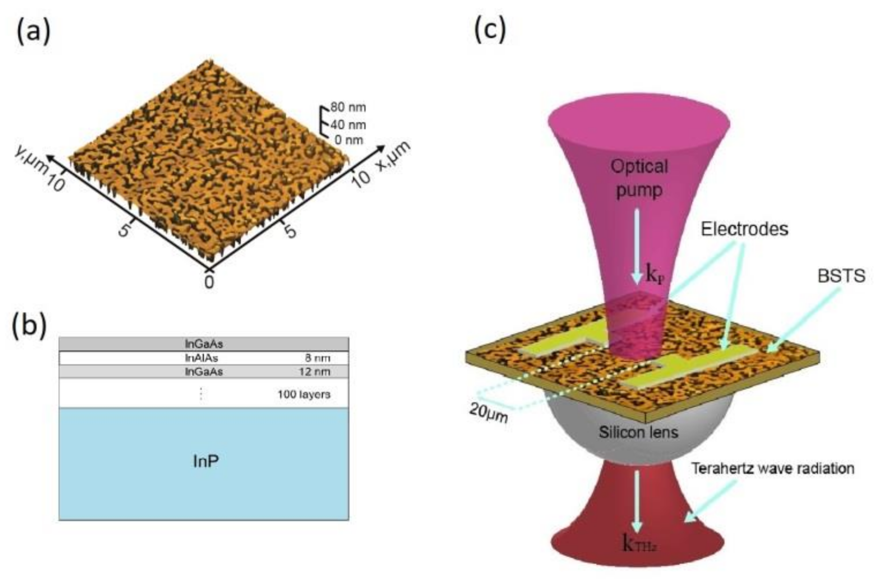
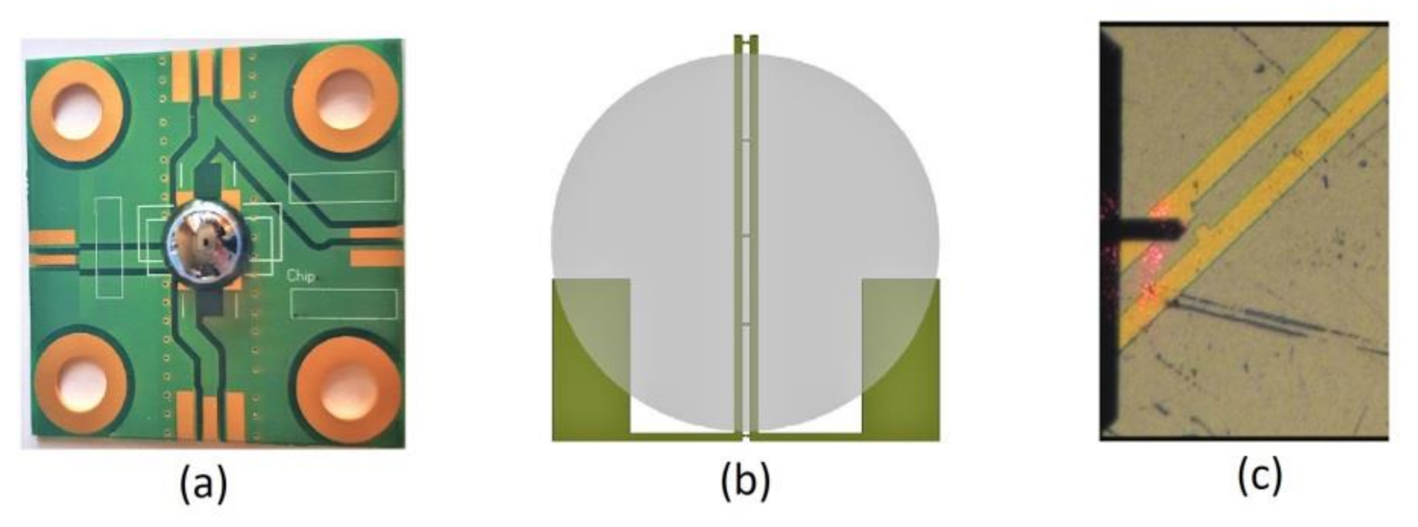
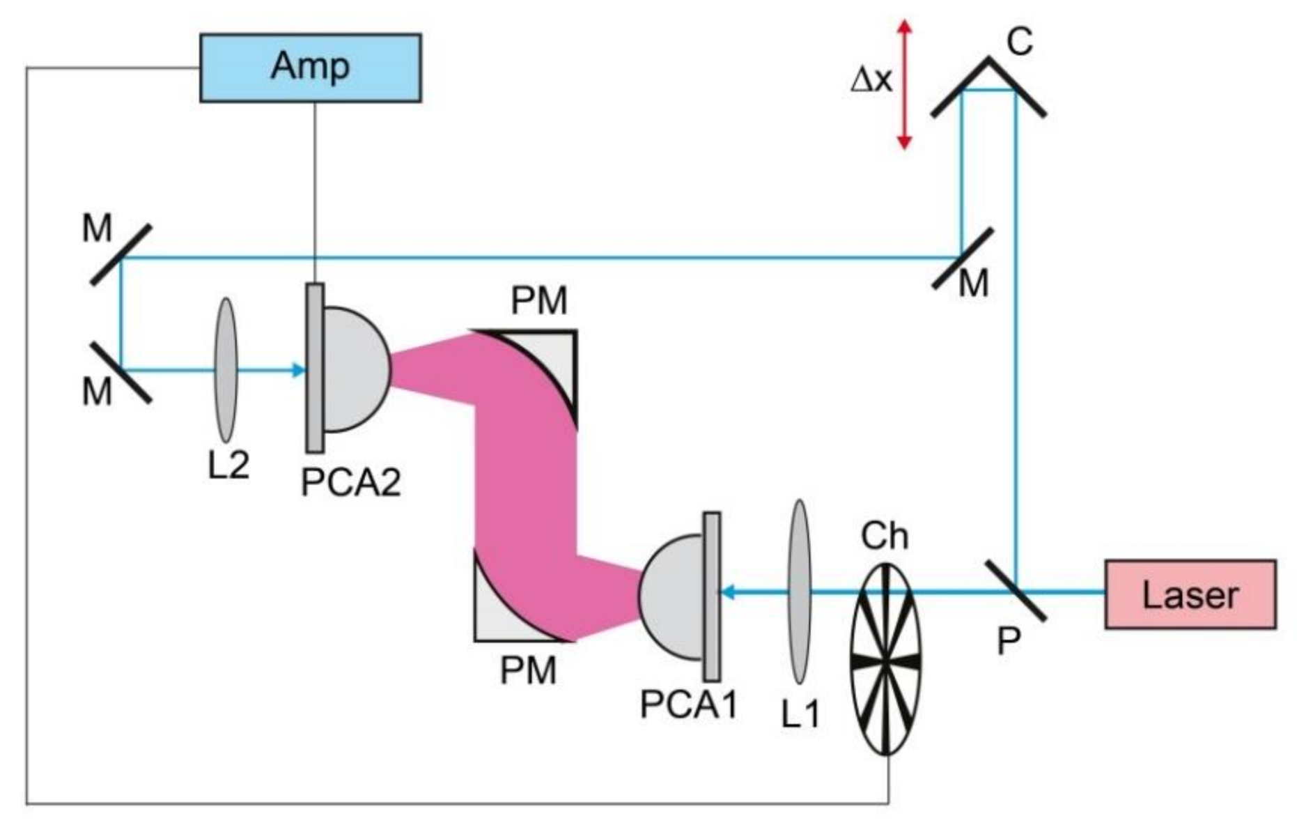
2. Proposed System Design
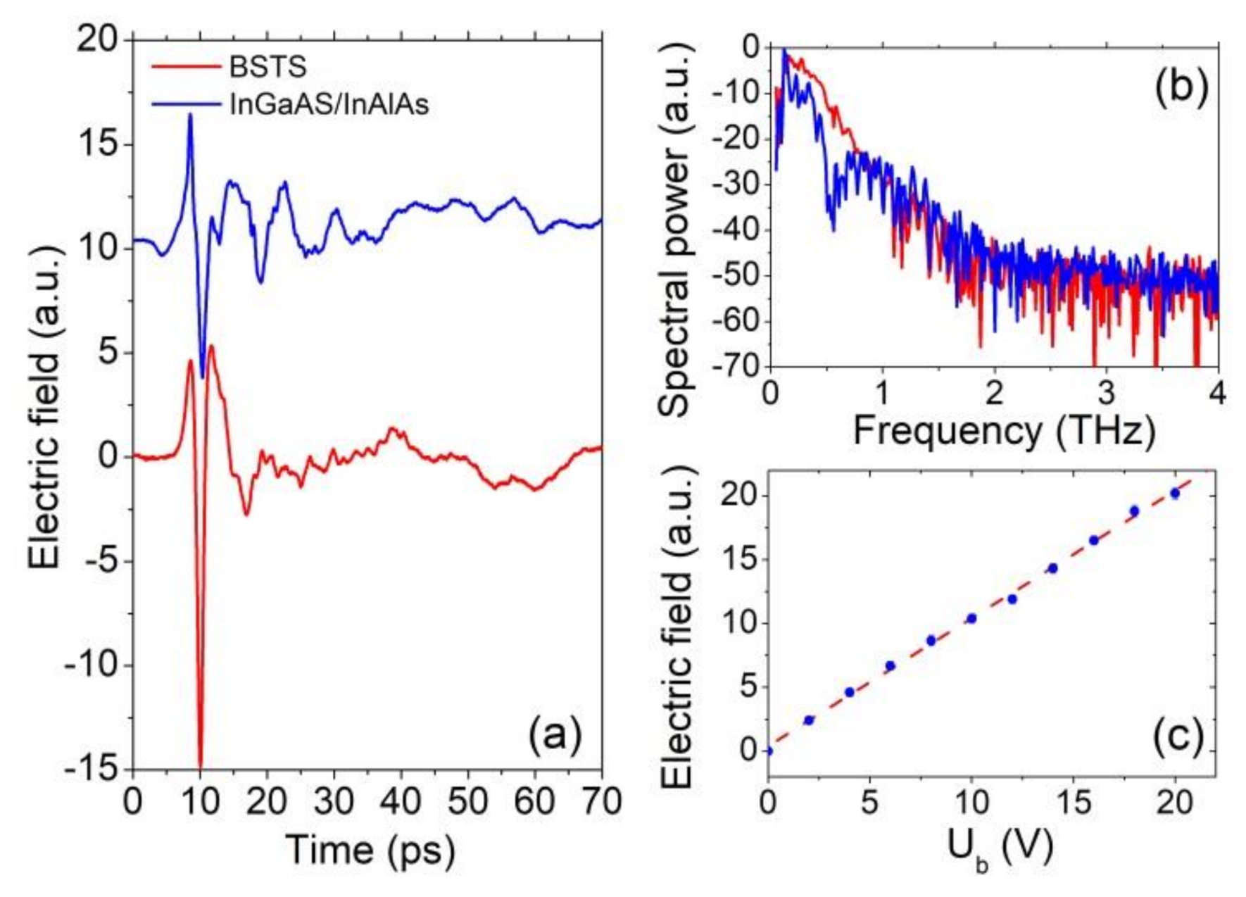
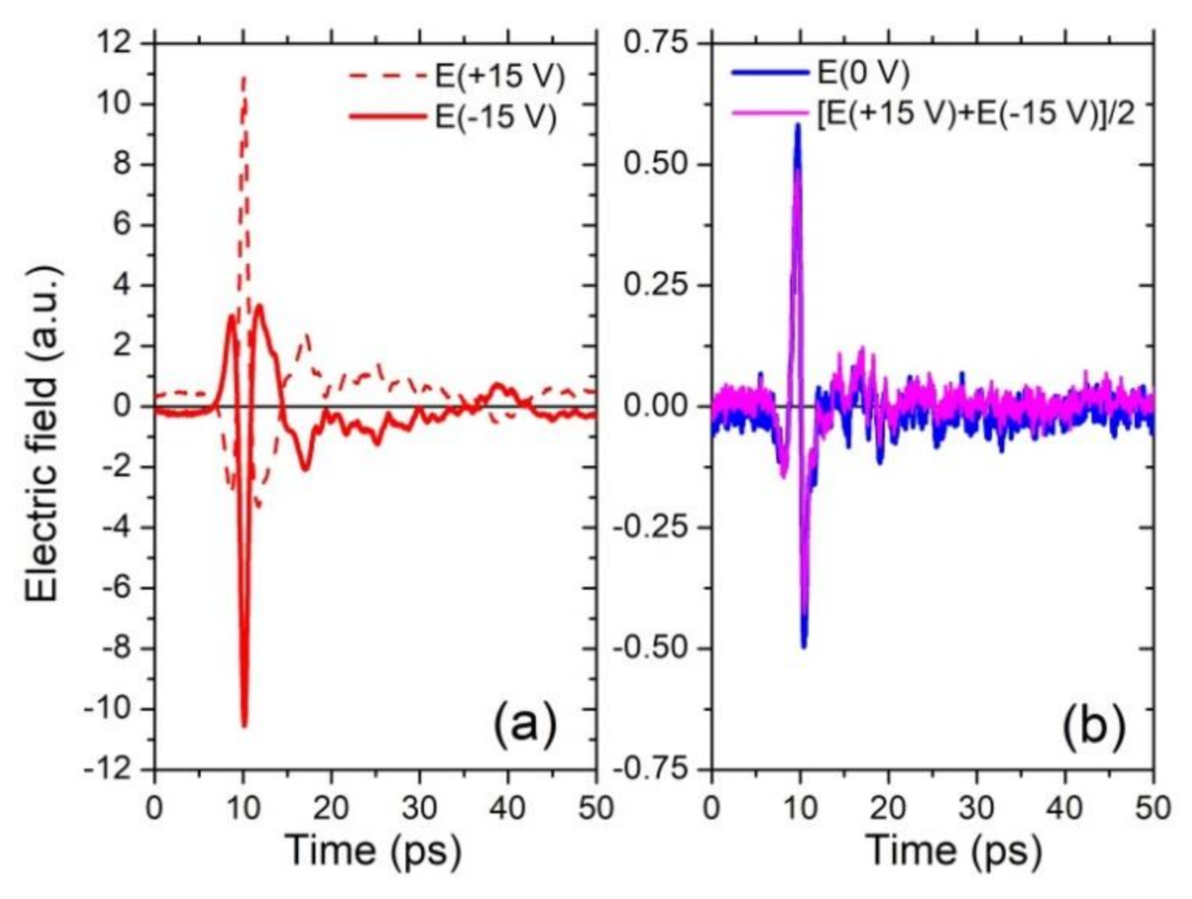
3. Results
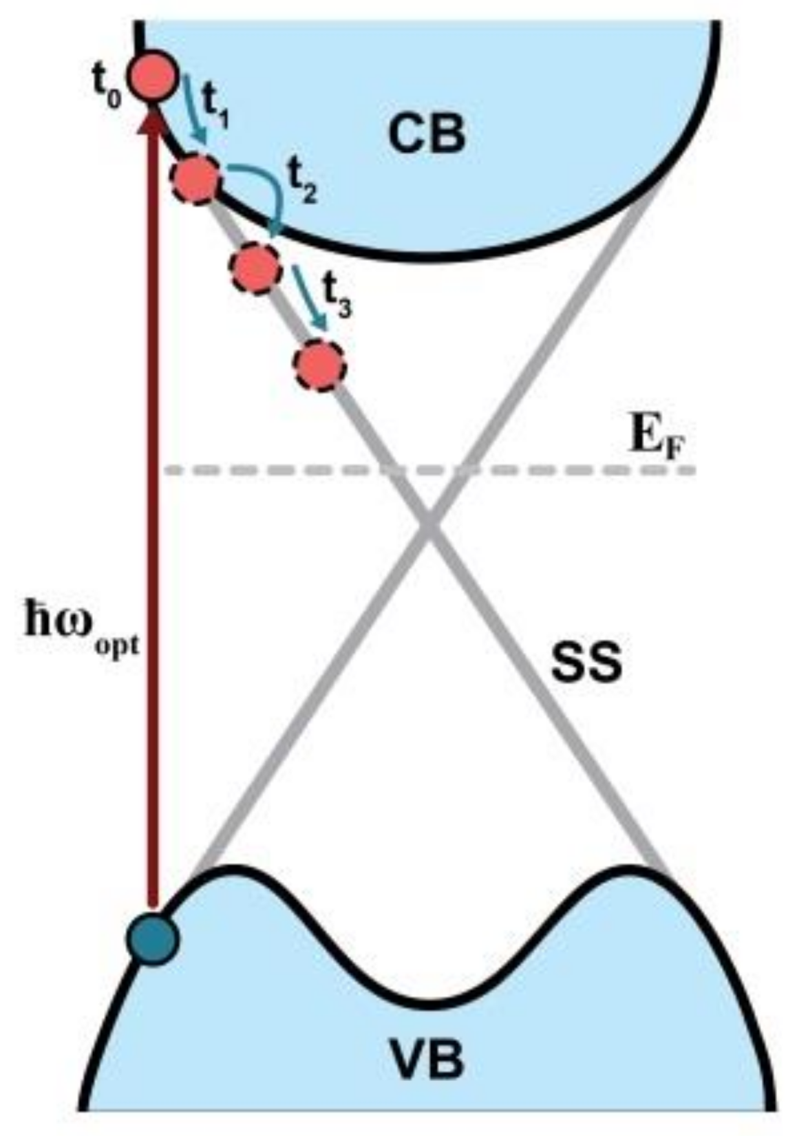
4. Discussion
5. Conclusions
Author Contributions
Funding
Institutional Review Board Statement
Informed Consent Statement
Acknowledgments
Conflicts of Interest
References
- Zhang, X.; Wang, J.; Zhang, S.-C. Topological insulators for high-performance terahertz to infrared applications. Phys. Rev. B 2010, 82, 245107. [Google Scholar] [CrossRef]
- Viti, L.; Coquillat, D.; Politano, A.; Kokh, K.A.; Aliev, Z.S.; Babanly, M.B.; Tereshchenko, O.E.; Knap, W.; Chulkov, E.V.; Vitiello, M.S. Plasma-Wave Terahertz Detection Mediated by Topological Insulators Surface States. Nano Lett. 2016, 16, 80–87. [Google Scholar] [CrossRef]
- West, D.; Zhang, S.B. Thin-film topological insulators for continuously tunable terahertz absorption. Appl. Phys. Lett. 2018, 112, 091601. [Google Scholar] [CrossRef]
- Li, C.H.; van ‘t Erve, O.M.J.; Yan, C.; Li, L.; Jonker, B.T. Electrical detection of current generated spin in topological insulator surface states: Role of interface resistance. Sci. Rep. 2019, 9, 6906. [Google Scholar] [CrossRef] [PubMed]
- Yan, P.; Lin, R.; Ruan, S.; Liu, A.; Chen, H.; Zheng, Y.; Chen, S.; Guo, C.; Hu, J. A practical topological insulator saturable absorber for mode-locked fiber laser. Sci. Rep. 2015, 5, 1–5. [Google Scholar] [CrossRef] [PubMed]
- He, M.; Sun, H.; He, Q.L. Topological insulator: Spintronics and quantum computations. Front. Phys. 2019, 14, 43401. [Google Scholar] [CrossRef]
- Ando, Y. Topological Insulator Materials. J. Phys. Soc. Jpn. 2013, 82, 102001. [Google Scholar] [CrossRef]
- Egorova, S.G.; Chernichkin, V.I.; Ryabova, L.I.; Skipetrov, E.P.; Yashina, L.; Danilov, S.N.; Ganichev, S.D.; Khokhlov, D.R. Detection of highly conductive surface electron states in topological crystalline insulators Pb1−xSnxSe using laser terahertz radiation. Sci. Rep. 2015, 5, 11540. [Google Scholar] [CrossRef] [PubMed]
- Luo, L.; Yang, X.; Liu, X.; Liu, Z.; Vaswani, C.; Cheng, D.; Mootz, M.; Zhao, X.; Yao, Y.; Wang, C.-Z.; et al. Ultrafast manipulation of topologically enhanced surface transport driven by mid-infrared and terahertz pulses in Bi2Se3. Nat. Commun. 2019, 10, 1–9. [Google Scholar] [CrossRef]
- Hamh, S.Y.; Park, S.-H.; Jerng, S.-K.; Jeon, J.H.; Chun, S.-H.; Lee, J.S. Helicity-dependent photocurrent in a Bi2Se3 thin film probed by terahertz emission spectroscopy. Phys. Rev. B 2016, 94, 161405. [Google Scholar] [CrossRef]
- Zhu, L.-G.; Kubera, B.; Mak, K.F.; Shan, J. Effect of Surface States on Terahertz Emission from the Bi2Se3 Surface. Sci. Rep. 2015, 5, 1–8. [Google Scholar] [CrossRef] [PubMed]
- Tu, C.-M.; Chen, Y.-C.; Huang, P.; Chuang, P.-Y.; Lin, M.-Y.; Cheng, C.-M.; Lin, J.-Y.; Juang, J.-Y.; Wu, K.-H.; Huang, J.-C.A.; et al. Helicity-dependent terahertz emission spectroscopy of topological insulator Sb2Te3 thin films. Phys. Rev. B 2017, 96, 195407. [Google Scholar] [CrossRef]
- Onishi, Y.; Ren, Z.; Novak, M.; Segawa, K.; Ando, Y.; Tanaka, K. Instantaneous Photon Drag Currents in Topological Insulators. arXiv 2014, arXiv:1403.2492. [Google Scholar]
- Plank, H.; Pernul, J.; Gebert, S.; Danilov, S.N.; König-Otto, J.; Winnerl, S.; Lanius, M.; Kampmeier, J.; Mussler, G.; Aguilera, I.; et al. Infrared/terahertz spectra of the photogalvanic effect in (Bi,Sb)Te based three-dimensional topological insulators. Phys. Rev. Mater. 2018, 2, 024202. [Google Scholar] [CrossRef]
- Fang, Z.; Wang, H.; Wu, X.; Shan, S.; Wang, C.; Zhao, H.; Xia, C.; Nie, T.; Miao, J.; Zhang, C.; et al. Non-linear terahertz emission in the three-dimensional topological insulator Bi2Te3 by terahertz emission spectroscopy. Appl. Phys. Lett. 2019, 115, 191102. [Google Scholar] [CrossRef]
- Ren, Z.; Taskin, A.A.; Sasaki, S.; Segawa, K.; Ando, Y. Optimizing Bi2−xSbxTe3−ySey solid solutions to approach the intrinsic topological insulator regime. Phys. Rev. B 2011, 84, 165311. [Google Scholar] [CrossRef]
- Castro-Camus, E.; Alfaro, M. Photoconductive devices for terahertz pulsed spectroscopy: A review. Photon. Res. 2016, 4, A36. [Google Scholar] [CrossRef]
- Burford, N.M.; El-Shenawee, M.O. Review of terahertz photoconductive antenna technology. Opt. Eng. 2017, 56, 010901. [Google Scholar] [CrossRef]
- Vieweg, N.; Rettich, F.; Deninger, A.; Roehle, H.; Dietz, R.; Göbel, T.; Schell, M. Terahertz-time domain spectrometer with 90 dB peak dynamic range. J. Infrared Millim. Terahertz Waves 2014, 35, 823–832. [Google Scholar] [CrossRef]
- Globisch, B.; Dietz, R.J.B.; Kohlhaas, R.B.; Göbel, T.; Schell, M.; Alcer, D.; Semtsiv, M.; Masselink, W.T. Iron doped InGaAs: Competitive THz emitters and detectors fabricated from the same photoconductor. J. Appl. Phys. 2017, 121, 053102. [Google Scholar] [CrossRef]
- Kohlhaas, R.B.; Breuer, S.; Nellen, S.; Liebermeister, L.; Schell, M.; Semtsiv, M.P.; Masselink, W.T.; Globisch, B. Photo-conductive terahertz detectors with 105 dB peak dynamic range made of rhodium doped InGaAs featured. Appl. Phys. Lett. 2019, 114, 221103. [Google Scholar] [CrossRef]
- Lepeshov, S.; Gorodetsky, A.; Krasnok, A.; Rafailov, E.; Belov, P. Enhancement of terahertz photoconductive antenna operation by optical nanoantennas. Laser Photonics Rev. 2017, 11, 1600199. [Google Scholar] [CrossRef]
- Yachmenev, A.E.; Lavrukhin, D.V.; Glinskiy, I.A.; Zenchenko, N.V.; Goncharov, Y.G.; Spektor, I.E.; Khabibullin, R.A.; Otsuji, T.; Ponomarev, D.S. Metallic and dielectric metasurfaces in photoconductive terahertz devices: A review. Opt. Eng. 2019, 59, 061608. [Google Scholar] [CrossRef]
- Kuznetsov, K.A.; Galiev, G.B.; Kitaeva, G.K.; Kornienko, V.V.; Klimov, E.A.; Klochkov, A.N.; Leontyev, A.A.; Pushkarev, S.S.; Malrsev, P.P. Photoconductive antennas based on epitaxial films In0.5Ga0.5As on GaAs (111)A and (100)A substrates with a metamorphic buffer. Laser Phys. Lett. 2018, 15, 076201. [Google Scholar] [CrossRef]
- Galiev, G.B.; Grekhov, M.M.; Kitaeva, G.K.; Klimov, E.A.; Klochkov, A.; Kolentsova, O.S.; Kornienko, V.; Kuznetsov, K.A.; Maltsev, P.; Pushkarev, S. Terahertz-radiation generation in low-temperature InGaAs epitaxial films on (100) and (411) InP substrates. Semiconductors 2017, 51, 310–317. [Google Scholar] [CrossRef]
- Zhang, Q.-L.; Si, L.-M.; Huang, Y.; Lv, X.; Zhu, W. Low-index-metamaterial for gain enhancement of planar terahertz antenna. AIP Adv. 2014, 4, 037103. [Google Scholar] [CrossRef]
- Hussain, N.; Nguyen, T.K.; Han, H.; Park, I. Minimum Lens Size Supporting the Leaky-Wave Nature of Slit Dipole Antenna at Terahertz Frequency. Int. J. Antennas Propag. 2016, 2016, 1–8. [Google Scholar] [CrossRef]
- Hussain, N.; Park, I. Design of a wide-gain-bandwidth metasurface antenna at terahertz frequency. AIP Adv. 2017, 7, 055313. [Google Scholar] [CrossRef]
- Llombart, N.; Chattopadhyay, G.; Skalare, A.; Mehdi, I. Novel Terahertz Antenna Based on a Silicon Lens Fed by a Leaky Wave Enhanced Waveguide. IEEE Trans. Antennas Propag. 2011, 59, 2160–2168. [Google Scholar] [CrossRef]
- Li, X.; Yin, W.; Khamas, S. An Efficient Photomixer Based Slot Fed Terahertz Dielectric Resonator Antenna. Sensors 2021, 21, 876. [Google Scholar] [CrossRef]
- Singh, A.; Pashkin, A.; Winnerl, S.; Welsch, M.; Beckh, C.; Sulzer, P.; Leitenstorfer, A.; Helm, M.; Schneider, H. Up to 70 THz bandwidth from an implanted Ge photoconductive antenna excited by a femtosecond Er:fibre laser. Light. Sci. Appl. 2020, 9, 1–7. [Google Scholar] [CrossRef]
- Kuznetsov, K.A.; Kitaeva, G.K.; Kuznetsov, P.I.; Yakushcheva, G.G. Generation of terahertz radiation from the island films of topological insulator Bi2−xSbxTe3−ySey. AIP Adv. 2019, 9, 015310. [Google Scholar] [CrossRef]
- Kuznetsov, K.; Klochkov, A.; Leontyev, A.; Klimov, E.; Pushkarev, S.; Galiev, G.; Kitaeva, G. Improved InGaAs and InGaAs/InAlAs Photoconductive Antennas Based on (111)-Oriented Substrates. Electronics 2020, 9, 495. [Google Scholar] [CrossRef]
- Braun, L.; Mussler, G.; Hruban, A.; Konczykowski, M.; Schumann, T.; Wolf, M.; Münzenberg, M.; Perfetti, L.; Kampfrath, T. Ultrafast photocurrents at the surface of the three-dimensional topological insulator Bi2Se3. Nat. Commun. 2016, 7, 13259. [Google Scholar] [CrossRef]
- Park, S.H.; Hamh, S.Y.; Park, J.; Kim, J.S.; Lee, J.S. Possible flat band bending of the Bi1.5Sb0.5Te1.7Se1.3 crystal cleaved in an ambient air probed by terahertz emission spectroscopy. Sci. Rep. 2016, 6, 36343. [Google Scholar] [CrossRef]
- Kuznetsov, K.A.; Kuznetsov, P.I.; Frolov, A.D.; Kovalev, S.P.; Ilyakov, I.E.; Ezhov, A.A.; Kitaeva, G.K. Bulk and surface terahertz conductivity of Bi2−xSbxTe3−ySey topological insulators. Opt. Eng. 2021, 60, 082012. [Google Scholar] [CrossRef]
- Lorenc, M.; Onishi, Y.; Ren, Z.; Segawa, W.; Kaszub, W.; Ando, Y.; Tanaka, K. Ultrafast carrier relaxation through Auger recombination in the topological insulatorBi1.5Sb0.5Te1.7Se1.3. Phys. Rev. B 2015, 91, 085306. [Google Scholar] [CrossRef]
- Sobota, J.A.; Yang, S.; Analytis, J.G.; Chen, Y.L.; Fisher, I.R.; Kirchmann, P.S.; Shen, Z.-X. Ultrafast Optical Excitation of a Persistent Surface-State Population in the Topological Insulator Bi2Se3. Phys. Rev. Lett. 2012, 108, 117403. [Google Scholar] [CrossRef]
- Kovalev, S.; Tielrooij, K.-J.; Deinert, J.-C.; Ilyakov, I.; Awari, N.; Chen, M.; Ponomaryov, A.; Bawatna, M.; de Oliveira, T.V.A.G.; Eng, L.M.; et al. Terahertz signatures of ultrafast Dirac fermion relaxation at the surface of topological insulators at room temperature. arXiv 2006, arXiv:2006.03948. [Google Scholar]
- Plank, H.; Ganichev, S.D. A review on terahertz photogalvanic spectroscopy of Bi2Te3- and Sb2Te3-based three dimensional topological insulators. Solid State Electron. 2018, 147, 44–50. [Google Scholar] [CrossRef]
- Plank, H.; Golub, L.E.; Bauer, S.; Bel’kov, V.V.; Herrmann, T.; Olbrich, P.; Eschbach, M.; Plucinski, L.; Schneider, C.M.; Kampmeier, J.; et al. Photon drag effect in(Bi1−xSbx)2Te3 three-dimensional topological insulators. Phys. Rev. B 2016, 93, 125434. [Google Scholar] [CrossRef]
- Il’inskii, Y.A.; Keldysh, L.V. General Theory of Interaction of Electromagnetic Fields with Matter. In Electromagnetic Response of Material Media; Springer: Boston, MA, USA, 1994. [Google Scholar]


Publisher’s Note: MDPI stays neutral with regard to jurisdictional claims in published maps and institutional affiliations. |
© 2021 by the authors. Licensee MDPI, Basel, Switzerland. This article is an open access article distributed under the terms and conditions of the Creative Commons Attribution (CC BY) license (https://creativecommons.org/licenses/by/4.0/).
Share and Cite
Kuznetsov, K.A.; Safronenkov, D.A.; Kuznetsov, P.I.; Kitaeva, G.K. Terahertz Photoconductive Antenna Based on a Topological Insulator Nanofilm. Appl. Sci. 2021, 11, 5580. https://doi.org/10.3390/app11125580
Kuznetsov KA, Safronenkov DA, Kuznetsov PI, Kitaeva GK. Terahertz Photoconductive Antenna Based on a Topological Insulator Nanofilm. Applied Sciences. 2021; 11(12):5580. https://doi.org/10.3390/app11125580
Chicago/Turabian StyleKuznetsov, Kirill A., Daniil A. Safronenkov, Petr I. Kuznetsov, and Galiya Kh. Kitaeva. 2021. "Terahertz Photoconductive Antenna Based on a Topological Insulator Nanofilm" Applied Sciences 11, no. 12: 5580. https://doi.org/10.3390/app11125580
APA StyleKuznetsov, K. A., Safronenkov, D. A., Kuznetsov, P. I., & Kitaeva, G. K. (2021). Terahertz Photoconductive Antenna Based on a Topological Insulator Nanofilm. Applied Sciences, 11(12), 5580. https://doi.org/10.3390/app11125580