
Rapid 3D-Imaging of Semiconductor Chips Using THz Time-of-Flight Technique

 and
and 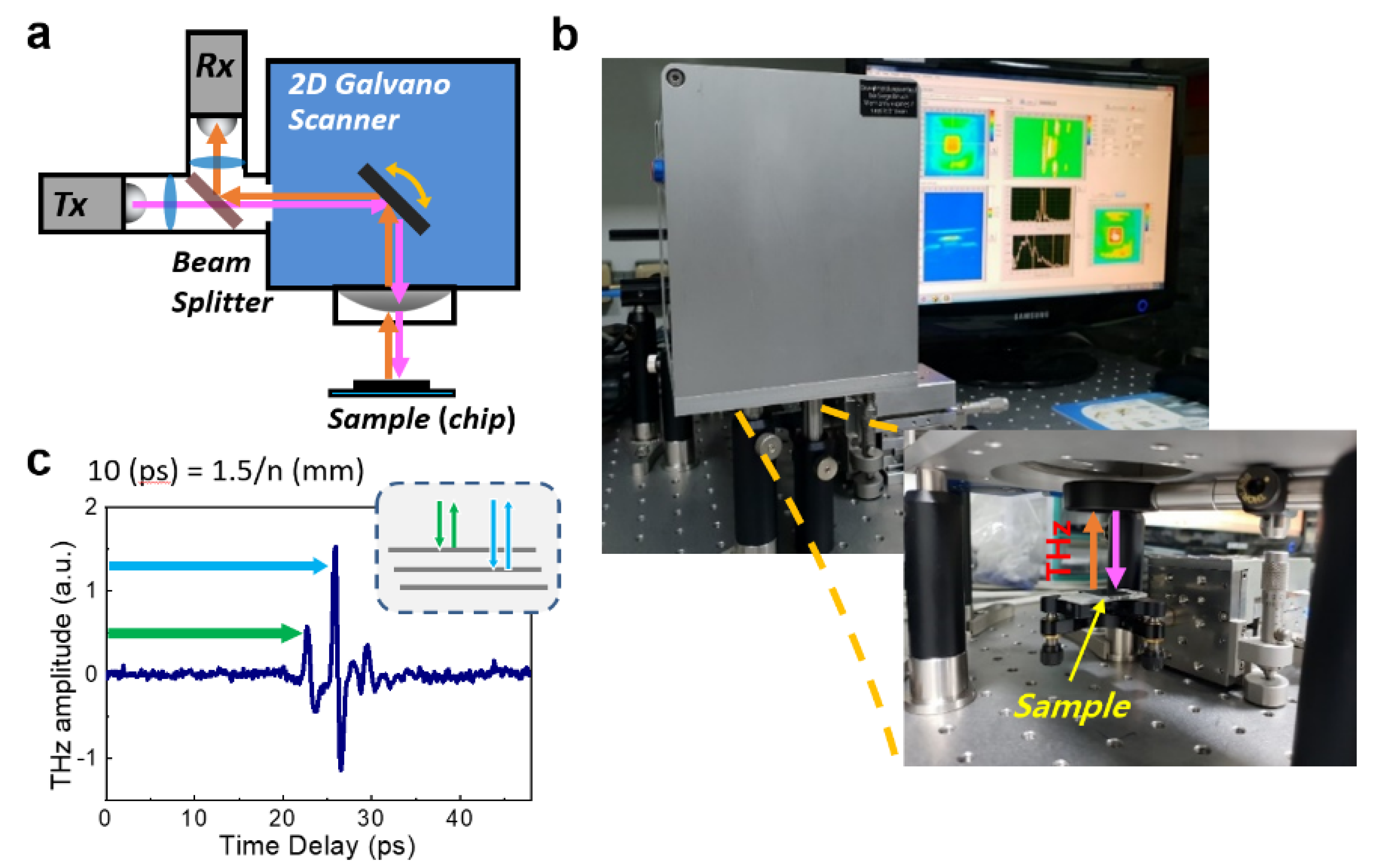
Abstract
:1. Introduction
2. Experimental Setup
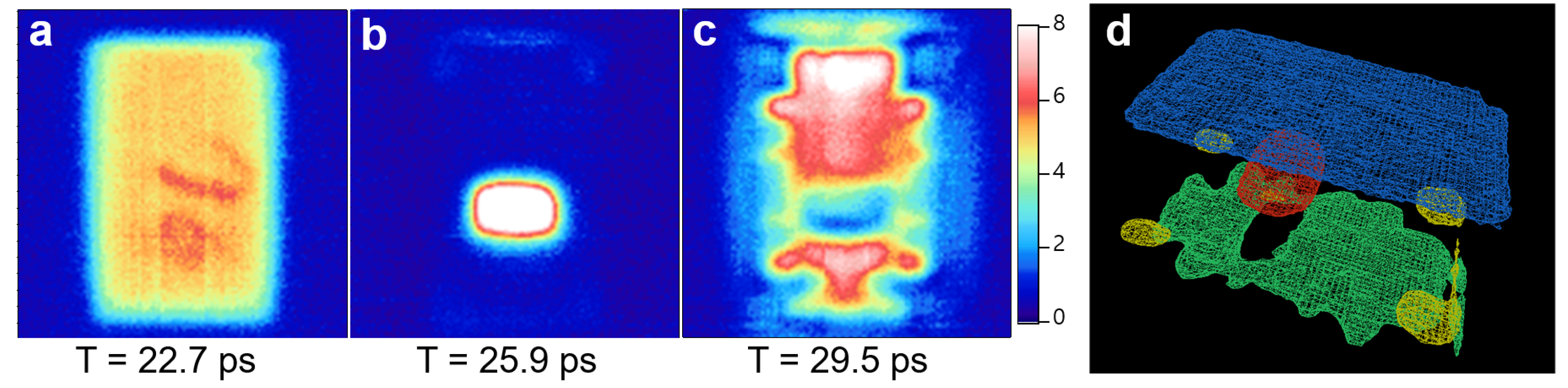
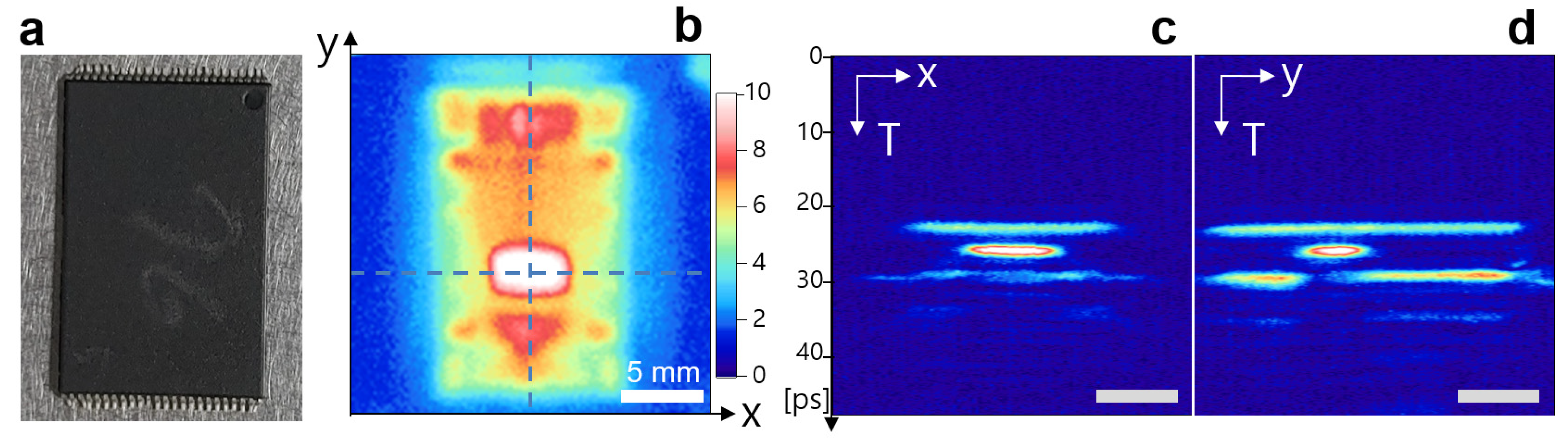
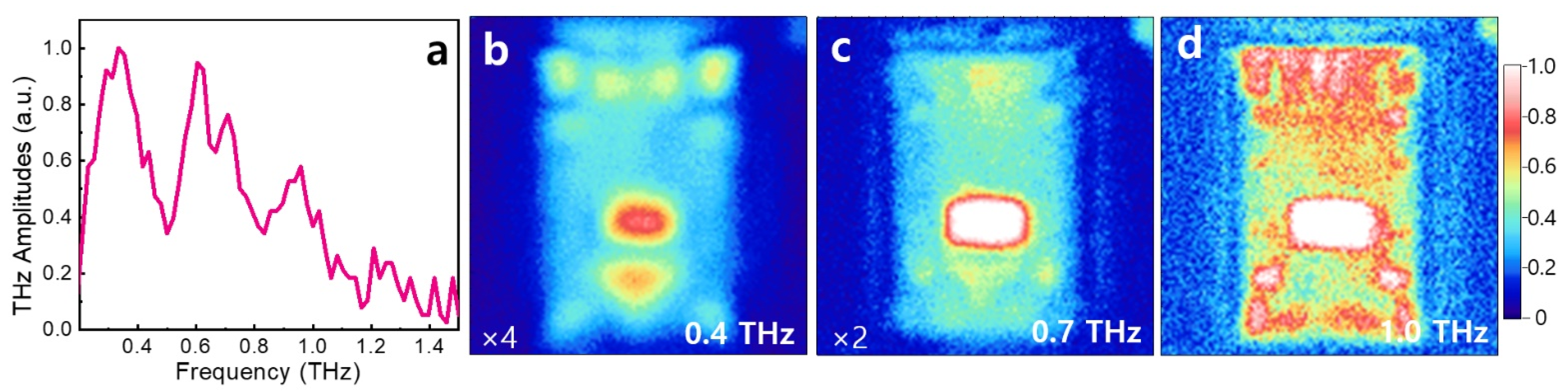
3. Results and Discussion
4. Conclusions
Author Contributions
Funding
Institutional Review Board Statement
Informed Consent Statement
Data Availability Statement
Conflicts of Interest
References
- Ogawa, Y.; Hayashi, S.I.; Oikawa, M.; Otani, C.; Kawase, K. Interference terahertz label-free imaging for protein detection on a membrane. Opt. Express 2008, 16, 22083–22089. [Google Scholar] [CrossRef] [PubMed]
- Tomaino, J.L.; Jameson, A.D.; Paul, M.J.; Kevek, J.W.; van der Zande, A.M.; Barton, R.A.; Choi, H.; McEuen, P.L.; Minot, E.D.; Lee, Y.-S. High-Contrast Imaging of Graphene via Time-Domain Terahertz Spectroscopy. J. Infrared Millim. Terahertz Waves 2012, 33, 839–845. [Google Scholar] [CrossRef] [Green Version]
- Park, S.-H.; Jang, J.-W.; Kim, H.-S. Non-destructive evaluation of the hidden voids in integrated circuit packages using terahertz time-domain spectroscopy. J. Micromech. Microeng. 2015, 25, 095007. [Google Scholar] [CrossRef]
- Zhong, S.; Shen, Y.-C.; Ho, L.; May, R.K.; Zeitler, J.A.; Evans, M.; Taday, P.F.; Pepper, M.; Rades, T.; Gordon, K.C.; et al. Non-destructive quantification of pharmaceutical tablet coatings using terahertz pulsed imaging and optical coherence tomography. Opt. Lasers Eng. 2011, 49, 361–365. [Google Scholar] [CrossRef] [Green Version]
- Park, S.J.; Hong, J.T.; Choi, S.J.; Kim, H.S.; Park, W.K.; Han, S.T.; Park, J.Y.; Lee, S.; Kim, D.S.; Ahn, Y.H. Detection of microorganisms using terahertz metamaterials. Sci. Rep. 2014, 4, 4988. [Google Scholar] [CrossRef] [PubMed]
- Kim, H.S.; Ha, N.Y.; Park, J.-Y.; Lee, S.; Kim, D.-S.; Ahn, Y.H. Phonon-Polaritons in Lead Halide Perovskite Film Hybridized with THz Metamaterials. Nano Lett. 2020, 20, 6690–6696. [Google Scholar] [CrossRef] [PubMed]
- Ahi, K.; Shahbazmohamadi, S.; Asadizanjani, N. Quality control and authentication of packaged integrated circuits using enhanced-spatial-resolution terahertz time-domain spectroscopy and imaging. Opt. Lasers Eng. 2018, 104, 274–284. [Google Scholar] [CrossRef]
- Federici, J.F.; Schulkin, B.; Huang, F.; Gary, D.; Barat, R.; Oliveira, F.; Zimdars, D. THz imaging and sensing for security applications—explosives, weapons and drugs. Semicond. Sci. Technol. 2005, 20, S266–S280. [Google Scholar] [CrossRef]
- Shen, Y.C.; Lo, T.; Taday, P.F.; Cole, B.E.; Tribe, W.R.; Kemp, M.C. Detection and identification of explosives using terahertz pulsed spectroscopic imaging. Appl. Phys. Lett. 2005, 86, 241116. [Google Scholar] [CrossRef] [Green Version]
- Fan, S.; Li, T.; Zhou, J.; Liu, X.; Liu, X.; Qi, H.; Mu, Z. Terahertz non-destructive imaging of cracks and cracking in structures of cement-based materials. Aip Adv. 2017, 7, 115202. [Google Scholar] [CrossRef] [Green Version]
- Hua, Z.; Jingzhou, X.; Xu, X.; Tao, Y.; Reightler, R.; Madaras, E.; Xi-Cheng, Z. Nondestructive defect identification with terahertz time-of-flight tomography. IEEE Sens. J. 2005, 5, 203–208. [Google Scholar] [CrossRef]
- Jin, K.H.; Kim, Y.-G.; Cho, S.H.; Ye, J.C.; Yee, D.-S. High-speed terahertz reflection three-dimensional imaging for nondestructive evaluation. Opt. Express 2012, 20, 25432–25440. [Google Scholar] [CrossRef]
- Karpowicz, N.; Redo, A.; Hua, Z.; Xia, L.; Jingzhou, X.; Zhang, X.C. Continuous-Wave Terahertz Imaging for Non-Destructive Testing Applications. In Proceedings of the 2005 Joint 30th International Conference on Infrared and Millimeter Waves and 13th International Conference on Terahertz Electronics, Williamsburg, VA, USA, 19–23 September 2005; Volume 321, pp. 329–330. [Google Scholar]
- Kawase, K.; Ogawa, Y.; Watanabe, Y.; Inoue, H. Non-destructive terahertz imaging of illicit drugs using spectral fingerprints. Opt. Express 2003, 11, 2549–2554. [Google Scholar] [CrossRef] [Green Version]
- Kawase, K.; Shibuya, T.; Hayashi, S.i.; Suizu, K. THz imaging techniques for nondestructive inspections. Comptes Rendus Phys. 2010, 11, 510–518. [Google Scholar] [CrossRef]
- Schirmer, M.; Fujio, M.; Minami, M.; Miura, J.; Araki, T.; Yasui, T. Biomedical applications of a real-time terahertz color scanner. Biomed. Opt. Express 2010, 1, 354–366. [Google Scholar] [CrossRef] [PubMed] [Green Version]
- Zhang, J.-Y.; Ren, J.-J.; Li, L.-J.; Gu, J.; Zhang, D.-D. THz imaging technique for nondestructive analysis of debonding defects in ceramic matrix composites based on multiple echoes and feature fusion. Opt. Express 2020, 28, 19901–19915. [Google Scholar] [CrossRef] [PubMed]
- Lien Nguyen, K.; Johns, M.L.; Gladden, L.F.; Worrall, C.H.; Alexander, P.; Beere, H.E.; Pepper, M.; Ritchie, D.A.; Alton, J.; Barbieri, S.; et al. Three-dimensional imaging with a terahertz quantum cascade laser. Opt. Express 2006, 14, 2123–2129. [Google Scholar] [CrossRef]
- Karpowicz, N.; Zhong, H.; Xu, J.; Lin, K.-I.; Hwang, J.-S.; Zhang, X.C. Comparison between pulsed terahertz time-domain imaging and continuous wave terahertz imaging. Semicond. Sci. Technol. 2005, 20, S293–S299. [Google Scholar] [CrossRef]
- Ok, G.; Park, K.; Kim, H.J.; Chun, H.S.; Choi, S.-W. High-speed terahertz imaging toward food quality inspection. Appl. Opt. 2014, 53, 1406–1412. [Google Scholar] [CrossRef]
- Karpowicz, N.; Zhong, H.; Zhang, C.; Lin, K.-I.; Hwang, J.-S.; Xu, J.; Zhang, X.-C. Compact continuous-wave subterahertz system for inspection applications. Appl. Phys. Lett. 2005, 86, 054105. [Google Scholar] [CrossRef] [Green Version]
- Lee, I.-S.; Lee, J.W. Nondestructive Internal Defect Detection Using a CW–THz Imaging System in XLPE for Power Cable Insulation. Appl. Sci. 2020, 10, 2055. [Google Scholar] [CrossRef] [Green Version]
- Kim, J.-Y.; Song, H.-J.; Yaita, M.; Hirata, A.; Ajito, K. CW-THz vector spectroscopy and imaging system based on 1.55-µm fiber-optics. Opt. Express 2014, 22, 1735–1741. [Google Scholar] [CrossRef] [PubMed]
- Moon, K.; Lee, I.-M.; Lee, E.S.; Park, K.H. Photonics-Based Multi-Spectral THz Imaging Using a Dual-Mode Laser and a Telecentric f-θ Lens. In Proceedings of the Conference on Lasers and Electro-Optics, San Jose, CA, USA, 5 May 2019; p. STu3F.7. [Google Scholar]
- Nagatsuma, T.; Nishii, H.; Ikeo, T. Terahertz imaging based on optical coherence tomography [Invited]. Photon. Res. 2014, 2, B64–B69. [Google Scholar] [CrossRef]
- Cristofani, E.; Friederich, F.; Wohnsiedler, S.; Matheis, C.; Jonuscheit, J.; Vandewal, M.; Beigang, R. Nondestructive testing potential evaluation of a terahertz frequency-modulated continuous-wave imager for composite materials inspection. Opt. Eng. 2014, 53, 031211. [Google Scholar] [CrossRef]
- Yahng, J.S.; Park, C.-S.; Don Lee, H.; Kim, C.-S.; Yee, D.-S. High-speed frequency-domain terahertz coherence tomography. Opt. Express 2016, 24, 1053–1061. [Google Scholar] [CrossRef]
- Bartels, A.; Cerna, R.; Kistner, C.; Thoma, A.; Hudert, F.; Janke, C.; Dekorsy, T. Ultrafast time-domain spectroscopy based on high-speed asynchronous optical sampling. Rev. Sci. Instrum. 2007, 78, 035107. [Google Scholar] [CrossRef] [Green Version]
- Wilk, R.; Hochrein, T.; Koch, M.; Mei, M.; Holzwarth, R. OSCAT: Novel Technique for Time-Resolved Experiments without Moveable Optical Delay Lines. J. Infrared Millim. Terahertz Waves 2011, 32, 596–602. [Google Scholar] [CrossRef]
- Kong, D.-Y.; Wu, X.-J.; Wang, B.; Gao, Y.; Dai, J.; Wang, L.; Ruan, C.-J.; Miao, J.-G. High resolution continuous wave terahertz spectroscopy on solid-state samples with coherent detection. Opt. Express 2018, 26, 17964–17976. [Google Scholar] [CrossRef]
- Lei, W.-S.; Kumar, A. Delamination and Reliability Issues in Packaged Devices. In Adhesion in Microelectronics; John Wiley & Sons: Hoboken, NJ, USA, 2014; pp. 267–312. [Google Scholar]
- Piesiewicz, R.; Jansen, C.; Wietzke, S.; Mittleman, D.; Koch, M.; Kürner, T. Properties of Building and Plastic Materials in the THz Range. Int. J. Infrared Millim. Waves 2007, 28, 363–371. [Google Scholar] [CrossRef]
- Stübling, E.; Gomell, L.; Sommer, S.; Winkel, A.; Kahlmeyer, M.; Böhm, S.; Koch, M. THz Properties of Adhesives. J. Infrared Millim. Terahertz Waves 2018, 39, 586–593. [Google Scholar] [CrossRef]


Publisher’s Note: MDPI stays neutral with regard to jurisdictional claims in published maps and institutional affiliations. |
© 2021 by the authors. Licensee MDPI, Basel, Switzerland. This article is an open access article distributed under the terms and conditions of the Creative Commons Attribution (CC BY) license (https://creativecommons.org/licenses/by/4.0/).
Share and Cite
Yim, J.H.; Kim, S.-y.; Kim, Y.; Cho, S.; Kim, J.; Ahn, Y.H. Rapid 3D-Imaging of Semiconductor Chips Using THz Time-of-Flight Technique. Appl. Sci. 2021, 11, 4770. https://doi.org/10.3390/app11114770
Yim JH, Kim S-y, Kim Y, Cho S, Kim J, Ahn YH. Rapid 3D-Imaging of Semiconductor Chips Using THz Time-of-Flight Technique. Applied Sciences. 2021; 11(11):4770. https://doi.org/10.3390/app11114770
Chicago/Turabian StyleYim, Jong Hyuk, Su-yeon Kim, Yiseob Kim, Suyoung Cho, Jangsun Kim, and Yeong Hwan Ahn. 2021. "Rapid 3D-Imaging of Semiconductor Chips Using THz Time-of-Flight Technique" Applied Sciences 11, no. 11: 4770. https://doi.org/10.3390/app11114770
APA StyleYim, J. H., Kim, S.-y., Kim, Y., Cho, S., Kim, J., & Ahn, Y. H. (2021). Rapid 3D-Imaging of Semiconductor Chips Using THz Time-of-Flight Technique. Applied Sciences, 11(11), 4770. https://doi.org/10.3390/app11114770