Article

Numerical Study of Multilayer Planar Film Structures for Ideal Absorption in the Entire Solar Spectrum

1
Navigation Institute, Jimei University, Xiamen 361021, China
2
School of Information Engineering, Jimei University, Xiamen 361021, China
3
Ocean College, Zhejiang University, Zhoushan 316000, China
4
Department of Chemical and Materials Engineering, National University of Kaohsiung, Kaohsiung 0000800, Taiwan
*
Authors to whom correspondence should be addressed.
Appl. Sci. 2020, 10(9), 3276; https://doi.org/10.3390/app10093276
Submission received: 7 April 2020 / Revised: 25 April 2020 / Accepted: 27 April 2020 / Published: 8 May 2020

Abstract

:

Featured Application

Solar energy is the most important clean energy source on the earth, and many research studies have been conducted to investigate solar-energy collection. This article numerically proposes a new ultra-broadband solar absorber with structures of multilayer planar films for solar thermal energy conversion. The high absorption rate of designed multilayer planar films mainly results from the multiple asymmetric highly lossy Fabry–Perot resonators by the laminated structures of the intrinsic SiO2 dielectric absorption in the wide wavelength range by the refractory of different non-noble metals. The proposed absorber of multilayer planar films could have broad application prospects in hot-electron devices and solar-energy harvesting.

Abstract

Here, we have theoretically proposed an ideal structure of selective solar absorber with multilayer planar films, which can absorb the incident light throughout the entire solar spectrum (300–2500 nm) and over a wide angular range, whatever the polarization angle of 0°~90°. The efficiency of the proposed absorber is proven by the Finite-Difference Time Domain (FDTD) simulation. The average absorption rate over the solar spectrum is up to 96.6%. The planar design is extremely easy to fabricate and modify, and this structure does not require lithographic processes to finish the absorbers. Improvements of the solar absorber on the basis of planar multilayer-film structures is attributed to multiple asymmetric highly lossy Fabry–Perot resonators. Because of having many virtues, such as using different refractory and non-noble metals, having angle and polarization independence, and having ideal absorption for entire solar spectrum, our proposed absorbers are promising candidates for practical industrial production of the solar-energy harvesting.

1. Introduction

In the past decade, the increasing cost of fossil fuels and the global warming problem have increased the urgency of the need to develop renewable green energy (such as solar, wind, tidal, etc.) [1]. Because of having the properties of security, universality, and other advantages, the transformation solar energy to useful energies has been a field of intensive researches in recent years. Functionally, there are two major conversion mechanisms of solar energy: photovoltaic and solar-thermal applications [2,3]. In solar-thermal conversion devices, many researches have aimed to convert the incident solar light to heat for further application. The key component is using a solar absorber, which can provide ideal absorption of sunlight over the entire solar spectrum and convert solar energy to other energy that we can utilize [4]. Many solar-thermal applications can be directly applied in many industrial processes, such as water purification, desalination, distillation, and so on [5,6]. Besides, for thermophotovoltaic (TPV) devices, the thermal energy can also be converted to electricity energy [7]. It effectively traps the incident light in the nanospaces and dissipates it by the ohmic losses of the metal that can give rise to the high absorption rate of the incident light. For that plasmonic metamaterial absorbers have attracted considerable attention for the harvesting of solar energy [8]. Chen et al. proposed a dual functional asymmetric plasmonic absorber for solar water purification and pollution detection [5]. Tan et al. reported a plasmonic absorbers which can enable a strong absorption rate (72–91%), over 400–900 nm, and a significantly (20-fold) enhanced photocurrent as compared to the bare TiO2 film for enhanced photocurrent of visible-light photocatalysis [7]. Lin et al. proposed a 90-nm-thick graphene sheet absorber, which can be heated to 160 °C in natural sunlight [9]. When light interacts with nanostructured absorbers, the energy is confined in a nanospace, and this confinement can lead to heat generation. Thus, many various nanostructures based on metals have been proposed for the absorption enhancement. For instance, Cong et al. investigated a broadband visible-light absorber via hybridization of propagating surface plasmon (PSP), and the average absorption rate of the designed absorber could reach up to nearly 90% in the visible range of 400~750 nm [10]. Aydin et al. demonstrated experimentally plasmonic super absorbers that are capable of absorbing light from 400 nm to 700 nm, with a measured average absorption rate of 71% [11]. Tang et al. theoretically proposed absorbers based on concentric multi-split-ring arrays with which the average absorption rate reaches 97.2% over the wavelength range from 585 to 800 nm [12]. Li et al. experimentally demonstrated an omnidirectional broadband-light absorber, using large-area ultrathin lossy metallic film coatings [13].
However, it is obvious that simply designing structures is not sufficient for building a solar device, because the narrowband plasmonic resonance of metal nanoarrays only allows the utilization of a small fraction of light in the solar spectrum (300–2500 nm). It is therefore highly desirable to design solar absorbers with a high solar absorption rate, to significantly enhance the conversion efficiency from sunlight to heat. In order to enhance absorption rate of sunlight, researchers have investigated many different kinds of complex models. Wan et al. proposed a patterned gold (Au)-carbon (C)-gold (Au) structure to realize a metasurface absorber with a selective high absorption, ranging from 400 to 1200 nm [14]. Wu et al. theoretically investigated a selective solar absorber consisting of tungsten nanoparticle arrays embedded in a silica layer deposited on alternating tungsten/silica layers with an extremely high absorption efficiency, above 99%, within the range of 435–1520 nm [15]. Lin et al. proposed a 90-nm-thick graphene sheet absorber with approximately 85% absorption of unpolarized visible and near-infrared light covering almost the entire solar spectrum (300–2500 nm) [9]. However, some of reported solar absorbers are typically fabricated by using noble metals (e.g., gold and silver), because they have excellent surface plasmon polarization [16,17], but they have the problem of high cost, which limits the practical applications in the solar absorbers. Moreover, graphene sheets (2-nm-thick carbon layers), femtosecond laser, and other lithographic processes limited the wide application of this absorber and increased its manufacturing cost. Therefore, designing a solar absorber with the advantages of ideal broadband absorption, and fabrication simplicity still represents great challenges.
Since the solar-thermal applications need to work at extremely high temperatures, the use of refractory metals is necessary. For example, bulk Chromium (Cr) has a high melting temperature of 2180 K, which is relative to the blackbody radiation at a peak position of 1.33 μ m . However, the melting temperature of bulk gold (Au) is about 1337 K relative to a peak position of 2.17 μ m for the blackbody radiation. The spectral density B λ ( λ , T ) of thermal radiation from a black body absorber can be defined by Planck’s law:
B λ ( λ , T ) = 2 h c 2 λ 5 1 e h c λ k T 1
where λ is the wavelength, T is the absolute temperature of the black body absorber, h is Planck constant, and k is the Boltzmann constant [18]. Maximum radiation for absolute temperatures, T = 1337 and 2180 K, will occur at 1.33 and 2.17 μm, respectively.
Although the melting temperatures for metals at the nanoscale will be below their bulk values due to small size effects, refractory metals still have higher melting temperatures than those of noble metals [13]. For example, the melting temperatures of Titanium (Ti), iron (Fe), and Cr are 1941, 1811, and 2180 K, while the melting temperatures of Au and Argentum (Ag) are 1337 and 1234 K, respectively, as shown in Table 1. Besides, Wu et al. proved that Fe arrays had the advantageous impedance matching effect between the structure of multilayer films and the free space could be achieved over an ultra-broad band of optical frequency (from visible to near-infrared region), which could play an extremely important role to construct an ideal absorption device in solar bandwidth [19]. Moreover, Li et al. showed that Cr has optical lossy properties and less optical dispersive properties, and SiO2 has a high transparency broadband window with non-dispersive optical characteristics in the range of visible light [13].
Therefore, the selection of appropriate materials for the design of a high-efficiency absorber is very important. Here, we propose a high-efficiency absorber with simple a multilayer structure, which could enable omnidirectional, polarization-independent, and broadband absorption across the entire solar bandwidth. The efficiency of proposed absorber could be proven by the Finite-Difference Time Domain (FDTD) simulation. To the best of our knowledge, numerical analysis describe that the designed absorber has a high average absorption rate of 96.6% in the range of 300–2500 nm, which is higher than all previously reported solar absorbers listed in Table 2 [9,13,15,19]. The high absorption is not only completely independent of polarization direction but also exhibits angle-independent absorption behavior for oblique incidences up to ±60 degree. Such a designed absorber is simpler as compared with those of patterning structures. This investigated structure signifies that the solar absorber can be designed to have the advantages of non-noble-metal manufacturing convenience because of its extremely simple structure and higher performance for practical industrial production. For that, the designed absorber can be used as the devices to enhance the use of clean energy because it has high harvesting efficiency for solar energy [20,21,22].

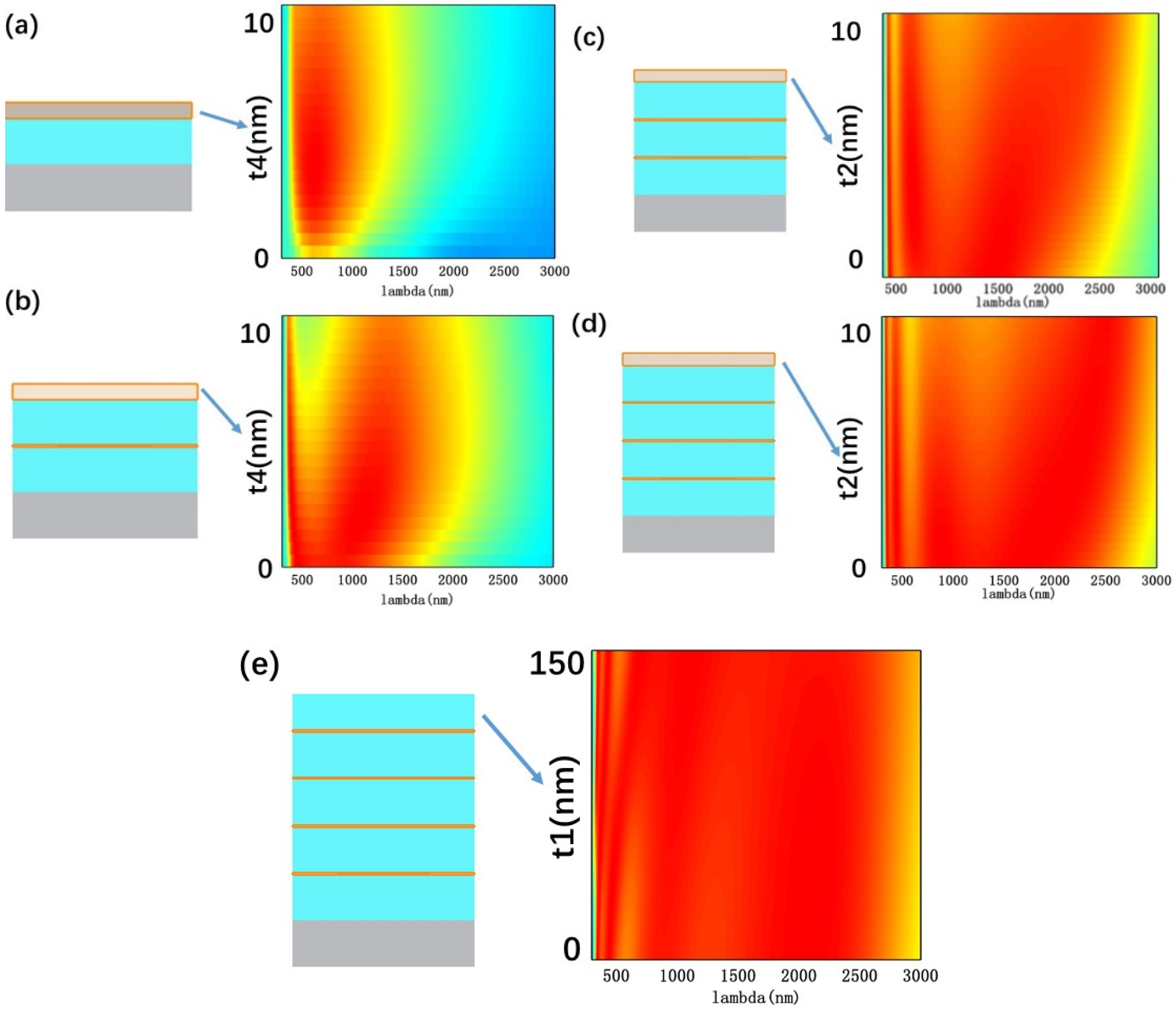
2. Materials, Structure, and Methods

A schematic diagram of planar multilayer films’ designed structure is displayed in Figure 1, which has some important novelties in this designed absorber. The first novelty is that the top MgF2 layer is not only designed as an anti-corrosion layer to prevent iron from being oxidized, but it is also designed as an anti-reflective film. The second novelty is that the bottom Fe layer is designed as a backside reflector. The third novelty is that the addition of SiO2 can be used as a separator of different metals. The related geometric parameters of the designed absorber are labeled in Figure 1. MgF2 and SiO2 can be considered to be the lossless dielectric materials; their refractive indexes are 1.38 and 1.45, respectively. The electromagnetic parameters of the Fe, Cr, and Ti are taken from the CRC Handbook of Chemistry and Physics [23].
In order to design a solar absorber with the optimal absorption rate, our proposed device’s structure is numerically demonstrated and optimized by using the FDTD simulation [24]. The FDTD method, as well as Maxwell’s Solver, is one of the most frequently used numerical techniques for computing optical properties, and it can construct a gold-standard for modeling nanophotonic devices, processes, and materials. Specifically, we used a commercially available FDTD simulation software package of Lumerical Inc. The reliability and accuracy of the numerical results were ensured by many reports [11,12,13,25,26,27,28]. The period boundary conditions are used in the x-axis and y-axis directions, and an ideally matched layer boundary condition is set in the z-axis direction. A plane wave with TM polarization with the electric field and magnetic field respectively polarized in the directions of x-axis and y-axis is normally incident onto the proposed absorber. The absorption rate (A) can be defined as follows: A = 1 R T , where the R and T indicate reflection and transmission rates, respectively. Because the thickness of the backside Fe layer is smaller than the skin depth in the infrared light spectrum, the T is set as zero. For that, the absorption rate is reduced to: A = 1 − R.

3. Results and Discussions

Since our proposed absorber has a structure composed of multilayer planar films, we analyzed the structure with Fe-SiO2-Fe (structure A), firstly so as to further analyze the ideal broadband absorption. The simple Fe-SiO2-Fe multilayer films can be recognized as a structure of asymmetric F–P nano-cavity, which consists of a sandwich structure. The core is lossless dielectric layer, the top layer is a lossy metal layer, and the backside layer is a reflector, as the schematic diagram in Figure 2a shows. As the results in Figure 2a,b show, since an ordinary F–P nano-cavity absorber is usually characterized by high wavelength selectivity in absorption spectra, the absorption of Structure A maintains a high level in the wavelength of visible spectrum, but declines in the wavelength of infrared spectrum. In order to obtain the better insights of the physical mechanism for the high absorption rate in the visible spectrum, we calculated the spatial distribution of magnetic field (Hy) and absorbed power distributions over the cross-section at the absorption peaks λ = 620 nm, as labeled in Figure 2c,d, separately.
The absorbed-power distribution can be defined as P a b s = · s = 1 2 ω ε | E | 2 for nonmagnetic material, where ε is the imaginary part of the permittivity, ω is the angular frequency, and | E | is the total electric field distribution [29]. The distribution of magnetic field (Hy) is shown to be highly limited by the boundary opaque metals (Fe layers) and trapped in the dielectric core (SiO2 layer), as shown in Figure 2c shows. The resonance is considered to be the PSP resonance between the interface of Fe and SiO2 films. According to the calculated absorbed-power distribution, the reason to reach the high absorption rate is the loss of top thin Fe layer, as well as that of backside Fe reflector. However, the main reason to cause the absorbed-power distribution is due to the top Fe layer, accounting for much larger than the dissipation inside the backside Fe layer. Thus, the distribution of magnetic field and absorbed-power distribution are illustrated in Figure 2c,d, respectively, which indicate a combination of the PSP and F–P resonances.
One can see from Figure 2b that, although Structure A can form an absorber with a high absorption rate, the absorption bandwidth is narrow and the absorption efficiency is low, and these things will limit its practical application. In order to overcome the above shortcomings, a simple method can be investigated to improve these problems, using vertical superposition of the multilayer plane films, to enable the enhancement of spectral absorption. As shown in Figure 3a, the absorption rate of Cr-SiO2-Fe-SiO2-Fe (Structure B) is higher than that of Structure A; however, it still has a problem of having an absorption bandwidth that is too narrow and a discontinuous absorption rate. Furthermore, the absorption rate of Ti-Cr-SiO2-Fe-SiO2-Fe (Structure C) is shown in Figure 3b. One can see that the high absorption rate does not cover the entire solar spectrum, especially in the range of 2000–2500 nm. Nevertheless, we can find that the absorption bandwidth and efficiency is limited in the above-proposed solar absorbers. As a matter of fact, the absorption bandwidth and efficiency play a key role in many actual applications, e.g., thermal emitters, solar energy utilizations, photodetector applications, and so on. In order to achieve an ideal absorption in the entire solar spectrum shown in Figure 3d, the structure of the designed multilayer absorber is determined to be MgF2 (anti-reflection layer)-Ti-SiO2-Cr-SiO2-Fe-SiO2-Fe (Structure D), as Figure 3c shows, which can obtain an ideal absorption throughout the entire solar spectrum (300–2500 nm).
Incident light on a metal surface will produce a reflection. Therefore, for reducing the reflection of incident light of an absorber, a multilayer design is usually carried out. As we all know, the higher the refractive index, the stronger the transmittance of the incident light. The refractive index of MgF2 is 1.38, which is much lower than that of ordinary dielectric medium. Therefore, we choose MgF2 film as the antireflection layer. The average absorption is defined as follows:
A = λ 1 λ 2 A ( λ ) d λ / ( λ 1 λ 2 )
where λ 1 and λ 2   respectively are 2500 and 300 nm. From our numerical simulation results, the average absorption will reach 96.6% over the wavelength region of 300~2500 nm. It can be seen clearly in Figure 3c that the high absorption rate is really obtained in the wavelength range of 300~2500 nm. The gray curve in Figure 3d is the air mass 1.5 solar irradiance spectrum, i.e., the entire solar spectrum (300–2500 nm). Figure 3d can be used to prove that the designed absorber can have a high absorption rate in the wavelength range of sunlight. The high absorption rate is due to the resonance absorption peak generated in the F–P cavity, and the broadband high absorption rate results from the overlapping of resonant frequencies of multiple cavity. As Figure 2 shows, there is only one resonance absorption peak in absorption spectrum when only one F–P cavity is designed. Meanwhile, there are multiple resonance absorption peaks in the absorption spectrum when multiple cavities are investigated, as Figure 3 shows. Each resonance peak occurs in a different position, to broaden the absorption range. Obviously, there is a resonance absorption valley between two adjacent resonance absorption peaks, due to the presence of multiple F–P cavities. Thus, reflection spectra of Structures B, C, and D are used to smooth the resonance intensity of F–P cavities and enhance the problem of the resonance absorption valley.
In order to further clarify its physical mechanisms of the high absorption rate in the entire solar spectrum, we calculate the distribution spectra of absorption power at the wavelengths of λ = 500, 1000, 1500, 2000, and 2500 nm, respectively. It can be clearly seen that the most absorbed power distribution occurs in the top Ti layer, and the wavelength and the bottom Fe layer always contribute the least amount of absorbed power distribution, in Figure 4. However, there is no doubt that the high absorption rate of each wavelength is the superposition effect of four metal layers. In the abovementioned reports, Fabry–Perot (F–P) nano-cavity consists of a sandwich structure, in which the core is lossless dielectric layer and the top layer is a lossy metal layer and backside layer is a reflector, i.e., metal–dielectric–metal planar film structure. Thus, our proposed structure of multilayer planar films can be regarded as multiple F–P cavities, which can overcome the shortcoming of single F–P cavity, such as narrow bandwidth [30].
Lastly, it is worthy to note that the polarization of the electric field is along the x-axis direction (TM polarization) and the incident light is assumed to be vertically incident in the above discussion. However, the polarization angle and the incident angle are required for consideration in practical productions [31,32,33,34,35,36]. Therefore, we further calculated the spectrum of the solar absorber by changing the polarization direction,   φ , and the incident angle, θ , and the results are shown in Figure 5. The absorption spectrum versus incident directions θ is plotted in Figure 5a. For the lower wavelength (300~320 nm), when the angle of incidence, θ , increases, the absorption rate of light in the lower wavelength increases. For the wavelength in the range of 320~2250 nm, the incidence angle, θ , has no obvious effect on the absorption spectrum. For the wavelength range of 2250~2500 nm, when the incident angle, θ, increases, the absorption rate slightly decreases but remains at a high level. In addition, from Figure 5b, we can clearly see that the absorption spectrum has hardly changed as the angle of polarization, φ , is swept from 0° to 90°. Independent polarization is attributed to the symmetrical characteristic of the structure of the multilayer planar films. Finally, in order to demonstrate the optimization of our proposed structure and the possible structural defects, we sweep the different metals as a function of thicknesses for each F–P cavity and the thickness of the MgF2 film in Figure 6, respectively. This is the basis for us to determine the parameters. These results in Figure 6 show that numerical variation within a certain range and the influence of dielectric layer on absorption spectrum are very weak. To the best of our knowledge, these numerical analyses prove that our proposed solar absorber is a wide-angle, polarization-independent, and broadband-ideal structure, which provides a superior performance in comparison to most previously reported solar absorbers, throughout the whole solar spectrum.

4. Conclusions

In conclusion, a solar absorber based on the structure of multilayer films was theoretically proposed and numerically demonstrated based on the FDTD method from 300 to 2500 nm. The average absorption is more than 96.6% over the entire solar spectrum. Particularly, our solar absorber is wide-angle and polarization-independent. Benefiting from simply prepared, wide-angle, and broadband ideal absorption for the entire solar spectrum, it can easily be applied to the thermal emitters and solar-energy harvesting. In additional, in terms of producing technology, the planar film structure can be easier to fabricate. As expected, our proposed solar absorber will have great application value in solar energy, to promote the use of clean energy.

Author Contributions

Investigation, W.C., J.L., C.-F.Y., G.-X.Y. and J.-Q.C.; methodology, W.C., J.L., W.-Z.M., H.-Y.C. and C.-F.Y.; formal analysis, W.-Z.M., G.-X.Y. and H.-Y.C.; writing—original draft preparation, J.L., W.C., W.-Z.M., J.-Q.C. and C.-F.Y.; writing—review and editing, W.C., G.-X.Y., J.L. and C.-F.Y. All authors have read and agreed to the published version of the manuscript.

Funding

This research received no external funding.

Acknowledgments

This work was funded by [National Natural Science Foundation of China] grant number [61505068], [the Foundation for Young Scientists of Jimei University] grant number [ZR2019002] [the Key Science and Technology Project of Fujaian Province] grant number [2019H0022].

Conflicts of Interest

The authors declare no conflict of interest.

References

  1. Atchuta, S.R.; Sakthivel, S.; Barshilia, H.C. Transition metal based CuxNiyCoz-x-yO4 spinel composite solar selective absorber coatings for concentrated solar thermal applications. Sol. Energ Mater. Sol. Cells 2019, 189, 226–232. [Google Scholar] [CrossRef]
  2. Chen, J.; Feng, J.; Li, Z.; Xu, P.; Wang, X.; Yin, W.; Wang, M.; Ge, X.; Yin, Y. Space-Confined Seeded Growth of Black Silver Nanostructures for Solar Steam Generation. Nano Lett. 2018, 19, 400–407. [Google Scholar] [CrossRef]
  3. Van Embden, J.; Della Gaspera, E. Ultrathin Solar Absorber Layers of Silver Bismuth Sulfide from Molecular Precursors. ACS Appl. Mater. Interfaces 2019, 11, 16674–16682. [Google Scholar] [CrossRef]
  4. Rephaeli, E.; Fan, S. Tungsten black absorber for solar light with wide angular operation range. Appl. Phys. Lett. 2008, 92, 211107. [Google Scholar] [CrossRef]
  5. Chen, C.L.; Zhou, L.; Yu, J.Y.; Wang, Y.X.; Nie, S.M. Dual functional asymmetric plasmonic structures for solar water purification and pollution detection. Nano Energy 2018, 51, 451–456. [Google Scholar] [CrossRef]
  6. Lin, L.; Peng, X.; Wang, M.; Scarabelli, L.; Mao, Z.; Liz-Marzán, L.M.; Becker, M.F.; Zheng, Y. Light-Directed Reversible Assembly of Plasmonic Nanoparticles Using Plasmon-Enhanced Thermophoresis. ACS Nano 2016, 10, 9659–9668. [Google Scholar] [CrossRef]
  7. Tan, F.; Wang, N.; Lei, D.Y.; Yu, W.; Zhang, X. Plasmonic Black Absorbers for Enhanced Photocurrent of Visible-Light Photocatalysis. Adv. Opt. Mater. 2017, 5, 1600399. [Google Scholar] [CrossRef]
  8. Ryu, Y.; Kim, C.; Ahn, J.; Urbas, A.M.; Park, W.; Kim, K. Material-Versatile Ultrabroadband Light Absorber with Self-Aggregated Multiscale Funnel Structures. ACS Appl. Mater. Interfaces 2018, 10, 29884–29892. [Google Scholar] [CrossRef]
  9. Lin, H.; Sturmberg, B.C.P.; Lin, K.; Yang, Y.; Zheng, X.; Chong, T.K.; de Sterke, C.M.; Jia, B. A 90-nm-thick graphene metamaterial for strong and extremely broadband absorption of unpolarized light. Nat. Photonics 2019, 13, 270–276. [Google Scholar] [CrossRef]
  10. Cong, J.; Zhou, Z.; Yun, B.; Lv, L.; Yao, H.; Fu, Y.; Ren, N. Broadband visible-light absorber via hybridization of propagating surface plasmon. Opt. Lett. 2016, 41, 1965–1968. [Google Scholar] [CrossRef]
  11. Aydin, K.; Ferry, V.E.; Briggs, R.M.; Atwater, H.A. Broadband polarization-independent resonant light absorption using ultrathin plasmonic super absorbers. Nat. Commun. 2011, 2, 1–7. [Google Scholar] [CrossRef]
  12. Tang, B.; Zhu, Y.; Zhou, X.; Huang, L.; Lang, X. Wide-Angle Polarization-Independent Broadband Absorbers Based on Concentric Multisplit Ring Arrays. IEEE Photonics J. 2017, 9, 1–7. [Google Scholar] [CrossRef]
  13. Li, Z.; Palacios, E.; Butun, S.; Kocer, H.; Aydin, K. Omnidirectional, broadband light absorption using large-area, ultrathin lossy metallic film coatings. Sci. Rep. 2015, 5, 15137. [Google Scholar] [CrossRef]
  14. Wan, C.; Ho, Y.; Nunez-Sanchez, S.; Chen, L.; Lopez-Garcia, M.; Pugh, J.; Zhu, B.; Cryan, M.J. A selective metasurface absorber with an amorphous carbon interlayer for solar thermal applications. Nano Energy 2016, 26, 392–397. [Google Scholar] [CrossRef] [Green Version]
  15. Wu, D.; Liu, Y.; Xu, Z.; Yu, Z.; Yu, L.; Chen, L.; Liu, C.; Li, R.; Ma, R.; Zhang, J.; et al. Numerical Study of the Wide-angle Polarization-Independent Ultra-Broadband Efficient Selective Solar Absorber in the Entire Solar Spectrum. Sol. RRL 2017, 1, 1700049. [Google Scholar] [CrossRef]
  16. Zhao, J.; Yu, X.; Yang, X.; Xiang, Q.; Duan, H.; Yu, Y. Polarization independent subtractive color printing based on ultrathin hexagonal nanodisk-nanohole hybrid structure arrays. Opt. Express 2017, 25, 23137–23145. [Google Scholar] [CrossRef]
  17. Chen, J.; Jin, Y.; Chen, P.; Shan, Y.; Xu, J.; Kong, F.; Shao, J. Polarization-independent almost-perfect absorber controlled from narrowband to broadband. Opt. Express 2017, 25, 13916–13922. [Google Scholar] [CrossRef]
  18. Moghimi, M.J.; Lin, G.; Jiang, H. Broadband and Ultrathin Infrared Stealth Sheets. Adv. Eng. Mater. 2018, 20, 1800038. [Google Scholar] [CrossRef]
  19. Wu, D.; Liu, C.; Liu, Y.; Yu, L.; Yu, Z.; Chen, L.; Ma, R.; Ye, H. Numerical study of an ultra-broadband near-perfect solar absorber in the visible and near-infrared region. Opt. Lett. 2017, 42, 450–453. [Google Scholar] [CrossRef]
  20. Yang, C.; Ji, C.; Shen, W.; Lee, K.; Zhang, Y.; Liu, X.; Guo, L.J. Compact Multilayer Film Structures for Ultrabroadband, Omnidirectional, and Efficient Absorption. ACS Photonics 2016, 3, 590–596. [Google Scholar] [CrossRef]
  21. Hu, E.; Liu, X.; Yao, Y.; Zang, K.; Tu, Z.; Jiang, A.; Yu, K.; Zheng, J.; Wei, W.; Zheng, Y.; et al. Multilayered metal-dielectric film structure for highly efficient solar selective absorption. Mater. Res. Express 2018, 5, 66428. [Google Scholar] [CrossRef]
  22. Deng, H.; Li, Z.; Stan, L.; Rosenmann, D.; Czaplewski, D.; Gao, J.; Yang, X. Broadband perfect absorber based on one ultrathin layer of refractory metal. Opt. Lett. 2015, 40, 2592–2595. [Google Scholar] [CrossRef]
  23. García, G.; Sánchez-Palencia, P.; Palacios, P.; Wahnón, P. Transition Metal-Hyperdoped InP Semiconductors as Efficient Solar Absorber Materials. Nanomaterials 2020, 10, 283. [Google Scholar] [CrossRef] [Green Version]
  24. Li, J.; Chen, Z.; Yang, H.; Yi, Z.; Chen, X.; Yao, W.; Duan, T.; Wu, P.; Li, G.; Yi, Y. Tunable Broadband Solar Energy Absorber Based on Monolayer Transition Metal Dichalcogenides Materials Using Au Nanocubes. Nanomaterials 2020, 10, 257. [Google Scholar] [CrossRef] [Green Version]
  25. Liu, J.; Chen, W.; Zheng, J.-C.; Chen, Y.-S.; Yang, C.-F. Wide-Angle Polarization-Independent Ultra-Broadband Absorber from Visible to Infrared. Nanomaterials 2020, 10, 27. [Google Scholar] [CrossRef] [Green Version]
  26. Liu, J.; Chen, W.; Ma, W.; Yu, G.; Zheng, J.; Chen, Y.; Yang, C. Ultra-Broadband Infrared Absorbers Using Iron Thin Layers. IEEE Access 2020, 8, 43407–43412. [Google Scholar] [CrossRef]
  27. Zhu, P.; Jay Guo, L. High performance broadband absorber in the visible band by engineered dispersion and geometry of a metal-dielectric-metal stack. Appl. Phys. Lett. 2012, 101, 241116. [Google Scholar] [CrossRef]
  28. Lei, L.; Li, S.; Huang, H.; Tao, K.; Xu, P. Ultra-broadband absorber from visible to near-infrared using plasmonic metamaterial. Opt. Express 2018, 26, 5686–5693. [Google Scholar] [CrossRef]
  29. Chen, H.-P.; Lee, C.-T.; Liao, W.-B.; Chang, Y.-C.; Chen, Y.-S.; Li, M.-C.; Lee, C.-C.; Kuo, C.-C. Analysis of High-Efficiency Mo-Based Solar Selective Absorber by Admittance Locus Method. Coatings 2019, 9, 256. [Google Scholar] [CrossRef] [Green Version]
  30. Pang, X.; Wei, Q.; Zhou, J.; Ma, H. High-Temperature Tolerance in Multi-Scale Cermet Solar-Selective Absorbing Coatings Prepared by Laser Cladding. Materials 2018, 11, 1037. [Google Scholar] [CrossRef] [Green Version]
  31. Zou, Y.; Cao, J.; Gong, X.; Qian, R.; An, Z. Ultrathin and Electrically Tunable Metamaterial with Nearly Perfect Absorption in Mid-Infrared. Appl. Sci. 2019, 9, 3358. [Google Scholar] [CrossRef] [Green Version]
  32. Rance, O.; Lepage, A.C.; Begaud, X.; Elis, K.; Capet, N. Oblique Wide-Angle Multi-Sector Metamaterial Absorber for Space Applications. Appl. Sci. 2019, 9, 3425. [Google Scholar] [CrossRef] [Green Version]
  33. Wang, J.; Lang, T.; Shen, T.; Shen, C.; Hong, Z.; Lu, C. Numerical Study of an Ultra-Broadband All-Silicon Terahertz Absorber. Appl. Sci. 2020, 10, 436. [Google Scholar] [CrossRef] [Green Version]
  34. Jiang, X.; Zhang, Z.; Wen, K.; Li, G.; He, J.; Yang, J. A Triple-Band Hybridization Coherent Perfect Absorber Based on Graphene Metamaterial. Appl. Sci. 2020, 10, 1750. [Google Scholar] [CrossRef] [Green Version]
  35. Shang, A.; Li, X. Photovoltaic Devices: Opto-Electro-Thermal Physics and Modeling. Adv. Mater. 2017, 29, 1603492. [Google Scholar] [CrossRef] [PubMed]
  36. Zhang, C.; Wu, K.; Giannini, V.; Li, X. Planar Hot-Electron Photodetection with Tamm Plasmons. ACS Nano 2017, 11, 1719–1727. [Google Scholar] [CrossRef] [PubMed] [Green Version]
Figure 1. Schematic view of the proposed solar absorber with multilayer film structures. The light of incidence is vertical to the absorber, where t1 = 80 nm, t2 = 3 nm, t3 = 100 nm, and t4 = 5 nm.
Applsci 10 03276 g001
Figure 2. (a) Absorption spectra of Structure A over the range of 400 to 1000 nm. (b) Absorption spectra of Structure A over the range of 300 to 3000 nm. (c) The magnetic field distribution (Hy) and (d) the absorbed power distribution along in the x–z plane, at the wavelength λ = 620 nm.
Applsci 10 03276 g002
Figure 3. Absorption spectra of (a) Structure B, (b) Structure C, and (c) Structure D. (d) AM1.5 solar irradiance spectrum.
Applsci 10 03276 g003
Figure 4. Absorption power distribution at the wavelengths of λ = 500, 1000, 1500, 2000, and 2500 nm.
Applsci 10 03276 g004
Figure 5. Calculated absorptivity spectra versus different (a) incidence angles and (b) polarization angles.
Applsci 10 03276 g005
Figure 6. Calculated absorption spectra versus different thicknesses of (a) Fe layer, (b) Cr layer, (c) bottom Ti layer, (d) top Ti layer, and (e) MgF2 layer.
Applsci 10 03276 g006
Table 1. The melting point of metals.
MaterialAgAuFeTiCr
Melting point (K)12341337181119412180
Table 2. Comparisons between solar absorbers.
ReferenceBandwidth (nm) StructurePolarization IndependentMaterialsAverage Absorption
[19]400~2000Patterned structureNOnon-noble material~96.4%
[13]400~800Planar film structureYESnon-noble material~99.5%
[9]300~2500Patterned structureYESgraphene~85%
[15]400~1520Patterned structureYESnoble material~99%
this work300~2500Planar film structureYESnon-noble material96.6%

