Article

Multilayered Balanced Dual-Band Bandpass Filter Based on Magnetically Coupled Open-Loop Resonators with Intrinsic Common-Mode Rejection

by
Jose L. Medran del Rio
1,
Aintzane Lujambio
2,
Armando Fernández-Prieto
1,*,
Alejandro Javier Martinez-Ros
3,
Jesús Martel
4 and
Francisco Medina
1
1
Departamento de Electrónica y Electromagnetismo, Facultad de Física, Universidad de Sevilla, 41012 Sevilla, Spain
2
Parts Laboratory Department, Alter Technology TÜV Nord S.A.U., 41092 Seville, Spain
3
Departamento de Física Aplicada I, Universidad de Sevilla ETSII, 41012 Sevilla, Spain
4
Departamento de Física Aplicada II, Universidad de Sevilla ETSA, 41012 Sevilla, Spain
*
Author to whom correspondence should be addressed.
Appl. Sci. 2020, 10(9), 3113; https://doi.org/10.3390/app10093113
Submission received: 27 March 2020 / Revised: 23 April 2020 / Accepted: 27 April 2020 / Published: 29 April 2020
(This article belongs to the Special Issue Passive Planar Microwave Devices )

Abstract

:
A new dual-band balanced bandpass filter based on magnetically coupled open-loop resonators in multilayer technology is proposed in this paper. The lower differential passband, centered at the Global Positioning System (GPS) L1 frequency, 1.575 GHz, was created by means of two coupled resonators etched in the middle layer of the structure, while the upper differential passband, centered at a Wi-Fi frequency of 2.4 GHz, was generated by coupling two resonators on the top layer. Magnetic coupling was used to design both passbands, leading to an intrinsic common-mode rejection of 39 dB within the lower passband and 33 dB within the upper passband. Simulation and measurement results are provided to verify the usefulness of the proposed dual-band differential bandpass filter.

1. Introduction

In recent years, the use of differential signals has gained increasing attention for both digital high-speed and analog microwave circuit applications [1,2]. This interest in differential devices is mainly due to their higher immunity to environmental noise, better electromagnetic compatibility, lower level of electromagnetic interference (EMI) and better signal to noise ratio performance, when compared to their single-ended counterparts. Despite all these advantages, differential devices can suffer from the presence of common-mode (CM) noise, mainly caused by amplitude unbalance and time skew of the differential signals. Therefore, to ensure the integrity of the differential signal over the frequency range of interest, strong CM rejection is highly desired. Different types of microwave devices in their differential version can be found nowadays in the literature: power dividers and combiners [3,4,5,6], diplexers [7] or passive equalizers [8]. However, differential-mode balanced bandpass filters (DM-BPFs) are, undoubtedly, the devices that have attracted the most attention in the literature. DM-BPFs with single/multiple differential passbands are required to have good differential-mode (DM) transmission within the passbands (low insertion loss, IL), good out-of-band rejection (high selectivity) and high CM rejection level (at least within the differential passbands). During the last decade, much effort has been focused on the design of balanced single-band BPFs, in such a away that a huge number of works can be found in the specialized literature. To mention just a few, see for example, [2,9,10,11,12,13,14,15,16,17,18,19,20,21,22,23,24,25,26,27,28,29,30] and the references therein. Nevertheless, much less research has been done on balanced dual-band BPFs [27,28,29,30,31,32,33,34,35,36,37,38,39,40,41,42] when compared with single-ended versions. It is well known that balanced dual-band BPFs are key components for multi-band systems operating under several wireless standards from Institute of Electrical and Electronics Engineers (IEEE), such as IEEE 802.11 (Wi-Fi 2.45/5.3 GHz) and IEEE 802.16 (WiMAX - 2.45/3.5 GHz), as well as for Global Navigation Satellite System (GNSS) systems such as GPS (L1/L2 - 1.575/1.227 GHz) [43]. Regarding the methods developed to design balanced dual-band BPFs, the use of electrically coupled resonators is by far the most commonly used strategy, usually leading to good common-mode rejection. For example, in [27] a fourth-order dual-band balanced BPF based on half-wavelength resonators is presented. Although the filter offers good DM performance and good CM noise suppression, it is difficult to control the bandwidths of the two differential-passbands independently. In addition, it requires the introduction of lumped-elements to properly reject the common-mode signal since for the unloaded resonators CM rejection is poor. In [28,31,32,33,34], stepped impedance resonators (SIRs) are used to perform balanced dual-band operation. The impedance and length ratios of the SIRs were adjusted to realize the desired dual-band response. However, since the level of CM noise rejection for electrically coupled SIRs is relatively poor, additional elements such as lumped inductors/capacitors/resistors [28], common-mode rejection stages based on differential lines with defected ground structures (DGS) [31,32], or open-circuit stubs [33,34] must be added to the resonators in order to improve their CM performance. In all the aforementioned cases, both DM and CM exhibit good performance, but at the expense of increasing the filter size and the complexity of the design process, since two different devices must be designed: the filter itself and the additional elements to suppress common-mode transmission.
As in the cases exposed in [31,32], DGSs have also been used in [29,35] to improve CM rejection. In those papers, a multilayer structure was proposed with the ground plane located in the middle. By introducing a slotline in the ground plane, common-mode transmission is avoided since the location of the slot is not compatible with the pattern of common-mode currents. In all these cases [29,31,32,35], the use of slotted ground plane provides good CM rejection at the expense of increasing radiation losses and making difficult system integration (for many practical applications a solid ground plane is required).
Lumped or quasi-lumped microwave resonators are not the only structures used to design balanced dual-band bandpass filters. Distributed structures have also been used for this purpose. Some works based on them can be found in the literature [30,36,37,38,39,40]. For example, asymmetrical coupled lines [36] and substrate integrated waveguide (SIW) technology [37] are interesting recent approaches for balanced dual-band BPF design. These designs provide both good DM and CM response, but typically suffer from the problem of large electrical size. Moreover, both [36,37] require the use of a large number of via-holes, which makes their performance very dependent on the accuracy of the implementation of such vias. In [38], a second-order dual-band filter based on coupled lines loaded with a pair of SIRs and open stubs was presented showing a wide CM rejection bandwidth and high selectivity in the narrow DM passbands. However, the introduction of SIRs increased the total size. Another approach based on stub loaded resonators (SLR) was presented in [39] showing a simple and compact design, easily adaptable to two or three passbands, that presents a good level of CM noise rejection. Nevertheless, the isolation between bands is relatively poor. In [40], a via-free composite right/left-handed (CRLH) resonator was presented showing an excellent CM suppression behavior, both in terms of bandwidth and rejection level. Nonetheless, the bandwidth of the DM passbands is too small for many applications.
In [30], single-and–dual-band stub bandpass filters are presented whose input–output terminals are loaded with resistively terminated Kth-order bandstop filters. Thanks to resistive loading, common-mode is neither transmitted nor reflected, but absorbed in the resistors. This technique leads to good results for both DM and CM, but the prize to pay is the complexity in the design and the use of lumped resistors, which are not always desirable at high frequency applications.
The use of magnetic coupling to design balanced single-band BPFs was proposed in [26] as an alternative to the most commonly employed electric coupling. It was demonstrated that magnetic coupling provides inherent strong common-mode rejection when compared with electric coupling. For the simple case of two coupled open-loop resonators, the electric coupling occurs when the resonators are placed in such a way that the gaps of the resonators are placed face-to-face. The boundary conditions under differential- and common-mode excitations barely affect the charge distribution around the open ends of the loops, in such a way that the coupling level for both excitation modes is expected to be similar. By contrast, in the case of magnetically coupled resonators, the open sides are in the opposite orientation. In such case the coupling between resonators can be assimilated to the coupling between two microstrip transmission lines [26]. When common-mode excitation is applied, the symmetry plane of the open loop becomes a virtual open circuit (vanishing currents at that plane) and the coupling mechanism among adjacent resonators remains electrical in nature. On the contrary, a short-circuit condition appears at the same point when differential-mode excitation is applied. Currents around that point are important and the coupling mechanism between adjacent resonators becomes magnetic in nature. For a required coupling level of the differential-mode signal, which is imposed by the filter design specifications, magnetic coupling leads to larger separation between resonators when compared with the electric coupling case [41]. This automatically results into the weakening of the transmission of the common mode signal. Magnetic coupling has also been used for the design of dual-band BPF [42] by using embedded resonators printed on a monolayer structure in order to achieve dual-band operation. Once again, it was proven that magnetic coupling provided an ideal mechanism to reject the common-mode noise. However, the main drawback of the design presented in [42] was the independent control of the features of the two passbands, since both bands were dependent from each other. This is a fact inherent to the use of embedded resonators. Furthermore, in [43,44] the use of magnetic coupling has been extended to the design of balanced diplexers with excellent results that confirm the benefits and flexibility offered by magnetic coupling to design different kinds of differential components. The contribution made in [42] has motivated the authors to present in this paper a different strategy to design balanced dual-band BPFs with more flexibility and independence in what concerns the tuning the two differential passbands. As a case example, the proposed technique is used to design a filter with two differential bands corresponding to two commonly used wireless communications standards (GPS and Wi-Fi bands). It will be shown how, by using a multilayer structure, it is possible to create two differential passbands that can be independently tuned. Two magnetically coupled resonators on the top layer create the upper differential passband, while the lower differential passband is originated from another pair of resonators etched in the middle layer. These resonators are also magnetically coupled. Top layer resonators are excited by means of a edge gap capacitance between the feeding lines and the resonators. Middle layer resonators are excited thanks to the broadside capacitance created between the top and middle layers. Very good DM and CM responses can be achieved using this method, which is experimentally demonstrated for a filter based on two pairs of magnetically coupled open-loop resonators. The most relevant features of the proposed design are: (i) the two differential passbands are almost totally independent due to the asynchronous nature of the resonators and the possibility of independent control of the resonators excitation, (ii) band-to-band isolation about 36 dB can be easily achieved, and (iii) a good CM rejection level, which is inherent to magnetic coupling, can be also easily obtained (more specifically, 39/33 dB measured in the lower/upper DM passbands, respectively).

2. Proposed Structure: Analysis and Design Methodology

2.1. Analysis of the Structure

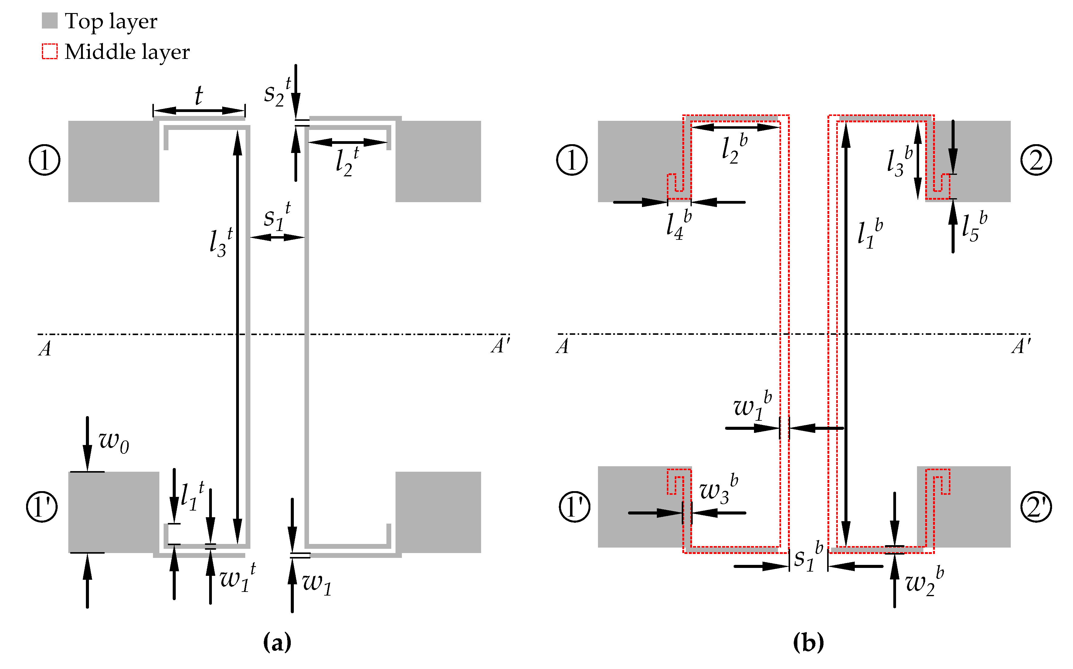
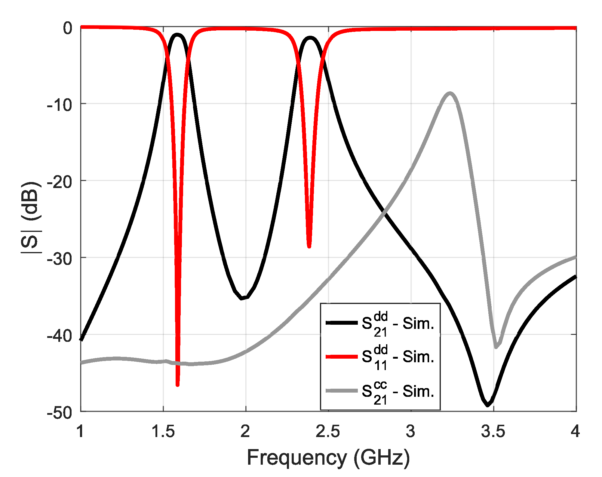
A 3-D view of the proposed multilayer structure for balanced dual-band operation is depicted in Figure 1. The two dimensional layout for each layer is depicted in Figure 2. The pattern etched on the top layer was used in [26] for the design of a single-band balanced BPF. It basically consists of a pair of open-loop resonators that are magnetically coupled (under DM operation). The middle layer also consists of a pair of open-loop resonators that are magnetically coupled when operating in DM. The difference between the two coupled resonant structures lies on the type of excitation and the values of the resonance frequencies. Thus, top layer resonators are excited via the gap capacitance associated with the gap width s 2 t , while the middle structure is excited by means of the broadside capacitance created between the top feeding lines and the middle layer conducting strips. Figure 3 illustrates the overlapping section between layers which originates the broadside capacitance (indicated by the shaded region). By setting the value of l over , it is possible to control the excitation level of the middle-layer resonators, which is critical to implement the response of the differential passband created by this pair of coupled resonators. Figure 4 plots the simulated electromagnetic response (simulations have been carried out using ADS Momentum from Keysight, stationed at Santa Rosa, California, United States of America, USA) of the entire multilayer structure for both DM and CM excitations. Two differential passbands with good CM rejection can be appreciated in such figure, demonstrating the expected behavior of the proposed structure. The design process of the multilayer balanced dual-band bandpass filter that leads to such response is described in detail in the next subsections.

2.2. Design Methodology

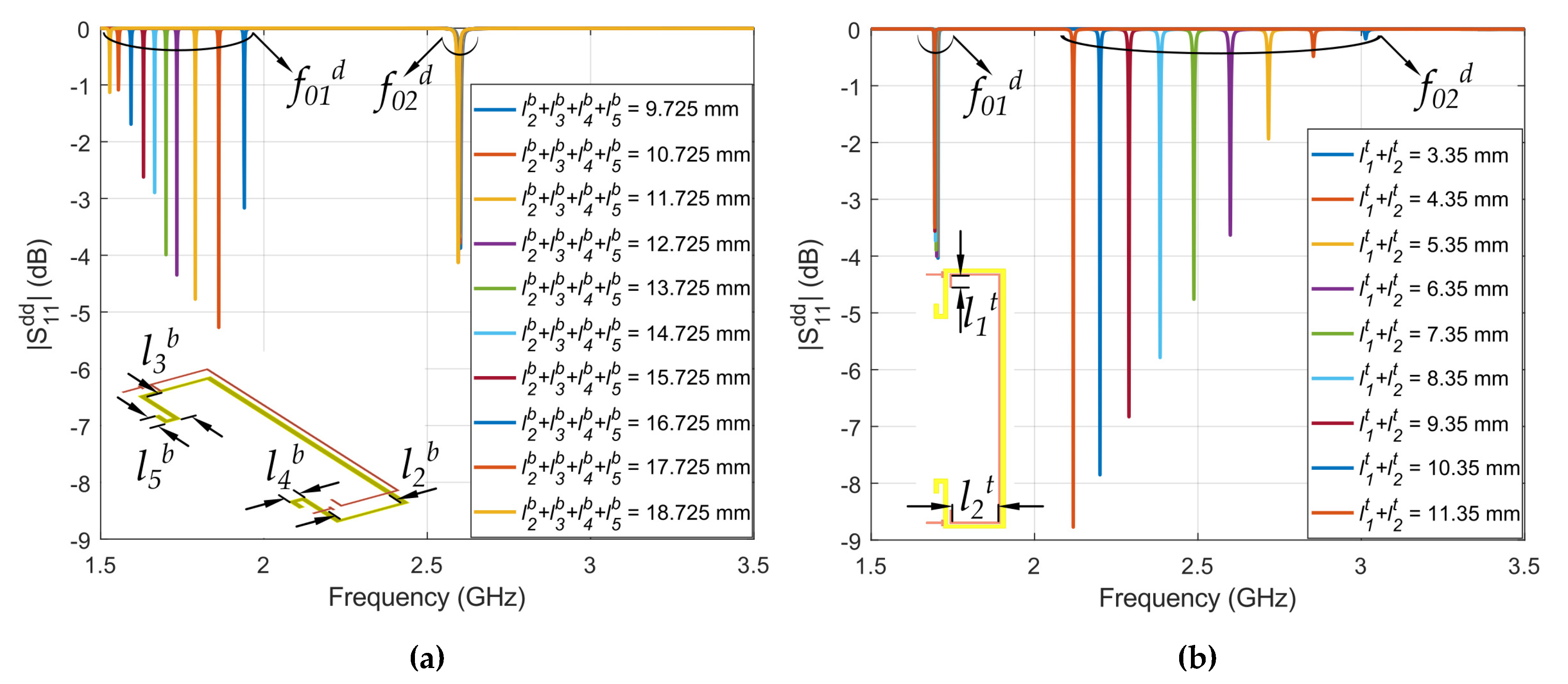
When designing a dual-band filter, it is very important that the two passbands can be independently tuned in terms of both center frequency and fractional bandwidth (FBW). In the case at hand, the first point that should be noted is that the middle layer of the structure introduces the lower passband, centered at f 01 d = 1.575 GHz, the L1 GPS signal frequency, while the top layer resonates at the first Wi-Fi band frequency, f 02 d = 2.45 GHz. This means that the upper frequency band should be allocated by setting the top layer parameters while lower frequency band must depend, exclusively, on the middle layer geometry. Let’s start by studying the resonance frequency of resonators in both layers. In Figure 5, the differential return loss, | S 11 d d | , have been represented when a single couple of top and middle resonators are weakly excited. The dips in the return loss correspond to the resonance frequencies of both resonators. Several parameters from each resonator were varied to show the dependence of those resonance frequencies with the resonator’s length. From the simulated results (Figure 5) the following conclusions can be inferred:
  • If middle layer resonators length is kept constant, changing top layer resonators length only affects the upper band center frequency, with very slight effect on the lower band center frequency.
  • If top layer resonators length is kept constant, changing middle layer resonators length only affects the lower band center frequency with negligible effect on the upper band center frequency.
From these results, it is clear that there is flexibility in locating the center frequencies of each passband as long as both frequencies are not very close to each other. In this latter case, resonators on both layers would interact significantly, thus leading to band-to-band dependence breaking the asynchronous behavior between the pair of resonators. This situation would not be desirable for designing purposes. Furthermore, the independence of the passbands is also related to the excitation mechanism of each resonator pair. As mentioned before, top layer resonators are mainly excited due to the electric field confined within the gap of width s 2 t (gap capacitance) while middle layer resonators are excited by means of the electric field concentrated between the feeding lines and the resonator conductor strips (broadside capacitance). This fact, together with the sufficient separation of the two center frequencies, leads to the desired independence exhibited when locating the center frequencies of the differential passbands.
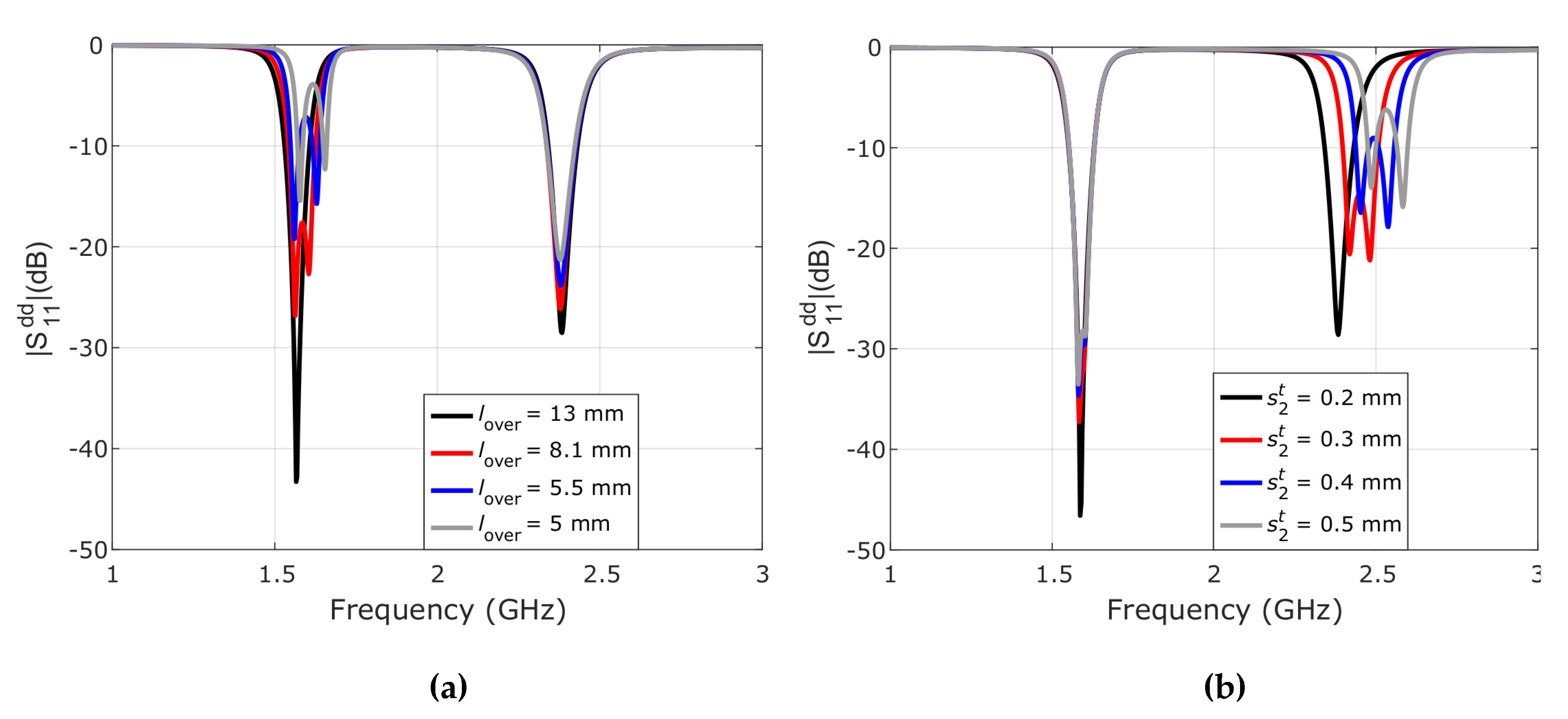
Once the independent control of the resonance frequencies has been demonstrated, the next electrical parameter to be considered in the design process is the correct excitation of the resonators to generate two properly matched differential passbands. In this regard, as mentioned above, the parameters that control top and middle layer resonators excitation are mainly s 2 t and l over , respectively. In order to investigate on the influence of such parameters on the matching level of both differential passbands, i.e., | S 11 d d | , Figure 6 shows the differential return loss of the two differential passbands as a function of s 2 t and l over . From this figure it is clear that l over mainly influences the reflection coefficient of the lower differential passband while s 2 t controls the reflection coefficient of the upper differential passband. Note that s 2 t slightly modifies the value of the upper center frequency. However, this problem can be solved by barely modifying some of the other dimensions of the top layers resonators in a very simple manner, as explained in [26]. Finally, the last step in the design process is to verify that the fractional bandwidth of the two differential passbands can be set independently. If this is the case, we have two totally independent differential passbands, which represents the ideal case when designing filters with dual-band operation.
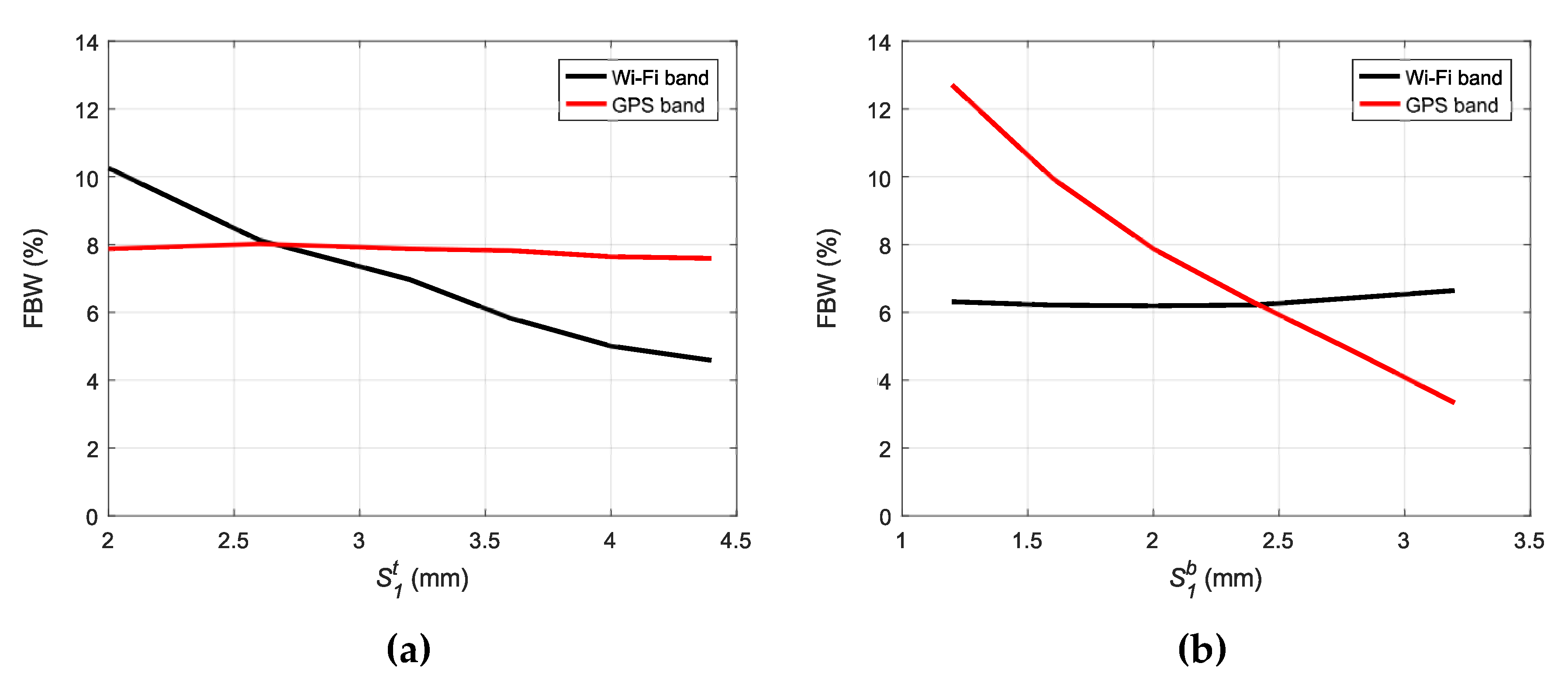
Fractional bandwidth is related to the coupling level between resonators. The closer the resonators are the larger the fractional bandwidth is. Referring to Figure 2, the relevant geometrical parameter that controls the coupling between resonators for the ones located on the top layer is s 1 t , whereas s 1 b is the responsible for the coupling level between resonators in the middle layer. To verify this, fractional bandwidth as a function of s 1 t and s 1 b are shown in Figure 7a,b, respectively. From Figure 7, it is clear that, as it happened with the center frequencies and the differential return loss, the fractional bandwidth of the two differential passbands are also independent from each other. This fact confers the designer full possibilities to adapt the design to other frequencies or other bandwidths that might be necessary for other requirements and specifications.
In order to clarify the design process of the balanced dual-band bandpass filter proposed in this paper, the following summary is given below:
  • First, resonator dimensions must be obtained in order to fit their resonance frequencies to the desired passband center frequencies. Since these specific resonators are half-wavelength open loop resonators, their resonance frequencies are mainly determined by their lengths, which can be easily obtained by using well known equations [45] or with the help of the electromagnetic simulator.
  • Next, the fractional bandwidth of each differential passband is set to the desired one by properly adjusting the values of s 1 t and s 1 b .
  • Finally, the matching level is adjusted by setting the values of s 2 t and l over .
The proposed filter is finally designed and ready to be fabricated and measured.

3. Results

3.1. Prototype Example

In this section, an example of differential dual-band BPF filter design is reported. The first passband corresponds to the L1 GPS signal at 1 . 575 GHz. A fractional bandwidth of 8.86% is considered. The second passband is designed to be allocated in the first Wi-Fi frequency at 2 . 45 GHz, with a fractional bandwidth of 5.69%. The filter is implemented on a substrate with the following features: dielectric constant ε r 1 = ε r 2 = 3 . 0 , and thicknesses h s u b = 1.016 mm. As explained in detail in previous sections, the first step in the design process is to obtain the resonator dimensions to set the two desired center frequencies, which are controlled by resonator lengths (recall that resonance arises when the length of the resonators is half the guided wavelength at the desired center frequencies). Once resonators are designed, design curves in Figure 6 and Figure 7 are used to set the desired matching level and fractional bandwidth. Following this procedure, the final dimensions of the proposed dual-band differential filter in Figure 2 are those of the caption of Figure 4, where we have represented the final simulated filter response. This figure exhibits two differential passbands well allocated. The common-mode rejection level is very satisfactory too. To verify experimentally these results, a prototype has been fabricated and measured. Results are presented in next subsection.

3.2. Experimental Results

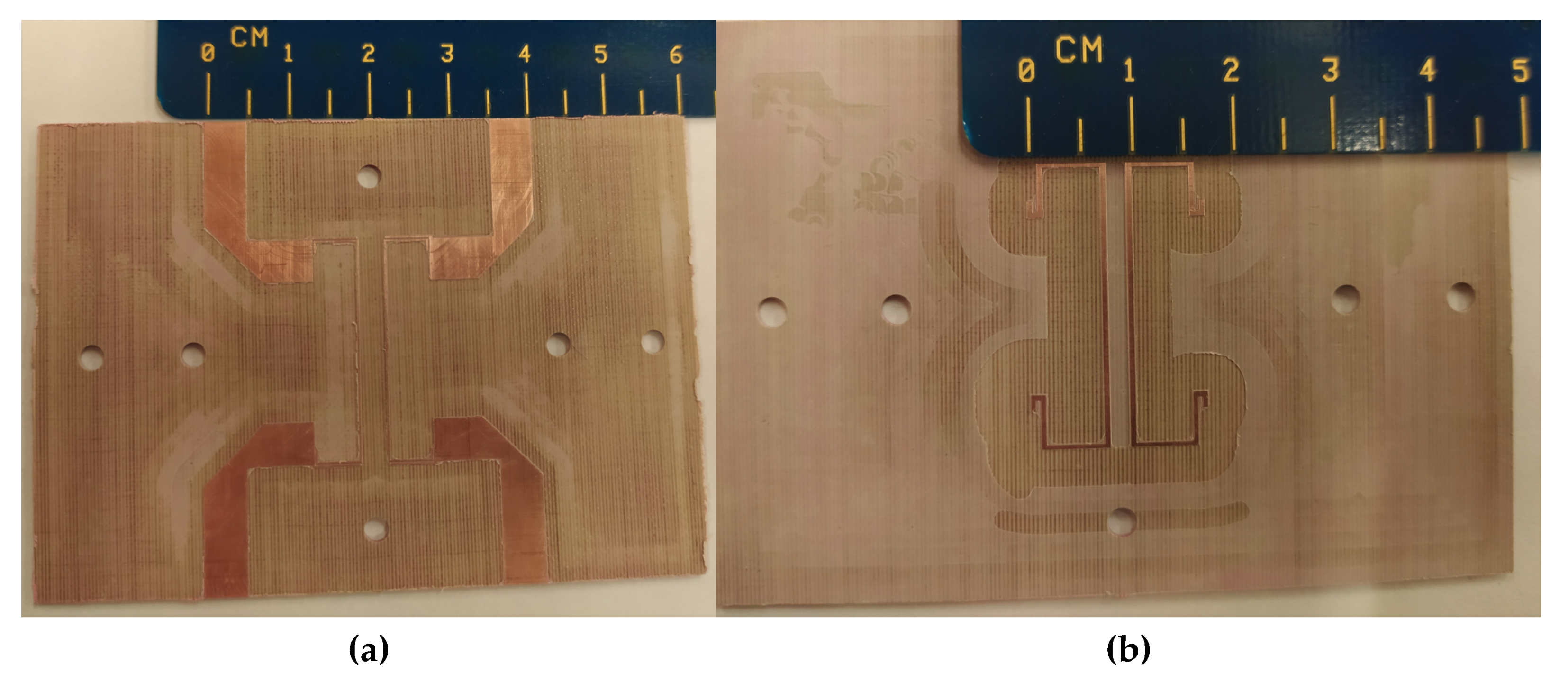
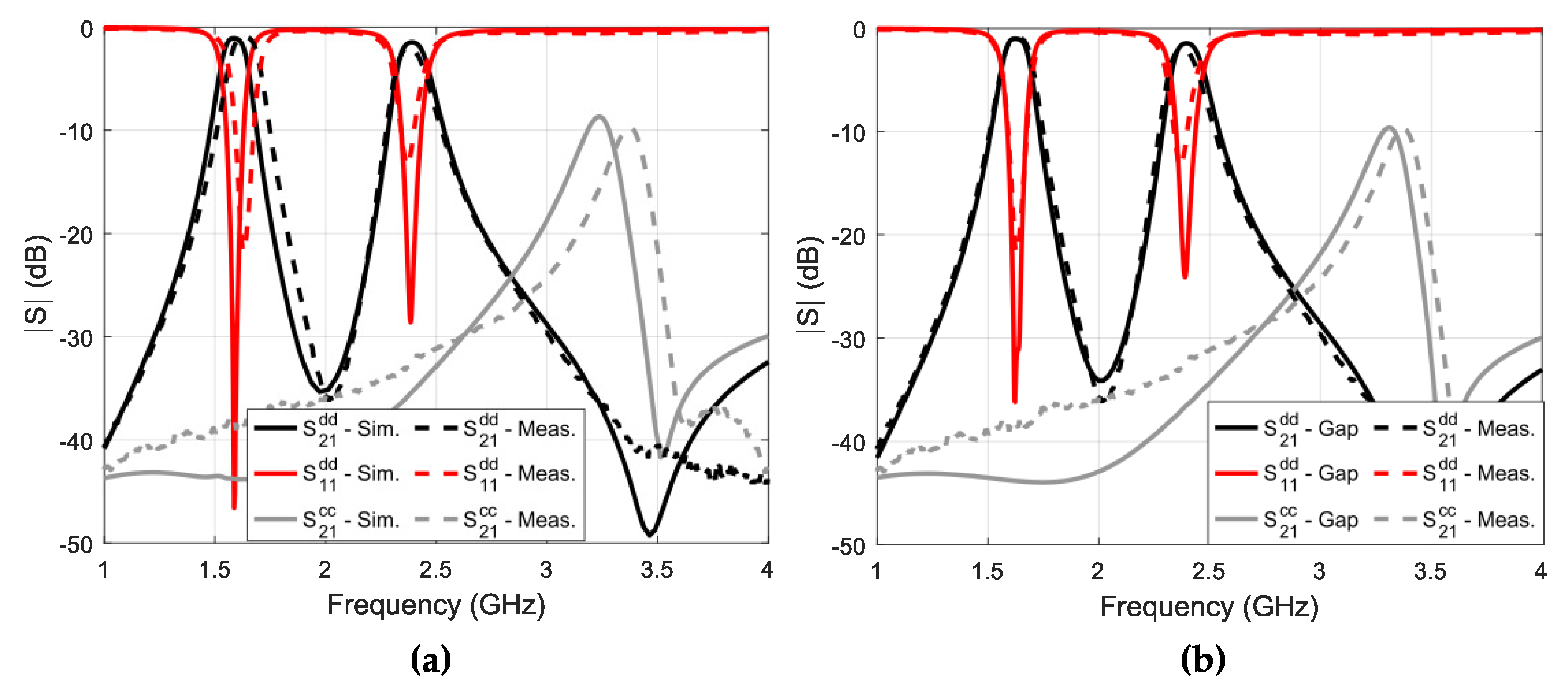
In this section, a comparison between the results of the electromagnetic simulations and the measurements of the manufactured prototype is carried out. Figure 8 shows a photograph of the fabricated prototype, which has been fabricated using a mechanical milling machine (LPKF S103 from LPKF Laser & Electronics, stationed at Garbsen, Germany). Measurements have been carried out using Agilent PNA-E8363B with a Test-Set N4420B extension (thus, with a 4-port system), both devices from Keysight, under normal conditions of pressure, temperature and humidity. This network analyzer has a single source, so the DM and CM have been obtained using the program Physical Layer Test System from Keysight that allows the user load calibrations and implement a transformation between the actually measured 4 × 4 scattering matrix of the 4-port single-ended circuit and the 2 × 2 differential-differential, common-common and differential-common 2 × 2 scattering matrices of the balanced 2-port system. Simulated and measured DM and CM responses are depicted in Figure 9. This figure shows a good agreement between simulated and measured results, although the measured lower band is slightly shifted when compared with the simulated one. This fact can be explained if we take into account that multilayer structures can suffer from the presence of small air gaps that may appear if layers are not perfectly stuck. Furthermore, the mechanical milling machine might sometimes remove a thin layer of the substrate, and this affects the effective dielectric constant of the substrate. This effect can be minimized using some suitable prepreg layer, which should be included in the simulations, of course. In order to verify the effect of this hypothesized air gap, the response of the differential filter has been simulated considering a 0.025 mm air gap between the stacked dielectric substrates. This response is depicted in Figure 9b. The results show a good agreement between simulations and measurements. The use of a low permittivity substrate has the puspose of reducing the air gap effect, since the closer the dielectric constant is to that of air, the less the effective permittivity will be affected. The use of low permittivity substrates will also decrease the capacitance between layers so that the cross coupling between resonators will also be lower. The measured results show a CM rejection level greater than 39 dB and 33 dB for the first and second DM passbands, respectively. Measured insertion loss at the first and second DM center frequencies is 0.9 dB and 1.9 dB respectively. In addition, band-to-band isolation is better than 36 dB, which is satisfactory for many practical applications.

4. Discussion

In order to illustrate the benefits of the proposed structure, a comparison between the proposal in this paper and a number of contributions available in the specialized literature is provided in Table 1.
In terms of the different relevant parameters, several conclusions can be inferred from the comparison between our design and those reported in the literature (Table 1):
  • Filter size. In terms of electrical size, the proposed filter is very competitive. Indeed, is one of the smallest in the table (0.035 λ g 2 , λ g being the guided wavelength at the center of the lower transmission band, when the average size for those presented in Table 1 is 0.184 λ g 2 ). There are only two designs smaller than the one in this contribution [40,42], but it should be taken into account that one of the main advantages of our filter lies on its simplicity. Size reduction through optimization of the geometry of the resonators would be possible but has not been attempted.
  • Fractional bandwidth. Our design confers the designer total and independent control on the bandwidth of the two passbands. For our specifications and requirements, the filter perfectly covers both the GPS band and the Wi-Fi band, so there are no issues on this regard. If we look at the results obtained in the considered literature, the average fractional bandwidth is 8.74% (first band) and 5.72% (second band). Both values are very close to those reported in this work. These values can still be increased a little further by adjusting the values of the separation between resonators, as it can be seen in Figure 7 in the paper. Note that using practicable values of such separations, our design would be able to compete with those with the highest values of FBW reported in Table 1.
  • Insertion loss. The average IL of the designs presented in Table 1 are 1.63 dB and 2.25 dB for the first and second passbands, respectively. Note that the measured IL values for our design is, once again, competitive with the state-of-the-art, providing one the lowest values of IL for the first passband.
  • Band-to-band isolation. The best way of obtaining good band-to-band isolation is to introduce one or more transmission zeros between the passbands. This is not the case in the presented design. Nevertheless, the IL in the frequency region between passbands reaches 36 dB, this being a very good value for many applications. Ten of the designs included in Table 1 exhibit transmission zeroes between passband. Thus, this point could be considered the main drawback of the proposed filter topology and adding elements to introduce transmission zeros would result into a significant improvement, provided the other relevant features of the filter are not significantly affected.
  • Common-mode Rejection Ratio (CMRR). The average CMRR values of the filters in Table 1 for the first and second differential passbands is 37.95 dB and 32.55 dB, respectively. These values are very close to the ones achieved with the proposed design. The advantage of our proposal is that this high level of CMRR is inherent to the coupling scheme and no additional components have to be added to enhance the CM suppression (such as lumped inductors, capacitors or resistors, additional CM rejection stages, additional open-circuit stubs, etc.). The introduction of these elements usually entails disadvantages (increase in complexity and the need of reaching a trade-off to avoid the deterioration of other filter parameters).
In brief, the design presented in this work is one of the smallest reported in the literature, it has low complexity and allows for easy configuration of the two passbands (both, center frequency and FBW). At the same time, leads to high CMRR values without relying on additional elements that might disrupt the differential-mode response. The main deawback of our proposal could be the lack of transmission zeroes in the frequency region between passbands. Nevertheless, the band-to-band isolation level presented in this work is satisfactory for most applications.

5. Conclusions

In this paper, a new dual-band balanced bandpass filter (DB-B-BPF) with inherent common-mode rejection is presented. The proposed structure is based on the use of two pairs of magnetically coupled open-loop resonators implemented in multilayer technology. The lower differential-mode (DM) passband is created by the middle layer resonators, while the upper DM passband is associated with the top layer resonators. By using this configuration, it is possible to design the two DM passbands with independent control of bandwidth and matching level. At the same time, very good band-to-band isolation and common-mode rejection is achieved. To demonstrate the usefulness of this proposal, an example of a filter operating for GPS and Wi-Fi applications (1.58 GHz and 2.4 GHz) was designed, fabricated and measured. Experiments show a Common-Mode Rejection Ratio (CMRR) better than 38 dB and 31.1 dB for the lower and upper DM passbands, respectively. Measured DM insertion loss for both passbands is 0.92/1.94 dB and the obtained 3-dB bandwidth is 8.86/5.69 %.

Author Contributions

J.L.M.d.R., A.L. and A.F.-P. designed, simulated, manufactured and measured the filter prototype. F.M., J.M. and A.J.M.-R. supervised the whole study. All the authors participated in writing the paper and in revising the article. All authors have read and agreed to the published version of the manuscript.

Funding

This work has been funded by the Spanish AEI Ministry of Science, Innovation and Universities and EU Feder Funds (project TEC2017-84724-P). J.M.R. acknowledges financial support of a research scholarship of the Spanish Ministry of Education (reference PRE2018-085677).

Conflicts of Interest

The authors declare no conflict of interest

References

  1. Eisenstant, W.R.; Stengel, B.; Thompson, B.M. Microwave Differential Circuit Design Using Mixed-Mode S-Parameters; Artech House: Boston, MA, USA, 2006. [Google Scholar]
  2. Martin, F.; Zhu, L.; Hong, J.; Medina, F. Balanced Microwave Filters; John Wiley & Sons: New York, NY, USA, 2018. [Google Scholar]
  3. Xia, B.; Wu, L.S.; Mao, J.F. A new balanced-to-balanced power divider/combiner. IEEE Trans. Microw. Theory Tech. 2012, 60, 2791–2798. [Google Scholar] [CrossRef]
  4. Xia, B.; Wu, L.S.; Ren, S.W.; Mao, J.F. A balanced-to-balanced power divider with arbitrary power division. IEEE Trans. Microw. Theory Tech. 2013, 61, 2831–2840. [Google Scholar] [CrossRef]
  5. Wu, L.S.; Guo, Y.X.; Mao, J.F. Balanced-to-balanced Gysel power divider with bandpass filtering response. IEEE Trans. Microw. Theory Tech. 2013, 61, 4052–4062. [Google Scholar] [CrossRef]
  6. Feng, W.; Zhu, H.; Che, W.; Xue, Q. Wideband in-phase and out-of-phase balanced power dividing and combining networks. IEEE Trans. Microw. Theory Tech. 2014, 62, 1192–1202. [Google Scholar] [CrossRef]
  7. Zhou, Y.; Deng, H.W.; Zhao, Y. Compact balanced-to-balanced microstrip diplexer with high isolation and common-mode suppression. IEEE Microw. Wirel. Compon. Lett. 2014, 24, 143–145. [Google Scholar] [CrossRef]
  8. Hsiao, C.Y.; Wu, T.L. A novel dual-function circuit combining high-speed differential equalizer and common-mode filter with an additional zero. IEEE Microw. Wirel. Compon. Lett. 2014, 24, 617–619. [Google Scholar] [CrossRef]
  9. Naqui, J.; Fernández-Prieto, A.; Durán-Sindreu, M.; Mesa, F.; Martel, J.; Medina, F.; Martín, F. Common mode suppression in microstrip differential lines by means of complementary split ring resonators: Theory and applications. IEEE Trans. Microw. Theory Tech. 2012, 60, 3023–3034. [Google Scholar] [CrossRef]
  10. Olvera-Cervantes, J.L.; Corona-Chávez, A. Microstrip balanced bandpass filter with compact size, extended-stopband and common-mode noise suppression. IEEE Microw. Wirel. Compon. Lett. 2013, 23, 530–532. [Google Scholar] [CrossRef]
  11. Horestani, A.K.; Durán-Sindreu, M.; Naqui, J.; Fumeaux, C.; Martín, F. S-shaped complementary split ring resonators and their application to compact differential bandpass filters with common-mode suppression. IEEE Microw. Wirel. Compon. Lett. 2014, 24, 149–151. [Google Scholar] [CrossRef] [Green Version]
  12. Wu, X.H.; Chu, Q.X.; Qiu, L.L. Differential wideband bandpass filter with high-selectivity and common-mode suppression. IEEE Microw. Wirel. Compon. Lett. 2013, 23, 644–646. [Google Scholar] [CrossRef]
  13. Lin, L.; Bao, J.; Du, J.J.; Wang, Y.M. Differential wideband bandpass filters with enhanced common-mode suppression using internal coupling techniquen. IEEE Microw. Wirel. Compon. Lett. 2014, 24, 300–302. [Google Scholar]
  14. Xu, X.; Wang, J.; Zhu, L. A new approach to design differential-mode bandpass filters on SIW structure. IEEE Microw. Wirel. Compon. Lett. 2013, 23, 635–637. [Google Scholar] [CrossRef]
  15. Feng, W.; Che, W. Novel wideband differential bandpass filters based on T-shaped structure. IEEE Trans. Microw. Theory Tech. 2012, 60, 1560–1568. [Google Scholar] [CrossRef]
  16. Wu, X.H.; Chu, Q.X. Compact differential ultra-wideband band-pass filter with common-mode suppression. IEEE Microw. Wirel. Compon. Lett. 2012, 22, 456–458. [Google Scholar] [CrossRef]
  17. Lu, Y.J.; Chen, S.Y.; Hsu, P. A differential-mode wideband bandpass filter with enhanced common-mode suppression using slotline resonator. IEEE Microw. Wirel. Compon. Lett. 2012, 22, 503–505. [Google Scholar] [CrossRef]
  18. Vélez, P.; Naqui, J.; Fernández-Prieto, A.; Durán-Sindreu, M.; Bonache, J.; Martel, J.; Medina, F.; Martín, F. Differential bandpass filter with common-mode suppression based on open split ring resonators and open complementary split ring resonators. IEEE Microw. Wirel. Compon. Lett. 2013, 23, 22–24. [Google Scholar] [CrossRef]
  19. Feng, W.; Che, W.; Ma, Y.; Xue, Q. Compact wideband differential bandpass filters using half-wavelength ring resonator. IEEE Microw. Wirel. Compon. Lett. 2013, 23, 81–83. [Google Scholar] [CrossRef]
  20. Shi, J.; Shao, C.; Chen, J.X.; Lu, Q.Y.; Peng, Y.; Bao, Z.H. Compact low-loss wideband differential bandpass filter with high common-mode suppression. IEEE Microw. Wirel. Compon. Lett. 2013, 23, 480–482. [Google Scholar] [CrossRef]
  21. Wu, C.H.; Wang, C.H.; Chen, C.H. Novel balanced coupled-line bandpass filters with common-mode noise suppression. IEEE Trans. Microw. Theory Tech. 2007, 55, 287–295. [Google Scholar] [CrossRef]
  22. Wu, C.H.; Wang, C.H.; Chen, C.H. Stopband-extended balanced bandpass filter using coupled stepped-impedance resonators. IEEE Microw. Wirel. Compon. Lett. 2007, 17, 507–509. [Google Scholar] [CrossRef]
  23. Lin, S.C.; Yeh, C.Y. Stopband-extended balanced filters using both λ/4 and λ/2 SIRs with common mode suppression and improved passband selectivity. Prog. Electromagn. Res. 2012, 128, 215–228. [Google Scholar] [CrossRef] [Green Version]
  24. Shi, J.; Chen, J.; Tang, H.; Zhou, L. Differential bandpass filter with high common-mode rejection ratio inside the differential-mode passband using controllable common-mode transmission zero. In Proceedings of the 2013 IEEE International Wireless Symposium (IWS), Beijing, China, 14–18 April 2013. [Google Scholar] [CrossRef]
  25. Wang, H.; Tam, K.W.; Ho, S.K.; Kang, W.; Wu, W. Short-ended self-coupled ring resonator and its application for balanced filter design. IEEE Microw. Wirel. Compon. Lett. 2014, 24, 312–314. [Google Scholar] [CrossRef]
  26. Fernández-Prieto, A.; Lujambio, A.; Martel, J.; Medina, F.; Mesa, F.; Boix, R. Simple and Compact Balanced Bandpass Filters Based on Magnetically Coupled Resonators. IEEE Trans. Microw. Theory Tech. 2015, 63, 1843–1853. [Google Scholar] [CrossRef]
  27. Shi, J.; Xue, Q. Balanced Bandpass Filters Using Center-Loaded Half-Wavelength Resonators. IEEE Trans. Microw. Theory Tech. 2010, 58, 970–977. [Google Scholar]
  28. Shi, J.; Xue, Q. Dual-Band and Wide-Stopband Single-Band Balanced Bandpass Filter With High Selectivity and Common-Mode Suppression. IEEE Trans. Microw. Theory Tech. 2010, 58, 2204–2212. [Google Scholar] [CrossRef]
  29. Guo, X.; Zhu, L.; Wu, W. Balanced Wideband/Dual-Band BPFs on a Hybrid Multimode Resonator with Intrinsic Common-Mode Rejection. IEEE Trans. Microw. Theory Tech. 2016, 64, 1997–2005. [Google Scholar] [CrossRef]
  30. Gómez-García, R.; Muñoz-Ferreras, J.-M.; Feng, W.; Psychogiou, D. Balanced Symmetrical Quasi-Reflectionless Single-and Dual-Band Bandpass Planar Filters IEEE Microw. Wirel. Compon. Lett. 2018, 28, 798–800. [Google Scholar] [CrossRef]
  31. Fernández-Prieto, A.; Martel, J.; Medina, F.; Mesa, F.; Qian, S.; Hong, J.; Naqui, J.; Martín, F. Dual-Band Differential Filter using Broadband Common-Mode Rejection Artificial Transmission Line. Prog. Electromagn. Res. 2013, 139, 779–797. [Google Scholar] [CrossRef] [Green Version]
  32. Bagci, F.; Fernández-Prieto, A.; Lujambio, A.; Martel, J.; Bernal, J.; Medina, F. Compact Balanced Dual-Band Bandpass Filter Based on Modified Coupled-Embedded Resonators. IEEE Microw. Wirel. Compon. Lett. 2017, 27, 31–33. [Google Scholar] [CrossRef]
  33. Shi, J.; Xue, Q. Novel Balanced Dual-Band Bandpass Filter Using Coupled Stepped Impedance-Resonators. IEEE Microw. Wirel. Compon. Lett. 2010, 20, 19–21. [Google Scholar]
  34. Lee, C.H.; Hsu, C.I.G.; Hsu, C.C. Balanced Dual-Band BPF with Stub-Loaded SIRs for Common-Mode Suppression. IEEE Microw. Wirel. Compon. Lett. 2010, 20, 70–72. [Google Scholar] [CrossRef]
  35. Wang, K.; Zhu, L.; Wong, S.W.; Chen, D.; Guo, Z.C. Balanced dual-band BPF with intrinsic common-mode suppression on double-layer substrate. Electron. Lett. 2015, 51, 705–707. [Google Scholar] [CrossRef]
  36. Cho, Y.H.; Yun, S.W. Design of Balanced Dual-Band Bandpass Filters Using Asymmetrical Coupled Lines. IEEE Trans. Microw. Theory Tech. 2013, 61, 2814–2820. [Google Scholar] [CrossRef]
  37. Li, P.; Chu, H.; Zhao, D.; Chen, R.S. Compact Dual-Band Balanced SIW Bandpass Filter With Improved Common-Mode Suppression. IEEE Microw. Wirel. Compon. Lett. 2017, 27, 347–349. [Google Scholar] [CrossRef]
  38. Yang, L.; Choi, W.W.; Tam, K.W.; Zhu, L. Balanced Dual-Band Bandpass Filter With Multiple Transmission Zeros Using Doubly Short-Ended Resonator Coupled Line. IEEE Microw. Wirel. Compon. Lett. 2015, 63, 2225–2232. [Google Scholar] [CrossRef]
  39. Wei, F.; Guo, Y.J.; Qin, P.Y.; Shi, X.W. Compact Balanced Dual- and Tri-band Bandpass Filters Based on Stub Loaded Resonators. IEEE Microw. Wirel. Compon. Lett. 2015, 25, 76–78. [Google Scholar] [CrossRef]
  40. Song, Y.; Liu, H.; Zhao, W.; Wen, P.; Wang, Z. Compact Balanced Dual-Band Bandpass Filter With High Common-Mode Suppression Using Planar Via-Free CRLH Resonator. IEEE Microw. Wirel. Compon. Lett. 2018, 28, 996–998. [Google Scholar] [CrossRef]
  41. Hong, J.S. Microstrip Filters for RF/Microwave Applications; John Wiley & Sons: New York, NY, USA, 2011. [Google Scholar]
  42. Fernández-Prieto, A.; Martel, J.; Ugarte-Parrado, P.J.; Lujambio, A.; Martínez-Ros, A.J.; Martín, F.; Medina, F.; Boix, R.R. Compact balanced dual-band bandpass filter with magnetically coupled embedded resonators. IET Microw. Antennas Propag. 2019, 13, 492–497. [Google Scholar] [CrossRef]
  43. Fernández-Prieto, A.; Lujambio, A.; Martel, J.; Medina, F.; Martín, F.; Boix, R.R. Compact Balanced-to-Balanced Diplexer Based on Split-Ring Resonators Balanced Bandpass Filters. IEEE Microw. Wirel. Compon. Lett. 2018, 28, 218–220. [Google Scholar] [CrossRef]
  44. Fernández-Prieto, A.; Lujambio, A.; Martel, J.; Medina, F.; Martín, F.; Boix, R.R. Balanced-to-Balanced Microstrip Diplexer Based on Magnetically Coupled Resonators. IEEE Access 2018, 6, 18536–18547. [Google Scholar] [CrossRef]
  45. Makimoto, M.; Yamahista, S. Microwave Resonators and Filters for Wireless Communication. Theory, Design and Application; Springer: New York, NY, USA, 2001. [Google Scholar]
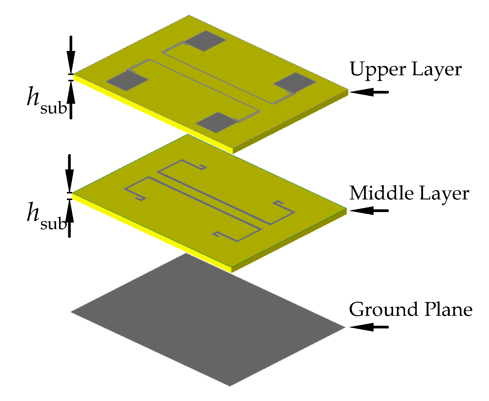
Figure 1. Deployed 3-D view of the proposed planar multilayer balanced dual-band bandpass filter.
Applsci 10 03113 g001
Figure 2. 2-D view of the two printed planes of the structure (not to scale). (a) Top layer; (b) Middle layer.
Applsci 10 03113 g002
Figure 3. Detailed view of the broadside capacitance involved in the feeding of middle layer resonators.
Applsci 10 03113 g003
Figure 4. Simulated response of the proposed multilayered balanced dual-band bandpass filter. The dimensions (in mm) used for the structure in Figure 2 that give rise to this response are: (i) top layer: t = 5 . 8 , w 0 = 5 . 1 , w 1 = 0 . 2 , w 1 t = 0 . 2 , l 1 t = 1 . 3 , l 2 t = 5 . 05 , l 3 t = 26 . 6 , s 1 t = 0 . 2 ; (ii) middle layer: w 1 b = 0 . 55 , w 2 b = 0 . 4 , w 3 b = 0 . 5 , l 1 b = 27 . 2 , l 2 b = 5 . 7 , l 3 b = 4 . 95 , l 4 b = 1 . 5 , l 5 b = 1 . 575 , s 1 b = 2 .
Applsci 10 03113 g004
Figure 5. Differential excitation return loss ( | S 11 d d | ) of the structure composed by a couple of top and middle resonators like those depicted in the insets when they are weakly excited: (a) l 2 b + l 3 b + l 4 b + l 5 b is varied; (b) l 1 t + l 2 t is varied. In both figures, the remaining physical parameters (see Figure 2) have been kept constant.
Applsci 10 03113 g005
Figure 6. | S 11 d d | for different values of (a) l over and (b) s 2 t .
Applsci 10 03113 g006
Figure 7. FBW with as a function of the resonators gap: (a) s 1 t is adjusted; (b) s 1 b is adjusted.
Applsci 10 03113 g007
Figure 8. Photograph of the manufactured prototype: (a) Top layer; (b) middle layer.
Applsci 10 03113 g008
Figure 9. Simulated and measured response of the proposed dual-band bandpass filter: (a) without gap; (b) with an air gap of 0.025 mm.
Applsci 10 03113 g009
Table 1. Comparison with reported balanced dual-band bandpass filters.
Ref.Size ( λ g × λ g ) *Differential-ModeCommon-Mode
f 0 d ( GHz )3-dB FBW (%)IL @ f 0 d (dB)B-to-B IL > 30 dBCMRR @ f 0 d (dB) | S 21 cc | > 30dB
[27]0.187 × 0.2851.84/2.459.2/8.22.2/2.62–2.320.5/20<30 dB
[28]0.314 × 0.4132.46/5.5618.7/9.50.96/1.93.05–550/37.5Up to 6.75 GHz
[29]N/A2.44/5.1918/8.71.14/2.053.6–4.141.26/40.35Up to 7 GHz
[30]0.275 × 0.132.82/3.215.2/5.11.9/1.7<30 dB13.6/7.83.2–3.24 GHz
[31]0.261 × 0.1732.5/5.2711/3.981.46/2.223.4/4.838.5/22.9(2–4.5)/(5.3–7.3) GHz
[32]0.153 × 0.2682.5/5.65.1/4.81.29/1.973.05–4.834.7/24.12.3–2.7 GHz
[33]0.259 × 0.5922.44/5.5716.4/8.621.78/2.533.15–4.736.2/31.1(1–5.75)/(6.2–8) GHz
[34]0.417 × 0.3772.44/5.258.61/4.572.4/2.821.8–3.852.6/42.2Up to 7 GHz
[35]N/A1.9/2.82.1/3.92.05/2.65<30 dB40/35.2Up to 3.2 GHz
[36]0.5 × 0.22.4/3.578.33/5.60.87/1.92.9–3.2824/29.1(1.5–2.32)/(2.45–2.9)/ (3–3.6) GHz
[37]1.23 × 1.233.5/5.243.14/3.821.52/1.653.7–4.7553.48/48.35Up to 6 GHz
[38]0.67 × 0.320.9/2.493.6/2.12.67/4.651.1–2.327.3/35.4Up to 4.3 GHz
[39]0.15 × 0.372.5/5.812.9/4.50.77/1.56<30 dB41.23/36.44(1–3)–(5.8–6.8) GHz
[40]0.131 × 0.1612.38/3.591.33/2.131.34/1.032.46–3.4948.6/49Up to 6 GHz
[42]0.137 × 0.1732.45/5.67.35/10.392.78/2.853–4.4547.2/30.2(1–3.81)/(5.22–7) GHz
This work0.237 × 0.1481.64/2.378.86/5.690.92/1.941.93–2.1338/31.1Up to 2.62 GHz
* Guided wavelength ( λ g ) at lowest frequency of operation ( f 0 d ).