Article

Double Spectral Electromagnetically Induced Transparency Based on Double-Bar Dielectric Grating and Its Sensor Application

1
Guangxi Key Laboratory of Multimedia Communications and Network Technology, School of Computer, Electronics and Information, Guangxi University, Nanning 530004, China
2
Center of Material Science, National University of Defense Technology, Changsha 410073, China
*
Authors to whom correspondence should be addressed.
Appl. Sci. 2020, 10(9), 3033; https://doi.org/10.3390/app10093033
Submission received: 26 March 2020 / Revised: 18 April 2020 / Accepted: 24 April 2020 / Published: 27 April 2020
(This article belongs to the Special Issue Recent Advances and Future Trends in Nanophotonics)

Abstract

:
The realization of the electromagnetically induced transparency (EIT) effect based on guided-mode resonance (GMR) has attracted a lot of attention. However, achieving the multispectral EIT effect in this way has not been studied. Here, we numerically realize a double EIT-ike effect with extremely high Q factors based on a GMR system with the double-bar dielectric grating structure, and the Q factors can reach 35,104 and 24,423, respectively. Moreover, the resonance wavelengths of the two EIT peaks can be flexibly controlled by changing the corresponding structural parameters. The figure of merit (FOM) of the dual-mode refractive index sensor based on this system can reach 571.88 and 587.42, respectively. Our work provides a novel method to achieve double EIT-like effects, which can be applied to the dual mode sensor, dual channel slow light and so on.

1. Introduction

In the past few decades, the electromagnetically induced transparency (EIT) effect caused by quantum destructive interference between two different excitation paths in a three-level atomic system has attracted extensive and in-depth research [1,2]. The EIT effect is that under the effect of strong resonance coupling light, the opaque medium becomes transparent for weak probe light and is accompanied by extraordinarily steep dispersion. In other words, the resonance probe light can propagate through the medium without being absorbed [3]. EIT has potential applications in many fields, such as sensing [4,5,6], slow light [5,7], nonlinear optics [8] and cavity quantum electrodynamics [9]. However, the realization of the EIT effect in atomic systems requires extremely strict experimental conditions, which limits its practical application. Therefore, researchers have turned to classical optical systems to achieve EIT-like effects. G. Shevts and J.S Wertele described the EIT analog in a classic plasma [10], and more of an EIT-like effect was subsequently observed in the plasmonic metamaterial [11,12]. The EIT-like effect has also been successfully achieved in other optical systems, such as waveguide cavity structures [13,14] and photonic crystals [15]. Sun-Goo Lee’s group realized the EIT-like effect based on the guided-mode resonance (GMR) effect for the first time in 2015 [16], the system consists of two planar dielectric waveguides and a subwavelength grating and a narrow transparent window appears in the transmission dip when high Q and low Q resonant waveguide modes are coupled.
In recent years, the realization of the EIT-like effect based on GMR has attracted more and more interest of researchers. Sun-Goo Lee’s group successfully realizes the polarization-independent EIT-like effect in two photonic systems, which are both composed of two planar dielectric waveguides and a two-dimensional photonic crystal [17]. Sun Y and Chen H et al. reported a planar metamaterial based on GMR achieve the EIT-like effect with a Q value exceeding 7000 [18]. Han Y and Yang et al. reported that a GMR system with two subwavelength silicon grating waveguide layers achieves the EIT-like effect with an ultra-high Q factor of 288,892 [19]. However, as is known to us, the realization of multispectral EIT effects by the subwavelength grating structure based on GMR has not been studied according to available works.
In this work, we numerically simulate the double spectral EIT-like effect in a coupled GMR system that consists of two silicon grating waveguide layers (GWLs) on a SiO2 substrate. In addition, both GWLs contain double-bar dielectric gratings with unequal lengths in a cycle. When the distance between the two GWLs meets the phase matching condition, the GMR system works as a Fabry–Perot (F–P) cavity and GWLs as the reflection boundary of the cavity thus two EIT peaks appear in the near infrared band due to the top GMR mode and the bottom GMR mode are intercoupled. The effects of two grating widths and the separation between the two gratings are also studied. After the structural parameters optimization, two EIT peaks present ultra-narrow FWHMs of 10 2 nm and ultra-high Q factors of 10 4 . In terms of the sensor, this system has ordinary sensitivity and high figure of merit (FOM) with compact structure and a simple manufacturing process. This double spectral EIT-like effect may not only be applied to the sensor, but also to slow light and nonlinear optics.

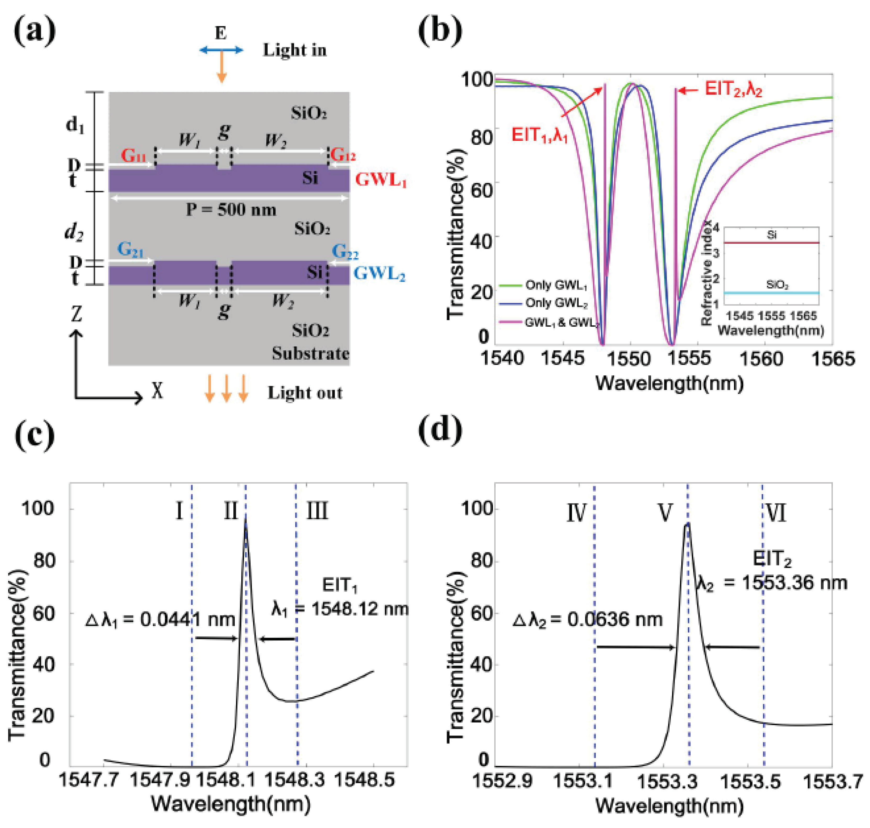
2. Structure and Simulation

The 3D finite-difference time-domain (FDTD) method was used to study the phenomenon of this optical system. During the simulation with FDTD, the mesh accuracy was set to λ/34 to ensure the convergence of the simulated results. The schematic of the GMR system with a double-bar dielectric grating structure is shown in Figure 1a. In terms of boundary conditions, X and Y were set to periodic, and Z was the perfectly matched layer (PML). The mesh accuracy in GWL1 and GWL2 were Δx = Δy = 5 nm and Δz = 10 nm, respectively. The inset of Figure 1b shows the real part of the refractive index value for SiO2 [20] and Si [21] as a function of the wavelength. The background index of the system was ns = 1.
Light polarized in the X direction (TM polarization) incidents vertically above the system in the near-infrared spectral band. The period P of grating was 500 nm. A SiO2 layer with a thickness of 1885 nm was designed on the top of the GMR structure in order to reduce the reflection of light. The distance (d2) between the two GWLs was designed to be 2137 nm. Gratings G11 and G12 had the same depths of D = 55 nm, and different widths of W1 = 100 nm and W2 = 230 nm, respectively. The separation between two Si gratings was g = 30 nm. The Si waveguide thickness was t = 435 nm. Meanwhile, structural parameters of GWL1 and GWL2 were consistent.

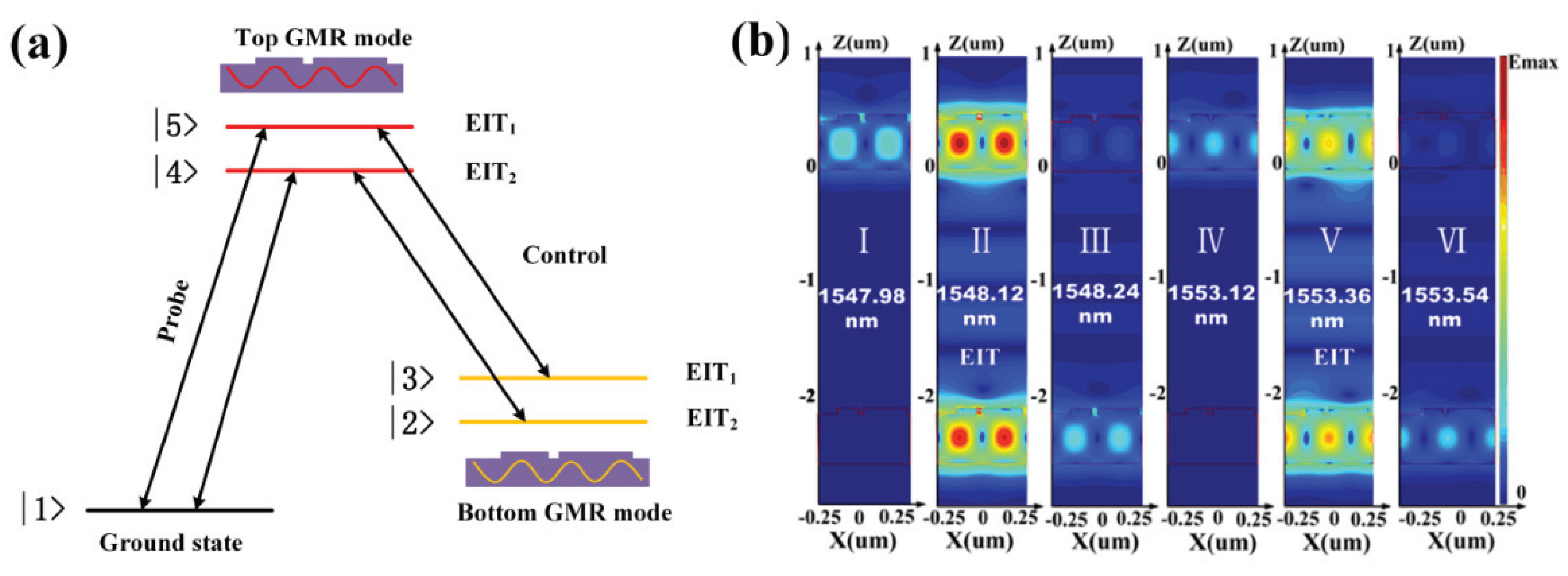
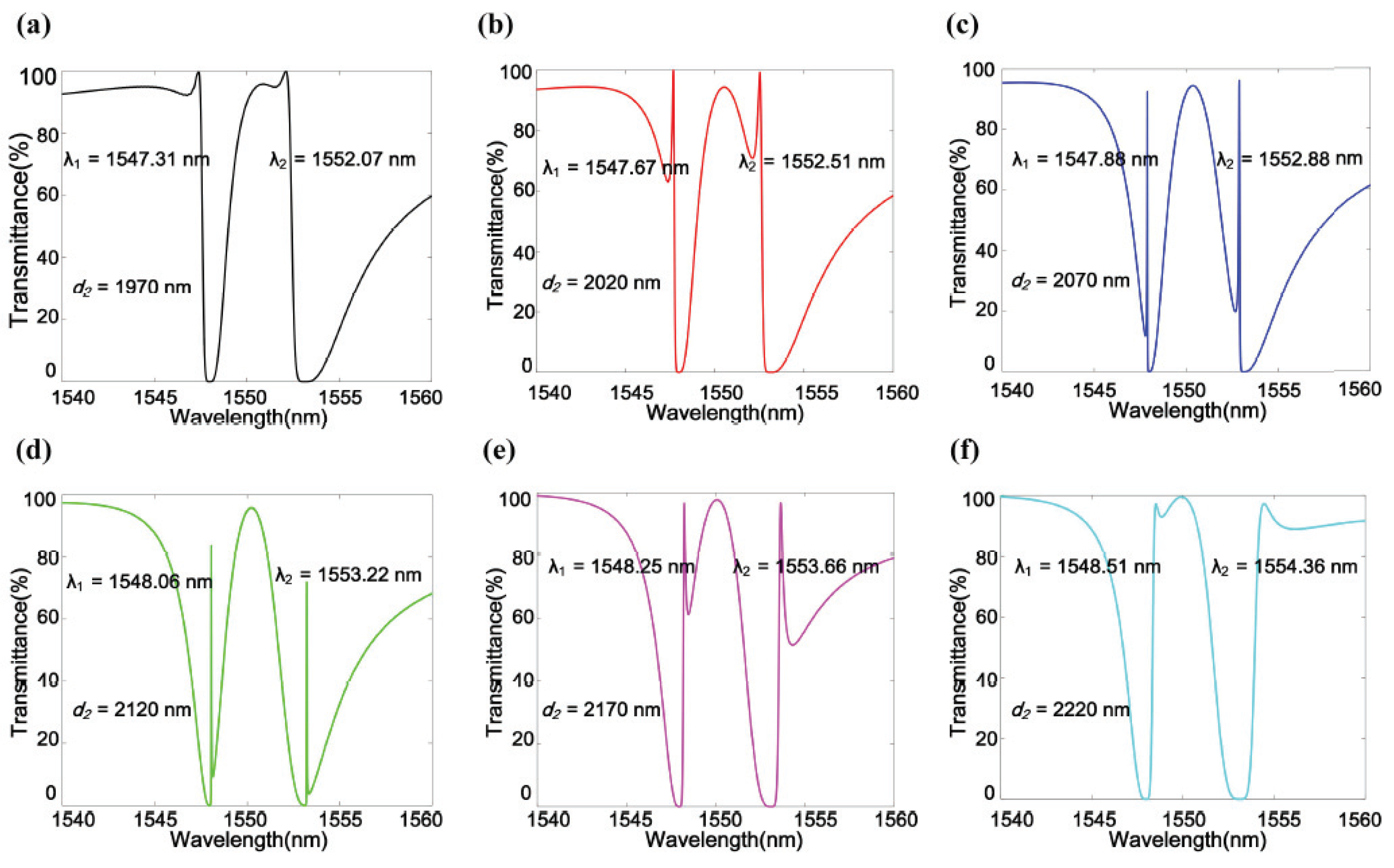
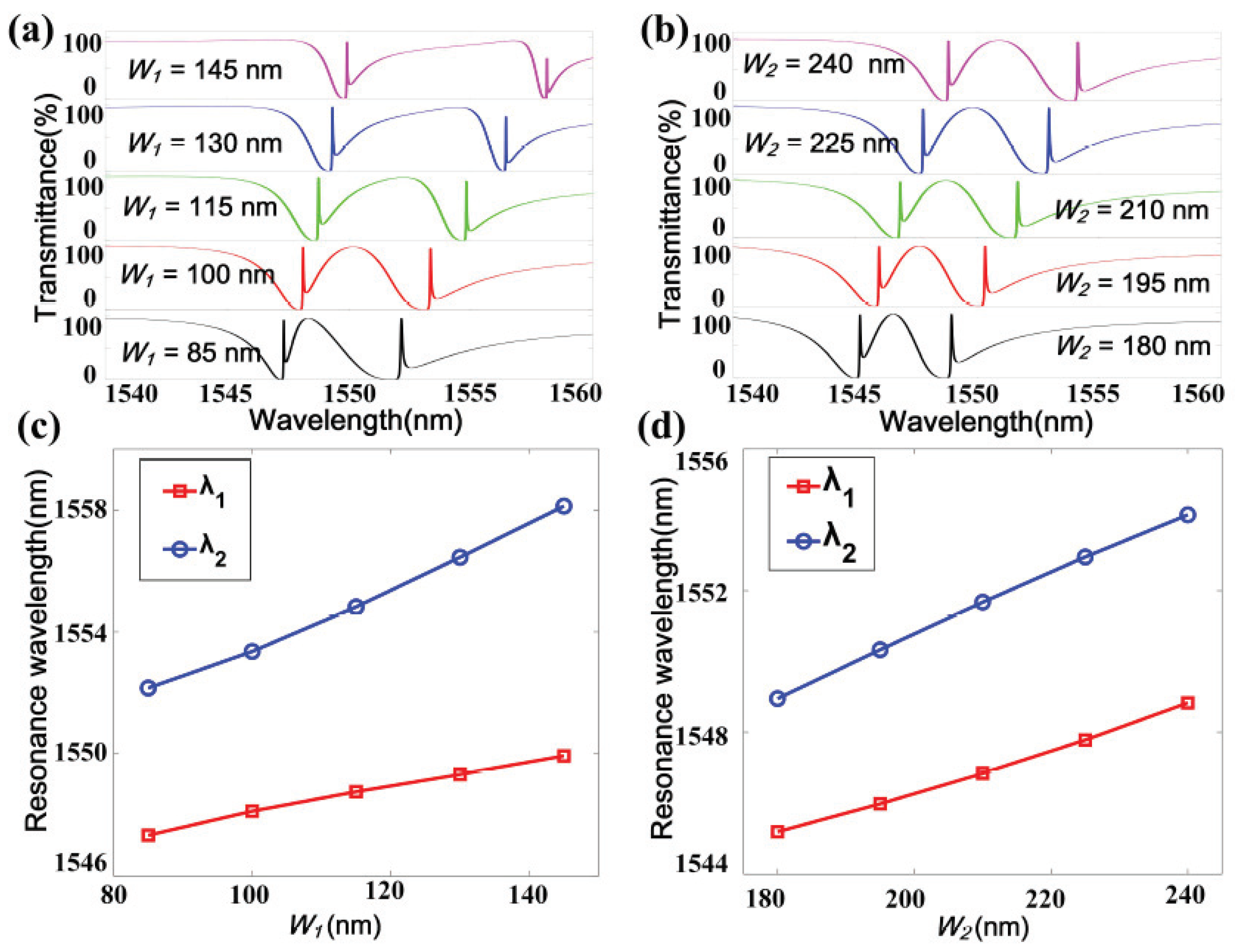
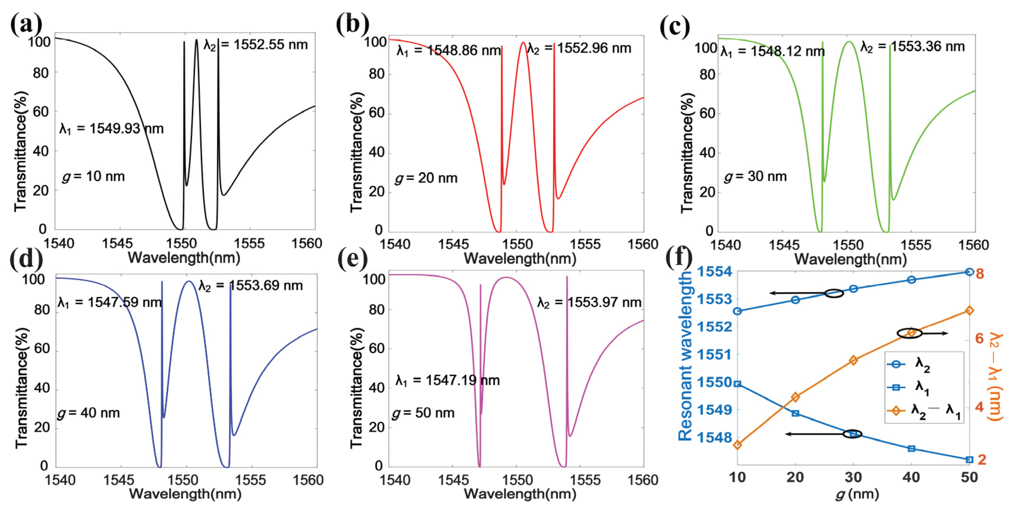
3. Results and Discussion
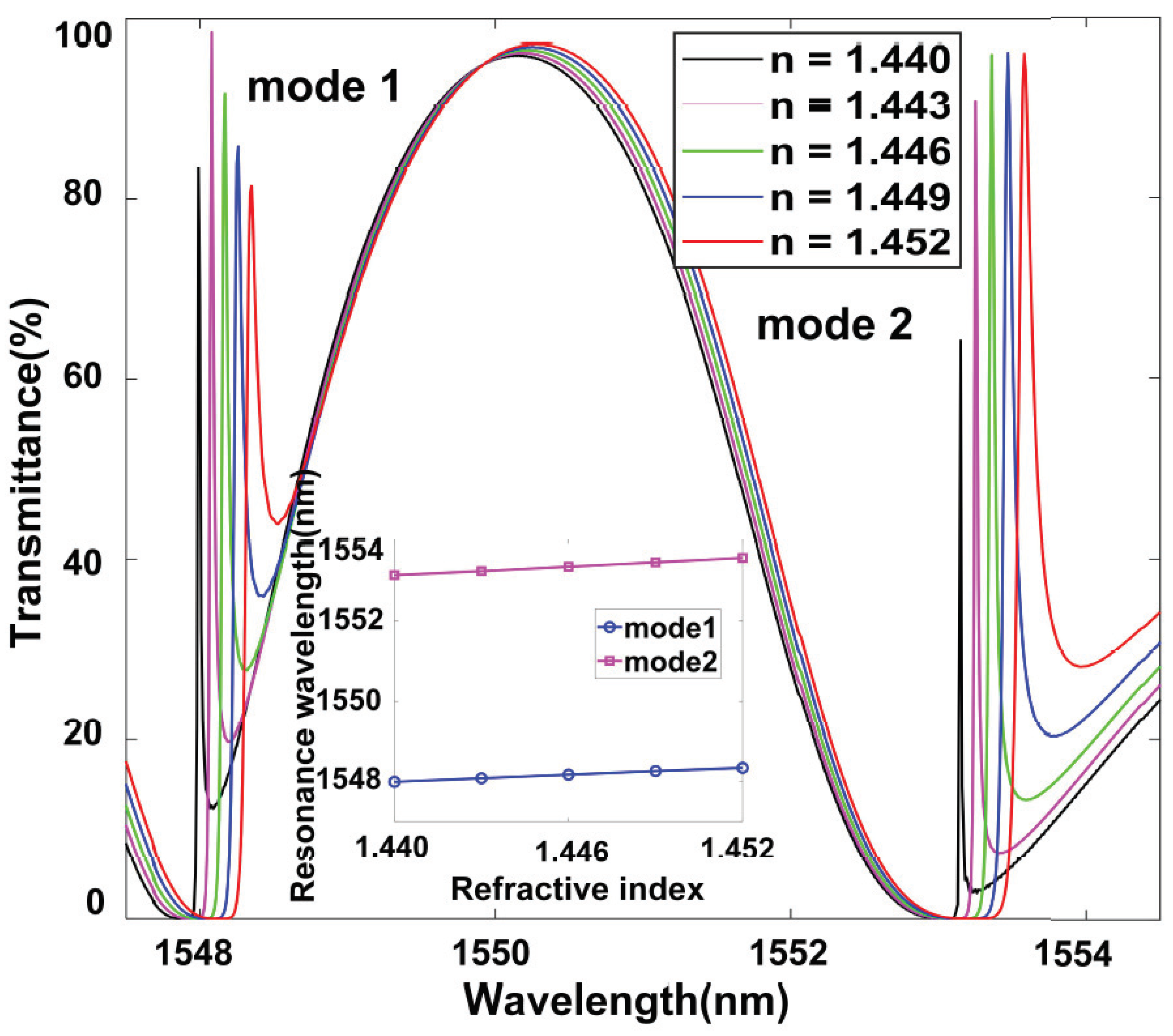
We first calculated the transmission spectrum of the structure with only single GWL1 (GWL2), as the green solid line (blue solid line) shown in Figure 1b. It is clear that the two different transmission dips appeared at the wavelengths of 1547.97 nm and 1553.08 nm. GWL1 and GWL2 had the same structure, but their optical properties were easily affected by the surrounding medium, thus the transmission spectra were slightly different. The SiO2 cover layer had an influence on the resonance frequency. Adding a SiO2 cover layer can reduce the impact of the surrounding medium on its optical characteristics to reach the same resonance frequency [18].
When GWL1 and GWL2 are both present, and their distance (d2) met the phase matching conditions, the top GMR mode (in GWL1) and the bottom GMR mode (in GWL2) were intercoupled, Therefore, two different sharp EIT resonances appear in the two resonance dips respectively due to destructive interference [12,19,22]. The transmission spectrum is shown by the solid red line in Figure 1b. We refer to the two EIT peaks as EIT1 and EIT2. The transmission characteristics of their magnified views are shown in Figure 1c,d, respectively. The resonance wavelengths of EIT11) and EIT22) were 1548.12 nm and 1553.36 nm, respectively, and their corresponding full width at half maximum (FWHM) was 0.0441 nm (∆λ1 in Figure 1c) and 0.0636 nm (∆λ2 in Figure 1d). The Q factor was an important parameter of the resonant cavity, which is defined as follows:
Q = λ FWHM
There, their corresponding Q factors reached 35,104 and 24,423, respectively. Obviously, our work has two higher Q factors than another double EIT-like effects work, which has two Q factors of 950 and 216 [6].
The analogy between our system and the atomic EIT system can help us understand the physics of the double EIT-like effect [23,24]. A double-Λ five-level model of the double EIT-like effect in our system is illustrated in Figure 2a. In the system, |1〉 represents the ground state, the field of the bottom GMR mode corresponds to the probability amplitudes of atoms in the metastable states |2〉 and |3〉, the field of the top GMR mode corresponds to the probability amplitudes of atoms in the excited states |4〉 and |5〉 [19,23,25]. The control field refers to the coupling between the top GMR mode and the bottom GMR mode, and the probe field refers to the input of the top GMR mode. We observed that two sharp EIT-like windows appeared in the probe area due to the introduction of the control field. The energy level of |5〉 — |1〉 was higher than |4〉 — |1〉, hence EIT1 corresponded to the destructive interference between two different transition pathways |1〉 → |5〉 and |1〉 → |5〉 → |3〉 → |5〉, EIT2 corresponded to the destructive interference between two different transition pathways |1〉 → |4〉 and |1〉 → |4〉 → |2〉 → |4〉.
In order to help us understand the origin of the double EIT-like effect in this GMR system, electric field distribution diagrams of the GMR system near two EIT peaks (such as the transmission spectra of Figure 1c,d are given in Figure 2b. Near the EIT1, electric field distribution at the off—resonant wavelength of EIT1 1547.98 nm (the blue dash I in Figure 1c) and 1548.24 nm (the blue dash III in Figure 1c) was very easily observed and excitation mainly occurred in GWL1 (I in Figure 2b) or GWL2 (III in Figure 2b), which was consistent with the characteristics of GMR. The corresponding transmittance was very low since the GMR mode was easily coupled to electromagnetic waves in free space. Near the EIT2, the electric field distribution at the off—resonant wavelength of EIT2 1553.12 nm (the blue dash IV in Figure 1d) and 1553.54 nm (the blue dash VI in Figure 1d) corresponded to IV and VI in Figure 2b. The principles were the same as near EIT1.
At the EIT1—resonant wavelength of λ1 = 1548.12 nm (the blue dash II in Figure 1b) and the EIT2—resonant wavelength of λ2 = 1553.36 nm (the blue dash V in Figure 1d), the electric field distribution diagrams were II and V Figure 2b, respectively. Obviously, very strong oscillations occurred simultaneously in GWL1 and GWL2. When the incident light was at two EIT wavelengths, the light was reflected back and forth between GWL1 and GWL2, and electromagnetic energy was coupled into the two GWLs, so strong oscillations were excited through coupling. Once the top GMR mode and the bottom GMR mode are intercoupled, and this system works like as an F–P cavity [19,26,27], therefore, two very narrow transmission peaks could be obtained at the wavelengths of 1548.12 nm and 1553.36 nm in the transmission spectrum, where transmissions reached 96.23% and 94.48%, respectively.
The transmission spectra of the coupled GMR system with different d2 are shown in Figure 3, and other parameters are the same as Figure 1. In the range of d2 from 1970 to 2220 nm, with the increase of d2, the two resonance wavelengths (λ1 and λ2) were both red-shifted. When d2 was increased from 2020 (in Figure 3b) to 2120 nm (in Figure 3d), λ1 was increased from 1547.67 to 1548.06 nm and λ2 was increased from 1552.51 to 1553.22 nm. This verified that the GMR system worked like an F–P cavity and GWLs as the reflective boundary of the cavity when d2 met the phase matching condition. Obviously, for the bottom GMR mode in GWL2, a displacement of about one hundred nanometers could achieve a favorable coupling with the top GMR mode in GWL1, two EIT peaks appeared in the two transmission dips when the F–P cavity was introduced. Generally, a phase matching condition corresponds to a resonance wavelength when the distance and refractive index are determined [19]. Here, it is worth mentioning that when the determined d2 satisfies the phase matching condition, two EIT peaks with different resonant wavelengths can be generated simultaneously because the refractive index of Si is different at different wavelengths.
The transmission spectra and resonance wavelengths under different W1 and W2 are shown in Figure 4, and other parameters are the same as Figure 1. Distinctly, with the increase of W1 from 85 to 145 nm or the increases of W2 from 180 to 240 nm, both λ1 and λ2 appeared red shifted. For a clearer observation, we show two resonance wavelengths under different W1 and W2 in Figure 4c,d. When W1 increased from 85 to 145 nm, λ1 moved from 1547.33 to 1549.93 nm and λ2 moved from 1552.16 to 1558.13 nm. When W2 increased from 180 to 240 nm, λ1 moved from 1545.44 to 1549.2 nm and λ2 moved from 1549.41 to 1554.54 nm. Thus we could easily control the two resonance wavelengths by adjusting the parameters of W1 or W2. The reason for the red shift of the two resonance wavelengths is that as W1 or W2 increase, the fill factor increases, which changes the average refractive index of the grating layer [28].
The gap between the gratings G11 and G12 (gratings G21 and G22) is also an important parameter, being defined as “g”. The transmission spectrums under different g are shown in Figure 5 and other parameters are the same as Figure 1. Obviously, as g varied from 10 to 50 nm in steps of 10 nm, the resonance wavelength of EIT11) appeared blue shifted, while the resonance wavelength of EIT22) appeared red shifted. Two resonance wavelengths and two resonance wavelengths difference (λ21) when g changed from 10 to 50 nm are shown in Figure 5f. As g increased, λ1 moved from 1549.93 to 1547.19 nm and λ2 moved from 1552.55 to 1553.93 nm (as shown on the left vertical axis in Figure 5f), and “λ21 ” increased from 2.62 to 6.74 nm (as shown in the right vertical axis in Figure 5f). The resonance wavelength of the two EIT peaks could also be flexibly adjusted by adjusting the parameter g.

Sensing Performance

Considering the resonance wavelength difference between the two EIT peaks and the transmittance of the two EIT peaks (not shown here), we chose a structure with W1 = 100 nm, W2 = 230 nm and g = 30 nm to study the corresponding sensing performance. At the same time, the SiO2 between GWL1 and GWL2 changed to the dielectric sample. In order to make the refractive index change of the dielectric more sensitive, d2 was set to 3740 nm. The performance of the sensor was evaluated by two factors, sensitivity (S) and FOM [29]:
S = Δ λ Δ n
FOM = S FWHM
Here, S refers to the resonance wavelength shift caused by the change in the refractive index unit of the dielectric, and FOM represents the optical resolution of the sensor.
Figure 6 shows the transmission spectrum with a different refractive index of the dielectric, the insert shows the resonance wavelengths of two EIT peaks at a different refractive index of the dielectric. It is obvious that the resonance wavelengths of the two modes had a linear relationship with the refractive index of the dielectric. The changes in EIT1 and EIT2 with the refractive index of the dielectric are referred to as mode 1 and mode 2, respectively. Therefore, the average FWHM of the mode 1 and mode 2 from the refractive index of the dielectric from 1.440 to 1.452 was 0.051 nm and 0.061 nm. The S of mode 1 and mode 2 were 29.166 nm/RIU and 35.833 nm/RIU, respectively, so FOM of mode 1 was 571.88, and FOM of mode 2 was 587.42. Compared with the other sensors, this sensor had ordinary sensitivity due to the narrow line width of two EIT peaks [30]. However, it had higher FOM than other previous sensors [5,6,31,32], as shown in Table 1. So, this sensor had a super high optical resolution.

4. Conclusions

In summary, we proposed a GMR system with a double-bar dielectric grating structure to achieve a double spectral EIT-like effect. The F–P cavity was introduced due to the distance (d2) between the two GWLs satisfying the phase matching condition, and two EIT peaks with ultra-narrow FWHM and ultra-high Q factors could be obtained. The influences of the width and separation of the double-bar gratings on two EIT peaks were also investigated. Meanwhile, the performance of the ultra-high FOM sensors based on this system was also studied. This work provided a way to achieve double spectral EIT-like effect, which has potential applications in the dual mode sensor, dual channel slow light and so on.

Author Contributions

G.L. completed structural design, simulation calculation and writing of articles. Y.H. provided the research ideas and paper revision of this article. J.Y. and Z.Z. (Zhenrong Zhang) determined the research direction, revised papers and provided fund support. Z.Z. (Zhaojian Zhang), K.W. and Y.T. contributed to the software setting and analysis of simulation results. All authors have read and agreed to the published version of the manuscript.

Funding

This research received no external funding.

Acknowledgments

This work was supported by the National Natural Science Foundation of China under Grant 61661004, Guangxi Science Foundation (2017GXNSFAA198227), National Natural Science Foundation of China (60907003, 61805278), the China Postdoctoral Science Foundation (2018M633704), the Foundation of NUDT (JC13-02-13, ZK17-03-01), the Hunan Provincial Natural Science Foundation of China (13JJ3001), and the Program for New Century Excellent Talents in University (NCET-12-0142).

Conflicts of Interest

The authors declare that they have no competing interests.

References

  1. Kocharovskaya, A.; Khanin, Y.I. Population trapping and coherent bleaching of a three-level medium by a periodic train of ultrashort pulses. Zh. Eksp. Teor. Fiz 1986, 90, 1610–1618. [Google Scholar]
  2. Harris, S.E. Electromagnetically induced transparency. In Quantum Electronics and Laser Science Conference (p. QTuB1); Optical Society of America: Washington, DC, USA, 1997. [Google Scholar]
  3. Hau, L.V.; Harris, S.E.; Dutton, Z.; Behroozi, C.H. Light speed reduction to 17 metres per second in an ultracold atomic gas. Nature 1999, 397, 594–598. [Google Scholar] [CrossRef]
  4. Liu, N.; Weiss, T.; Mesch, M.; Langguth, L.; Eigenthaler, U.; Hirscher, M.; Giessen, H. Planar metamaterial analogue of electromagnetically induced transparency for plasmonic sensing. Nano Lett. 2010, 10, 1103–1107. [Google Scholar] [CrossRef] [PubMed]
  5. Wei, Z.; Li, X.; Zhong, N.; Tan, X.; Zhang, X.; Liu, H.; Liang, R. Analogue electromagnetically induced transparency based on low-loss metamaterial and its application in nanosensor and slow-light device. Plasmonics 2017, 12, 641–647. [Google Scholar] [CrossRef]
  6. Li, W.; Su, Y.; Zhai, X.; Shang, X.; Xia, S.; Wang, L. High-Q Multiple Fano Resonances Sensor in Single Dark Mode Metamaterial Waveguide Structure. IEEE Photonics Technol. Lett. 2018, 30, 2068–2071. [Google Scholar] [CrossRef]
  7. Huang, Y.; Min, C.; Veronis, G. Subwavelength slow-light waveguides based on a plasmonic analogue of electromagnetically induced transparency. Appl. Phys. Lett. 2011, 99, 143117. [Google Scholar] [CrossRef] [Green Version]
  8. Ilchenko, V.S.; Savchenkov, A.A.; Matsko, A.B.; Maleki, L. Nonlinear optics and crystalline whispering gallery mode cavities. Phys. Rev. Lett. 2004, 92, 043903. [Google Scholar] [CrossRef]
  9. Xiao, Y.F.; Özdemir, Ş.K.; Gaddam, V.; Dong, C.H.; Imoto, N.; Yang, L. Quantum nondemolition measurement of photon number via optical Kerr effect in an ultra-high-Q microtoroid cavity. Opt. Express 2008, 16, 21462–21475. [Google Scholar] [CrossRef]
  10. Shvets, G.; Wurtele, J.S. Transparency of magnetized plasma at the cyclotron frequency. Phys. Rev. Lett. 2002, 89, 115003. [Google Scholar] [CrossRef] [Green Version]
  11. Strelniker, Y.M.; Bergman, D.J. Transmittance and transparency of subwavelength-perforated conducting films in the presence of a magnetic field. Phys. Rev. B 2008, 77, 205113. [Google Scholar] [CrossRef] [Green Version]
  12. Liu, N.; Langguth, L.; Weiss, T.; Kästel, J.; Fleischhauer, M.; Pfau, T.; Giessen, H. Plasmonic analogue of electromagnetically induced transparency at the Drude damping limit. Nat. Mater. 2009, 8, 758–762. [Google Scholar] [CrossRef] [PubMed]
  13. Yanik, M.F.; Suh, W.; Wang, Z.; Fan, S. Stopping light in a waveguide with an all-optical analog of electromagnetically induced transparency. Phys. Rev. Lett. 2004, 93, 233903. [Google Scholar] [CrossRef]
  14. Xu, Q.; Sandhu, S.; Povinelli, M.L.; Shakya, J.; Fan, S.; Lipson, M. Experimental realization of an on-chip all-optical analogue to electromagnetically induced transparency. Phys. Rev. Lett. 2006, 96, 123901. [Google Scholar] [CrossRef] [PubMed]
  15. Yang, X.; Yu, M.; Kwong, D.L.; Wong, C.W. All-optical analog to electromagnetically induced transparency in multiple coupled photonic crystal cavities. Phys. Rev. Lett. 2009, 102, 173902. [Google Scholar] [CrossRef] [PubMed] [Green Version]
  16. Lee, S.G.; Jung, S.Y.; Kim, H.S.; Lee, S.; Park, J.M. Electromagnetically induced transparency based on guided-mode resonances. Opt. Lett. 2015, 40, 4241–4244. [Google Scholar] [CrossRef] [PubMed]
  17. Lee, S.G.; Kim, S.H.; Kim, K.J.; Kee, C.S. Polarization-independent electromagnetically induced transparency-like transmission in coupled guided-mode resonance structures. Appl. Phys. Lett. 2017, 110, 111106. [Google Scholar] [CrossRef]
  18. Sun, Y.; Chen, H.; Li, X.; Hong, Z. Electromagnetically induced transparency in planar metamaterials based on guided mode resonance. Opt. Commun. 2017, 392, 142–146. [Google Scholar] [CrossRef]
  19. Han, Y.; Yang, J.; He, X.; Huang, J.; Zhang, J.; Chen, D.; Zhang, Z. High quality factor electromagnetically induced transparency-like effect in coupled guided-mode resonant systems. Opt. Express 2019, 27, 7712–7718. [Google Scholar] [CrossRef]
  20. Malitson, I.H. Interspecimen comparison of the refractive index of fused silica. Josa 1965, 55, 1205–1209. [Google Scholar] [CrossRef]
  21. Palik, E.D. (Ed.) Handbook of Optical Constants of Solids; Academic Press: New York, NY, USA, 1998. [Google Scholar]
  22. Papasimakis, N.; Fedotov, V.A.; Zheludev, N.I.; Prosvirnin, S.L. Metamaterial analog of electromagnetically induced transparency. Phys. Rev. Lett. 2008, 101, 253903. [Google Scholar] [CrossRef] [Green Version]
  23. Fleischhauer, M.; Imamoglu, A.; Marangos, J.P. Electromagnetically induced transparency: Optics in coherent media. Rev. Mod. Phys. 2005, 77, 633. [Google Scholar] [CrossRef] [Green Version]
  24. Zhang, S.; Genov, D.A.; Wang, Y.; Liu, M.; Zhang, X. Plasmon-induced transparency in metamaterials. Phys. Rev. Lett. 2008, 101, 047401. [Google Scholar] [CrossRef] [Green Version]
  25. Liu, Y.C.; Li, B.B.; Xiao, Y.F. Electromagnetically induced transparency in optical microcavities. Nanophotonics 2017, 6, 789–811. [Google Scholar] [CrossRef]
  26. Kekatpure, R.D.; Barnard, E.S.; Cai, W.; Brongersma, M.L. Phase-coupled plasmon-induced transparency. Phys. Rev. Lett. 2010, 104, 243902. [Google Scholar] [CrossRef]
  27. Zhang, J.; Liu, W.; Yuan, X.; Qin, S. Electromagnetically induced transparency-like optical responses in all-dielectric metamaterials. J. Opt. 2014, 16, 125102. [Google Scholar] [CrossRef]
  28. Qi, W. Study on the Mechanism and Characteristics of Guided-Mode Resonance Subwavelength Device; University of Shanghai for Science and Technology: Shanghai, China, 2012; pp. 49–51. [Google Scholar]
  29. Zhang, Z.; Yang, J.; Xu, H.; Xu, S.; Han, Y.; He, X.; Chen, D. Hybridization-induced resonances with high quality factor in a plasmonic concentric ring-disk nanocavity. arXiv 2019, arXiv:1904.09437. [Google Scholar]
  30. Shakoor, A.; Grande, M.; Grant, J.; Cumming, D.R. One-dimensional silicon nitride grating refractive index sensor suitable for integration with CMOS detectors. IEEE Photonics J. 2017, 9, 1–11. [Google Scholar] [CrossRef]
  31. Liu, G.D.; Zhai, X.; Wang, L.L.; Wang, B.X.; Lin, Q.; Shang, X.J. Actively tunable Fano resonance based on a T-shaped graphene nanodimer. Plasmonics 2016, 11, 381–387. [Google Scholar] [CrossRef]
  32. Zhang, S.; Bao, K.; Halas, N.J.; Xu, H.; Nordlander, P. Substrate-induced Fano resonances of a plasmonic nanocube: A route to increased-sensitivity localized surface plasmon resonance sensors revealed. Nano Lett. 2011, 11, 1657–1663. [Google Scholar] [CrossRef]
Figure 1. (a) Schematic of the guided-mode resonance (GMR) system with double-bar dielectric grating structure and geometrical parameters: d1 = 1885 nm, D = 55 nm, t = 435 nm, d2 = 2137 nm, W1 = 100 nm, W2 = 230 nm, g = 30 nm and P = 500 nm. (b) Transmittance spectra of the GMR system with only grating waveguide layer (GWL)1 (GWL2) and both GWLs. The inset shows the real part of the refractive index for SiO2 and Si as a function of the wavelength. (c) Magnified view of the transmission features of electromagnetically induced transparency (EIT)1. (d) Magnified view of the transmission features of EIT2.
Applsci 10 03033 g001
Figure 2. (a) Double-Λ five-level model of the double EIT-like effect in this GMR system. (b) The electric field distribution diagrams of the GMR system correspond to the wavelengths indicated by the blue dash lines in Figure 1c,d, and I at the off-resonant wavelength of EIT1 1547.98nm, II at the EIT1—resonant wavelength of 1548.12 nm, III at the off-resonant wavelength of EIT1 1548.24 nm, IV at the off-resonant wavelength of EIT2 1553.12 nm, V at the EIT2—resonant wavelength of 1553.36 nm and VI at the off-resonant wavelength of EIT2 1553.54 nm.
Applsci 10 03033 g002
Figure 3. Transmittance spectra of the coupled GMR systems with different d2. (a) Transmission spectrum with d2 = 1970 nm. (b)Transmission spectrum with d2 = 2020 nm. (c) Transmission spectrum with d2 = 2070 nm. (d) Transmission spectrum with d2 = 2120 nm. (e) Transmission spectrum with d2 = 2170 nm. (f) Transmission spectrum with d2 = 2220 nm.
Applsci 10 03033 g003
Figure 4. (a) The transmission spectra under different W1 and W1 is equal to 85 nm, 100 nm, 115 nm, 130 nm and 145 nm, respectively. (b) The transmission spectra under different W2 and W2 is equal to 180 nm, 195 nm, 210 nm, 225 nm and 240 nm, respectively. (c) Resonance wavelengths of two EIT peaks at different W1. (d) Resonance wavelengths of two EIT peaks at different W2.
Applsci 10 03033 g004
Figure 5. The transmission spectra under different g, other parameters are the same as Figure 1. (a) g = 10 nm. (b) Transmission spectrum with g = 20 nm. (c) Transmission spectrum with g = 30 nm. (d) Transmission spectrum with g = 40 nm. (e) Transmission spectrum with g = 50 nm. (f) Two resonance wavelengths and two resonance wavelengths difference (λ21) under different g.
Applsci 10 03033 g005
Figure 6. Transmission spectrum of the refractive index of the dielectric between the GWL1 and the GWL2 changed from 1.440 to 1.452. The inset shows the resonance wavelengths of the EIT1 peak (mode 1) and the EIT2 peak (mode 2) when the refractive index of the dielectric changes from 1.440 to 1.452.
Applsci 10 03033 g006
Table 1. Figure of merit (FOM) compared with previous sensors.
ReferenceFOM1FOM2
[5]42.00
[6]330.00281.00
[31]39.00
[32]20.00
this work571.88587.42

