Abstract
This paper proposes a dimmable light-emitting diode (LED) driver featuring a high power factor and zero-voltage switching on (ZVS). The circuit is obtained by integrating a boost converter and a dc-dc converter with half-bridge topology. The high power factor is achieved by operating the boost converter in discontinuous current mode (DCM). The LEDs are dimmed by the control scheme of asymmetrical pulse-width modulation (ASPWM). The developed circuit eliminates the inherited dc-offset current of the transformer in a conventional asymmetrical half-bridge converter by introducing a balance capacitor. Both active switches can operate at ZVS by freewheeling the boost inductor current and the transformer magnetizing current to discharge the energy stored in their parasitic capacitance. The circuit operation is analyzed in detailed, and mathematical equations are derived. Finally, a 115-W prototype circuit for driving high brightness LEDs was built and tested. The experimental results verify the feasibility of the proposed LED driver with satisfactory performance. It can achieve a high power factor and ZVS operation.
1. Introduction
The amount of power consumption for lighting applications accounts for around 15–20% of the total generated electric power. Therefore, any small increase in lighting efficiency will result in a significant reduction in energy consumption. For improving the illuminous efficiency of lighting sources, vast manpower and resource are engaged to develop light-emitting diodes (LEDs). Compared with traditional lighting sources, LED has the advantages of a small size, high luminous efficiency, and long life span and are the most promising lighting device [1,2,3,4,5].
Owing to the simple circuit topology and easy control, half-bridge converters are widely used in medium-and low-power applications. Nevertheless, the active switches of the half-bridge converter suffer from hard switching, resulting in high voltage/current stresses and high switching losses. In order to solve the problem of hard switching, an active clamp and snubber circuits are usually used to make the active switches operate at zero-voltage switching on (ZVS), leading to low voltage and/or current stresses [6,7,8,9]. In addition, the circuit efficiency can be effectively improved. However, these techniques require the use of additional auxiliary switches, diodes, and passive components to enable the active switch to operate at ZVS or zero-current switching off (ZCS). It These soft-switching techniques would increase the complexity and cost of the circuit. Besides, current loops in active clamp circuits or snubber circuits can cause additional conduction losses and even more switching losses.
Recently, in order to comply with the more stringent regulations such as IEC61000-3-2 class C, an additional alternating current-to-direct current (ac/dc) conversion stage is required to cascade in front of the dc/dc converter to perform the function of the power factor correction (PFC). For the sake of reducing circuit costs, many single-stage circuits have been developed for driving LEDs by integrating a PFC converter into the original LED driver [10,11,12,13,14,15]. Although these single-stage approaches can achieve a high power factor and low total current harmonic distortion (THDi), one or more active switches in these single-stage circuits still suffer from the hard switching problem. On the other hand, an LED driver with dimming capability is needed in many applications. Some single-stage approaches are derived by integration of a boost and a half-bridge resonant converter [14,15]. The half-bridge converters usually use an inductor-inductor-capacitor (LLC) or a capacitor-inductor-capacitor-inductor (CLCL) resonant tank to achieve ZVS. Frequency modulation control is usually used to achieve the dimming operation. Since the boost converter and the resonant converter share the same active switch, the switching frequency of the boost converter also varies to accomplish the dimming operation. Generally, the input power of the boost converter is inversely proportional to the switching frequency. In order to achieve wide dimming operation, the switching frequency should vary in a wide range. The higher the switching frequency, the lower the LED power. Moreover, higher switching frequency would incur more switching losses, leading to low efficiency at low power operation.
In single-stage circuits, a dc-link capacitor is usually required to absorb or release power due to the mismatch between input power and output power. The voltage across the dc-link capacitor varies when the LEDs are dimmed. When the dimming range is large, the voltage of the dc-link capacitor changes greatly. Generally, the methods of symmetrical pulse-width modulation (PWM) or asymmetrical pulse-width modulation (ASPWM) are often used to control the active switches to regulate LED power [16,17,18,19]. When both control schemes are compared, the voltage across the dc-link capacitor of the PWM scheme is higher than that of the ASPWM one [18,19]. Although the ASPWM scheme always incurs noticeable dc-offset current in the transformer, resulting in increasing transformer core loss [20], the dc-offset current can be easily eliminated by connecting a dc-balance capacitor in series with the primary winding.
Aiming to developing a dimmable LED driver with the features of a high power factor and ZVS, this manuscript proposes a single-stage circuit based on integrating a boost-type PFC converter and a half-bridge converter. The developed LED driver integrates the advantages of soft switching and PFC techniques, leading to high efficiency and a high power factor. Besides, it can achieve wide dimming range. The circuit operation is analyzed, and the mathematical equations for designing component parameters are generated. Finally, a 115-W prototype LED driver circuit is designed and implemented to validate the feasibility of the proposed circuit.
2. Proposed Circuit Configuration and Operation Analysis
2.1. Circuit Topology
Figure 1 shows the proposed circuit configuration of the LED driver. The half-bridge converter consists of two active switches (S1, S2), a transformer (T1), a capacitor (Cb1), a diode rectifier (D1–D4), an output inductor (Lo), and an output capacitor (Co). The diodes DS1 and DS2 are the intrinsic diodes of S1 and S2, respectively. Lm represents the mutual inductance of the transformer T1. Cb1 is used to eliminate the dc-offset current in the transformer. S1 and S2 are operated by the control scheme of ASPWM to dim the LEDs.
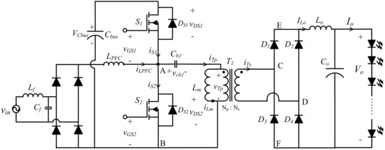
Figure 1.
Proposed dimmable light-emitting diode (LED) driver.
A boost converter performs the function of power-factor correction which consists of an inductor LPFC and the lower arm switch S2. By operating the boost converter in discontinuous-conduction mode (DCM), the peak value of the inductor current iLPFC will follow the track of the rectified input voltage vin. The frequency of iLPFC is far greater than the input-line frequency. The inductor Lf and the capacitor Cf form a low-pass filter which is used to filter out the high frequency component of iLPFC. In this way, the input current can be close to a sinusoidal waveform and in phase with the input-line voltage, thus achieving a high power factor. The magnetizing current in Lm can be used to remove the energy accumulated on parasitic capacitors of S1 and S2 to attain ZVS operation. Thus, the switching losses can be drastically reduced, and the operating efficiency can be promoted.
2.2. Operation Analysis
For simplifying the operation analysis, the following assumptions are made.
- Ignoring the conduction voltage drop for all switching devices, such as diodes and active switches.
- The switching frequency is much greater than the input-line frequency.
- Ignoring voltage ripples on all capacitors because the Cbus and Cb1 are large enough.
- The output inductor Lo is large enough, and its current is assumed to be a constant ILo.
At steady state, the operation of the proposed circuit can be divided into seven modes according to the conducting status of the semiconductor devices in one high-frequency switching cycle. These operation modes and the theoretical voltage and current waveforms of the key components are shown in Figure 2 and Figure 3, respectively. For simplifying the circuit analysis, the low-pass filter and the diode rectifier at the input side are represented by the rectified voltage vrec, and the LED string is represented by its equivalent resistance RLED. The detailed description of each operation mode is as follows.
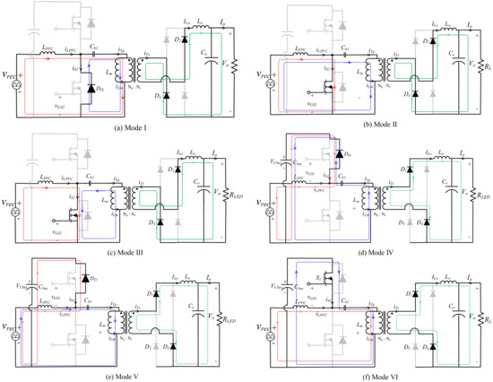
Figure 2.
Operation modes. (a) Mode I, (b) Mode II, (c) Mode III, (d) Mode VI, (e) Mode V, (f) Mode VI, (g) Mode VII.
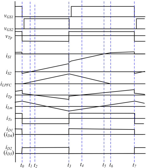
Figure 3.
The theoretic waveforms of key components.
A. Mode I (t0 < t < t1)
As illustrated in Figure 2a, Mode I begins at the time when the gate signal vGS1 turns from a high level to a low level. For maintaining the magnetic flux in Lm, the magnetizing current iLm flows via the capacitor Cb1 and the parasitic capacitance of S2. The parasitic capacitance of S2 is discharged, and the voltage across S2 decreases. Generally, the parasitic capacitance of the active switch is quite small, and it is completely discharged very rapidly. When the energy on the parasitic capacitance of S2 is totally released, iLm diverts from the parasitic capacitance to the intrinsic diode DS2. Hereafter, the voltage across S2, vDS2 is clamped at zero volts. Thus, the ZVS operation can be achieved. The voltage across the primary winding is equal to −VCb1, and diodes D2 and D3 are on, and the current in the secondary winding iTs flows through D2, D3 and Lo. During this interval, iTs is equal to the output inductor current ILo. The iLm and the primary current iTp can be written as Equations (1) and (2), respectively.
where NS and NP represent the turns of the primary winding and the secondary winding, respectively.
Since S2 is clamped at zero volts, the voltage across the PFC inductor is equal to the rectified input voltage. The PFC current increases linearly and is expressed as:
where Vm and fL represent the amplitude and frequency of the input line voltage, respectively. After a very short deadtime, the gate signal vGS2 turns from a low level to a high level in this mode. Based on Equations (1)–(3), iTp decreases. On the contrary, iLPFC increases. The mode ends at the time when iLPFC becomes higher than iTp.
B. Mode II (t1 < t < t2)
The current iS2 is the difference between iLPFC and iTp. Hence, iS2 changes its polarity when iLPFC becomes higher than iTp and S2 is turned on at zero voltage. During this mode, the current equations are the same as Equations (1)–(3). Current iLPFC keeps increasing while iTp keeps decreasing. When iTp decreases to zero, the circuit operation enters Mode III.
C. Mode III (t2 < t < t3)
The current iTp becomes negative at the beginning of this mode. Both iTp and iLPFC flow through S2. The current iLPFC keeps increasing while the current iTp keeps decreasing. As soon as the gate signal vGS2 turns from a high level to a low level, the circuit operation enters Mode IV.
D. Mode IV (t3 < t < t4)
Both the current iLPFC and iTp divert from S2 to flow through the parasitic capacitance of S1 when S2 is turned off. The parasitic capacitance of S1 is discharged, and the voltage across S1, vDS1 decreases. Since the parasitic capacitance is quite small, it is completely discharged very rapidly. When energy on the parasitic capacitance of S1 is totally released, iLPFC and iTp divert from the parasitic capacitance to flow through the intrinsic diode DS1. The voltage across S1, vDS1 is clamped at zero volts. Thus, the ZVS operation can be achieved. During this mode, the voltage across LPFC and the transformer primary winding can be respectively expressed as
The current iLPFC can be expressed as
Regarding a boost-type PFC converter, the dc-link voltage should be designed to be higher than the rectified voltage; therefore, the inductor current iLPFC starts to decrease. The magnetizing current iLm and the primary current can be expressed as
Since the primary voltage is positive, both iLm and iTp increase. On the other hand, the voltage across the secondary winding is positive. Therefore, the secondary winding supplies current to flow through D1 and D4 to the output inductor. After a very short deadtime, the gate signal vGS1 turns from a low level to a high level. This mode ends when iTp becomes zero and changes polarity.
E. Mode V (t4 < t < t5)
In this mode, iTp is smaller than iLPFC. The current flowing through DS1 is equal to iLPFC minus iTp. When iTp becomes higher than iLPFC, S1 is turned on at zero volts, and the circuit enters Mode VI.
F. Mode VI (t5 < t < t6)
In Figure 2f, vGS1 remains at high level and iLPFC keeps decreasing. When iLPFC decreases to zero, the circuit enters Mode VII.
G. Mode VII (t6 < t < t7)
In Figure 2g, the trigger signal vGS1 remains at a high state. The dc-link capacitor Cbus keeps supplying energy via the transformer to the output. At the instant when vGS1 turns into a low state, this mode ends and the circuit operation enters Mode I of the next high-frequency cycle.
3. Circuit Parameter Design
A. Transformer turn ratio n
To simplify the analysis, the voltage across the primary windings of the transformer is idealized as a square-wave voltage source with the amplitude swinging between VCbus–VCb1 and −VCb1, as shown in Figure 4. With the turn ratio of the primary winding to the secondary winding being n:1, the peak-to-peak value across the transformer secondary winding is VCbus/n. Referring to Figure 4, it is known that the average value of the voltage across the primary winding is zero.
where D and T are the duty ratio and the switching period of the active switch S2. From (9), the following can be obtained:
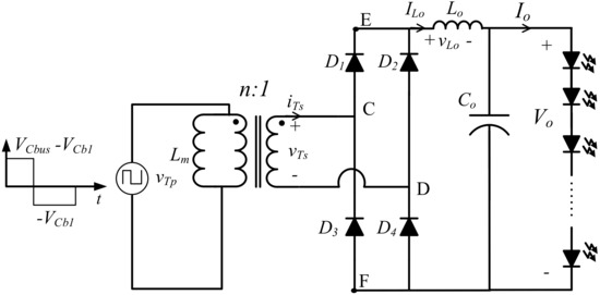
Figure 4.
The simplified circuit of the proposed asymmetrical half-bridge converter.
At steady-state operation, the average voltage of the inductor is zero, i.e., the average value of the rectified voltage of the secondary winding is equal to the output voltage.
Substituting Equation (10) into Equation (11), the transformer turn ratio can be expressed as
B. Output inductor Lo
The selection of the output filter inductance Lo is related to its current ripple. During the conducting interval of S2, the current variation of Lo can be expressed as
By rearranging Equation (13), the inductance of the output inductor can be expressed as:
C. PFC Inductor LPFC
In order to pursue the high power factor, the boost-type PFC converter should be operated at DCM. The inductance of the PFC inductor is inversely proportional to the output power and can be expressed as follows [21].
where Po is the output power; fs is the switching frequency; η is the circuit energy-conversion efficiency, and y is expressed as Equation (16).
4. Illustrative Example and Experimental Results
A prototype of the proposed asymmetrical half-bridge dimmable LED driver was implemented and tested. The driven load is specified as 115 W (96 V/1.2 A), and the associated circuit specification is listed in Table 1. The parameter design, including the transformer turn ratio, the PFC inductor, and the output inductor, is based on the derivation in Section 3. The input filter inductor Lf and input filter capacitor Cf are selected with reference to [22]. By assigning the voltage ripple to be less than 5%, the value of the dc-link capacitor Cbus is obtained with reference to [23]. The component parameters of the practical implementation are listed in Table 2.

Table 1.
Circuit Specification.
Table 2.
Component parameters.
Figure 5 shows the dimming control circuit that mainly consists of a pulse-width-modulation controller (TL494) and a half-bridge driver (IR2302). The TL494 outputs a square-wave voltage of which the oscillation frequency is determined by the capacitor (C2) connected to pin 5 and the resistor connected to pin 5 (R2), and the pulse width is determined by the voltage at pin 4. The output of TL494 is connected to pin 2 of the IR2320. The IR2320 features a high-pulse current buffer stage designed for minimum driver cross-conduction. It outputs two complementary square-wave voltages (HO and LO) used to drive the high and low side MOSFETs (S1 and S2), respectively. The high-side gate driver (HO) is in phase with the logic input (pin 2). Therefore, by varying the resistor R1 to adjust the pulse width of the TL494 output (E1), ASPWM control is achieved with respect to dimming the LEDs.
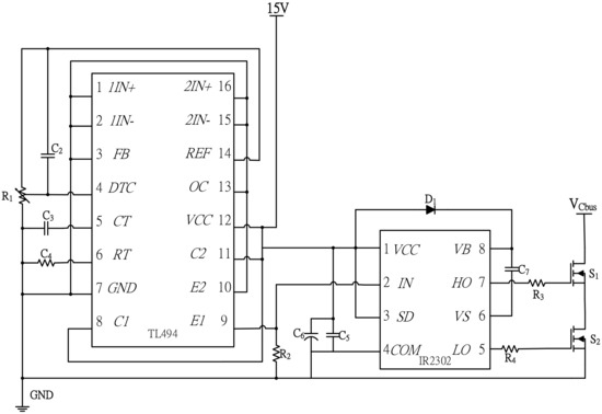
Figure 5.
Control circuit.
Figure 6 shows the measured voltages of the active switches vGS1, vGS2, vDS1, vDS2. It is obvious that prior to the instant when the gate voltages reach a high level, the voltages across the power switches reach nearly zero. This ensures ZVS operation of the active switches. Figure 7 shows the measured diode currents. As expected, these waveforms are consistent with the theoretical ones.
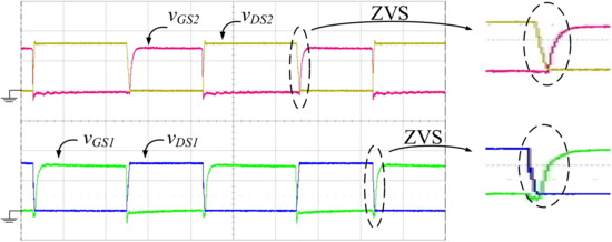
Figure 6.
Voltage waveforms of active switches. (vGS1 and vGS2: 10V/div, vDS1 and vDS2: 200 V/div, Time: 5 μs/div).
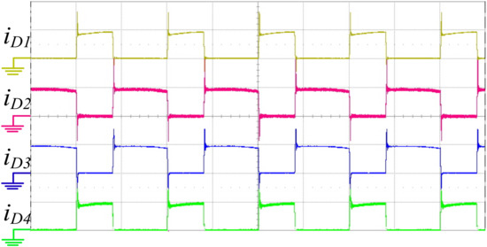
Figure 7.
Current waveforms of rectifying diodes. (iD1, iD2, iD3, iD4: 1 A/div, Time: 10 μs /div).
The LEDs are dimmed from 100% to 4% rated power. Figure 8 shows the waveforms of the gate voltage of S2, the transformer secondary winding current, and the output filter inductor current at different output powers. It can be seen that the LED power is controlled by varying the duty ratio of S2. From (15), for a given PFC inductor, the output power is proportional to the square of the duty ratio. As seen in Figure 7 and Figure 8, there are negative and positive spike currents in the transformer secondary winding and the diodes on its secondary side. In addition, the negative and positive spike currents happen simultaneously. The spike current is the reverse recovery current of the diode. It is seen that the negative spike current happens when a pair of diodes are turned off, and this spike current flows through the transformer secondary winding and the other pair of diodes. Therefore, the positive spike current can be seen in the secondary winding and the other pair of diodes. Figure 9 shows the measured waveforms of the input voltage and PFC inductor current under heavy and light loads. Regardless of a heavy or light load, the peak values of PFC inductor currents always follow the track of the input voltage. Also, the PFC inductor is energized and de-energized at a very high frequency which is hundreds of multiples higher than the input-line frequency. Additionally, the PFC inductor currents coincide well with the input voltage at zero-crossing points, thus warranting the active power-factor correction of the proposed circuit. The measured power factor at different output powers is illustrated in Figure 10. At rated output power (Po = 115 W), the power factor is as high as 0.99. The power factor decreases as the output power decreases the power factor decreases to about 0.92 at 4% rated power. Figure 11 shows the harmonic spectrum of the input line current at the rated power operation. It can be seen that all harmonics are in compliance with the IEC 61000-3-2 Class C standard. The measured THDi is 12.64%. Figure 12 shows the prototype of the proposed LED driver.
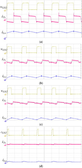
Figure 8.
Waveforms of vGS2, iTs, and iLo at (a) 100%, (b) 50%, (c) 25%, and (d) 4% rated power. (vGS2: 10 V/div, iTs: 2 A/div, iLo: 1 A/div, Time: 10 μs/div).
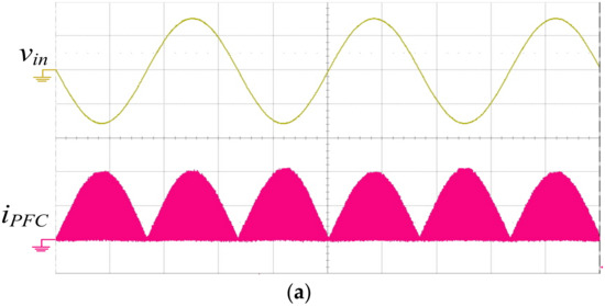
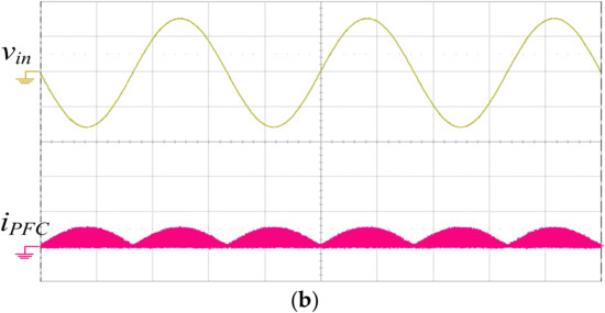
Figure 9.
Waveforms of the input voltage and PFC inductor current. (a) 100% and (b) 4% rated power. (vin: 100 V/div, iPFC: 1 A/div, Time: 5 ms/div).
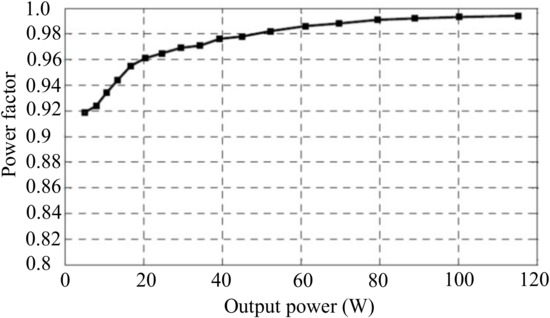
Figure 10.
Power factor versus output power.
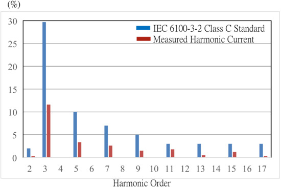
Figure 11.
Harmonic spectrum of the input line current.
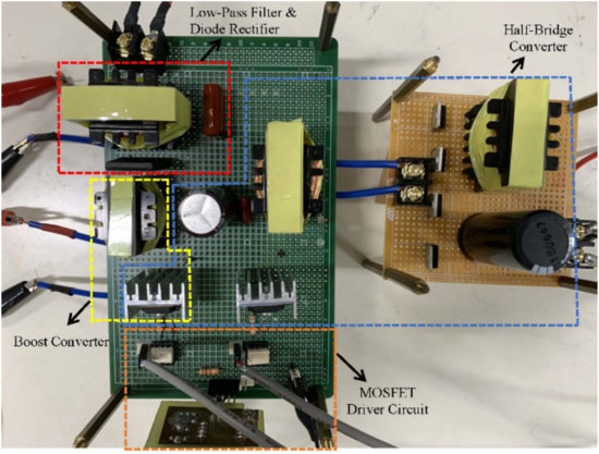
Figure 12.
Prototype LED driver.
5. Conclusions
This study developed and designed a single-stage dimmable LED driver. The circuit topology is derived by integrating a boost converter and an asymmetrical half-bridge converter. The lower-arm switch of the half-bridge converter is shared with the boost converter. The boost converter plays the role of the PFC converter. It operates at DCM to ensure a high power factor at the input line. By freewheeling the PFC inductor and the magnetizing current of the transformer to discharge the parasitic capacitance of the active switches, both active switches can be operated at ZVS, leading to high circuit efficiency. The measured circuit efficiency at rated output power is 92.7%. Experiments are performed to validate the effectiveness of the proposed circuit. The LEDs are dimmed by varying the duty ratio of the active switch. A high power factor is ensured when the LEDs are dimmed from 100% to 4% rated power.
Author Contributions
H.-L.C. and Y.-N.C. conceived and designed the circuit; L.-C.H. and H.-C.Y. performed circuit simulations and designed the parameters of the circuit components; W.-F.Y. carried out the prototype LED driver and measured as well as analyzed the experimental results; H.-L.C. wrote the paper, and S.-Y.C. revised it for submission. All authors have read and agreed to the published version of the manuscript.
Funding
This work was supported by the Ministry of Science and Technology, R.O.C. under the grant MOST 108-2221-E-150-017.
Conflicts of Interest
The authors declare no conflict of interest.
References
- Alonso, J.M.; Perdigão, M.S.; Abdelmessih, G.Z.; Dalla Costa, M.A.; Wang, Y. SPICE modeling of variable inductors and its application to single inductor LED driver design. IEEE Trans. Ind. Electron. 2017, 64, 5894–5903. [Google Scholar] [CrossRef]
- Rodgaard, M.S.; Weirich, M.; Andersen, M.A.E. Forward conduction mode controlled piezoelectric transformer based PFC LED driver. IEEE Trans. Power Electron. 2013, 28, 4841–4849. [Google Scholar] [CrossRef]
- Li, Y.C.; Chen, C.L. A novel primary-side regulation scheme for single-stage high-power-factor AC-DC LED driving circuit. IEEE Trans. Ind. Electron. 2013, 60, 4978–4986. [Google Scholar] [CrossRef]
- Lee, S.W.; Choe, H.J.; Yun, J.J. Performance improvement of a boost LED driver with high voltage gain for edge-lit LED backlights. IEEE Trans. Circuits Syst. II 2018, 65, 481–485. [Google Scholar] [CrossRef]
- Luo, Q.; Huang, J.; He, Q.; Ma, K.; Zhou, L. Analysis and design of a single-stage isolated AC-DC LED driver with a voltage doubler rectifier. IEEE Trans. Ind. Electron. 2017, 64, 5807–5817. [Google Scholar] [CrossRef]
- Wang, C.M.; Lin, C.H.; Yang, T.C. High-power-factor soft-switched dc power supply system. IEEE Trans. Power Electron. 2011, 26, 647–654. [Google Scholar] [CrossRef]
- Mousavi, A.; Das, P.; Moschopoulos, G. A comparative study of a new ZCS DC-DC full-bridge boost converter with a ZVS active-Clamp converter. IEEE Trans. Power Electron. 2012, 27, 1347–1358. [Google Scholar] [CrossRef]
- Liu, Y.C.; Huang, B.S.; Lin, C.H.; Kim, K.A.; Chiu, H.J. Design and implementation of a high power density active-clamped flyback converter. In Proceedings of the 2018 International Power Electronics Conference, Niigata, Japan, 20–24 May 2018; pp. 2092–2096. [Google Scholar]
- Bhatt, K.; Gupta, R.A.; Gupta, N. Average model of isolated bidirectional dc-dc converter with auxiliary isolated clamp. In Proceedings of the 8th IEEE India International Conference on Power Electronics, Jaipur, India, 13–15 December 2018; pp. 1–5. [Google Scholar]
- Alonso, J.M.; Viña, J.; Vaquero, D.G.; Martínez, G.; Osório, R. Analysis and design of the integrated double buck-boost converter as a high-power-factor driver for power-LED lamps. IEEE Trans. Ind. Electron. 2012, 59, 1689–1697. [Google Scholar] [CrossRef]
- Wang, Y.; Guan, Y.; Ren, K.; Wang, W.; Xu, D. A single-stage LED driver based on BCM boost circuit and LLC converter for street lighting system. IEEE Trans. Ind. Electron. 2015, 62, 5446–5457. [Google Scholar] [CrossRef]
- Chen, S.Y.; Li, Z.R.; Chen, C.L. Analysis and design of single-stage ac/dc LLC resonant converter. IEEE Trans. Ind. Electron. 2012, 59, 1538–1544. [Google Scholar] [CrossRef]
- Cheng, C.A.; Chang, C.H.; Chun, T.Y.; Yang, F.L. Design and implementation of a single-stage driver for supplying an LED street-lighting module with power factor corrections. IEEE Trans. Power Electron. 2015, 30, 956–966. [Google Scholar] [CrossRef]
- Wang, Y.; Alonso, J.M.; Ruan, X. A review of LED drivers and related technologies. IEEE Trans. Ind. Electron. 2017, 64, 5754–5765. [Google Scholar] [CrossRef]
- Ma, J.; Wei, X.; Hu, L.; Zhang, J. LED driver based on boost circuit and LLC converter. IEEE Access. 2018, 6, 49588–49600. [Google Scholar] [CrossRef]
- Singh, S.; Singh, B. A voltage controlled adjustable speed PMBLDCM drive using a single-stage PFC half-bridge converter. In Proceedings of the IEEE APEC 2010, Palm Springs, CA, USA, 21–25 February 2010; pp. 1976–1983. [Google Scholar]
- Ou, S.; Hsiao, H. Analysis and design of a novel single-stage switching power supply with half-bridge topology. IEEE Trans. Power Electron. 2011, 26, 3230–3241. [Google Scholar] [CrossRef]
- Taheri, M.; Milimonfared, J.; Bayat, H.; Fathi, S.H. Analysis, design and implementation of a new zero-voltage-switching interleaved asymmetrical half-bridge converter using an integrated transformer. IET Power Electron. 2012, 1912–1922. [Google Scholar] [CrossRef]
- Choi, W.-Y.; Yoo, J.-S. A bridgeless single-stage half-bridge AC/DC converter. IEEE Trans. Power Electron. 2011, 26, 3884–3895. [Google Scholar] [CrossRef]
- Muhlethaler, J.; Biela, J.; Kolar, J.W.; Ecklebe, A. Core losses under the DC bias condition based on Steinmetz parameters. IEEE Trans. Power Electron. 2012, 27, 953–963. [Google Scholar] [CrossRef]
- Liang, T.J.; Kang, S.C.; Cheng, C.A.; Lin, R.L.; Chen, J.F. Analysis and design of single-stage electronic ballast with bridgeless PFC configuration. In Proceedings of the 29th Annual Conference on IEEE Industrial Electronics Society (IECON 2003), Roanoke, VA, USA, 2–6 November 2003; pp. 502–508. [Google Scholar]
- Moo, C.S.; Yen, H.C.; Hsieh, Y.C.; Chuang, Y.C. Integrated design of EMI filter and PFC low-pass filter for power electronic converters. Proc. Inst. Elect. Eng. Elect. Power Appl. 2003, 150, 39–44. [Google Scholar] [CrossRef]
- Chang, Y.N. Self-excited single-stage power factor correction driving circuit for LED lighting. Hindawi Publ. Corp. J. Nanomater. 2014, 2014. [Google Scholar] [CrossRef]
© 2020 by the authors. Licensee MDPI, Basel, Switzerland. This article is an open access article distributed under the terms and conditions of the Creative Commons Attribution (CC BY) license (http://creativecommons.org/licenses/by/4.0/).