Atomic Layer Deposition of High-k Insulators on Epitaxial Graphene: A Review

 ,
, 
 and
and
Abstract
Featured Application
Abstract
1. Introduction
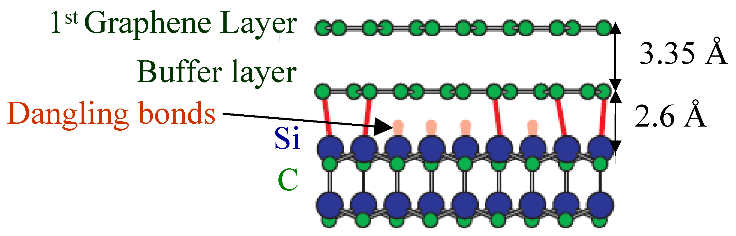
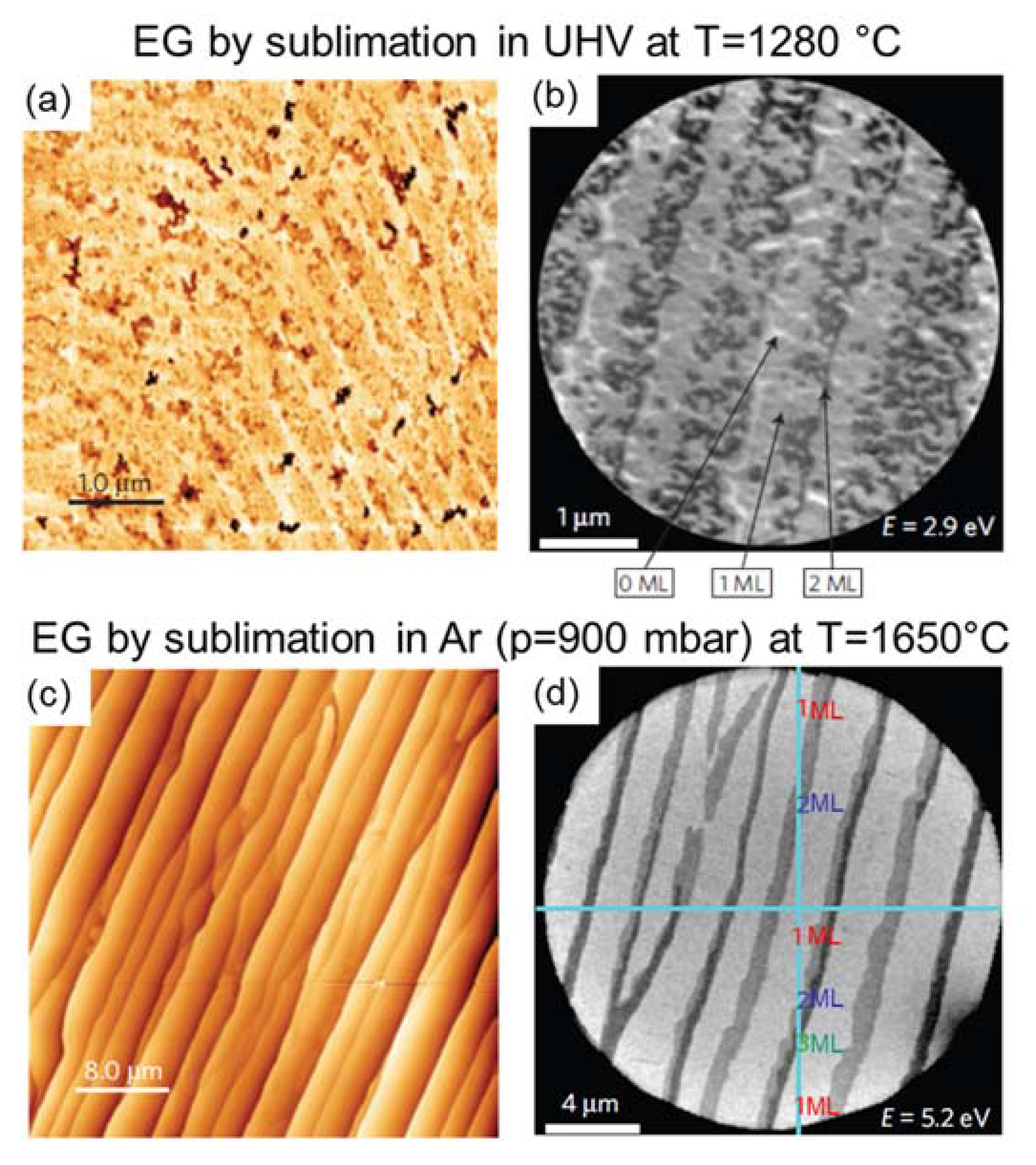
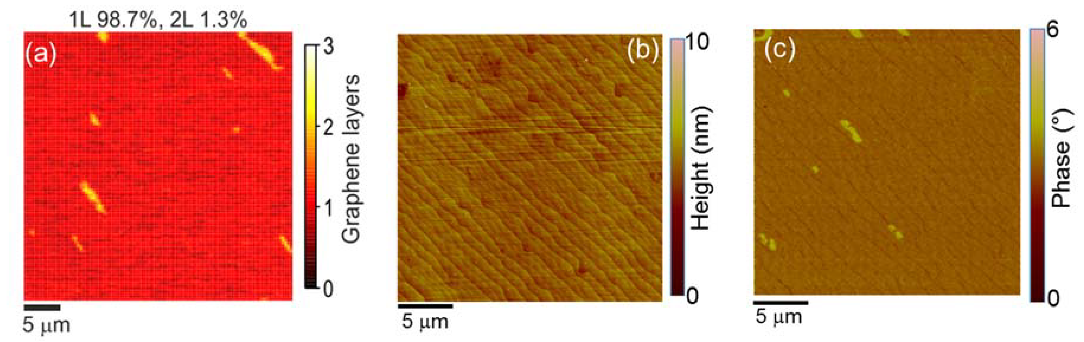
2. Morphology and Interface Structure of Epitaxial Graphene on SiC (0001)
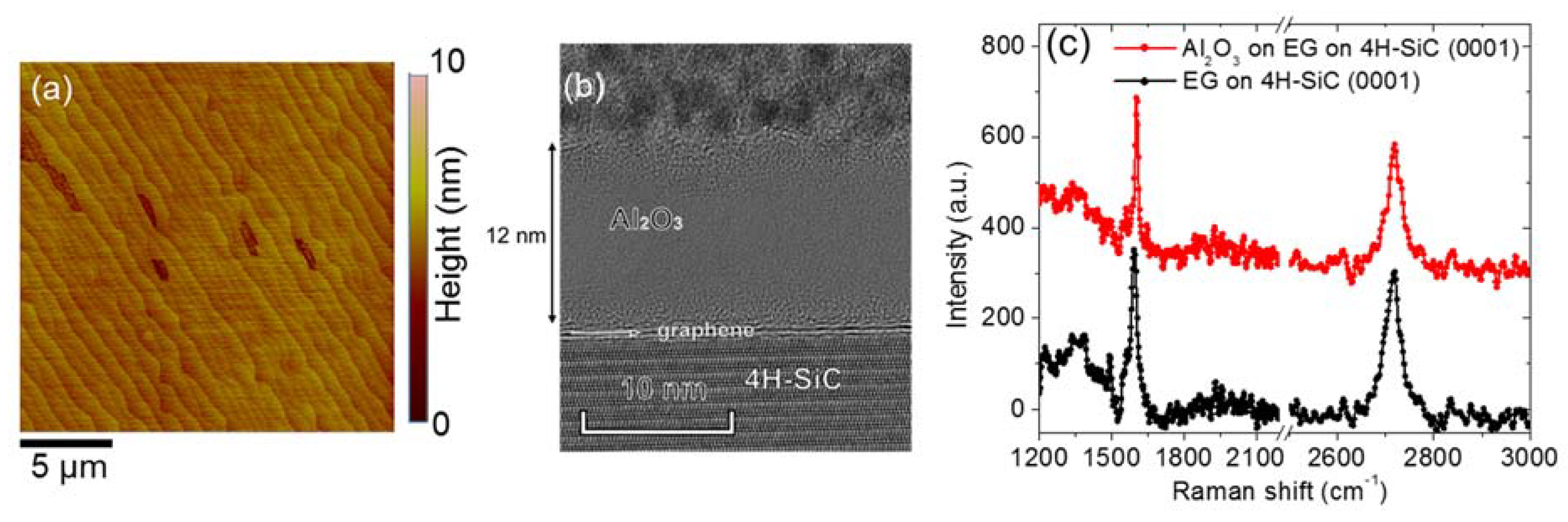
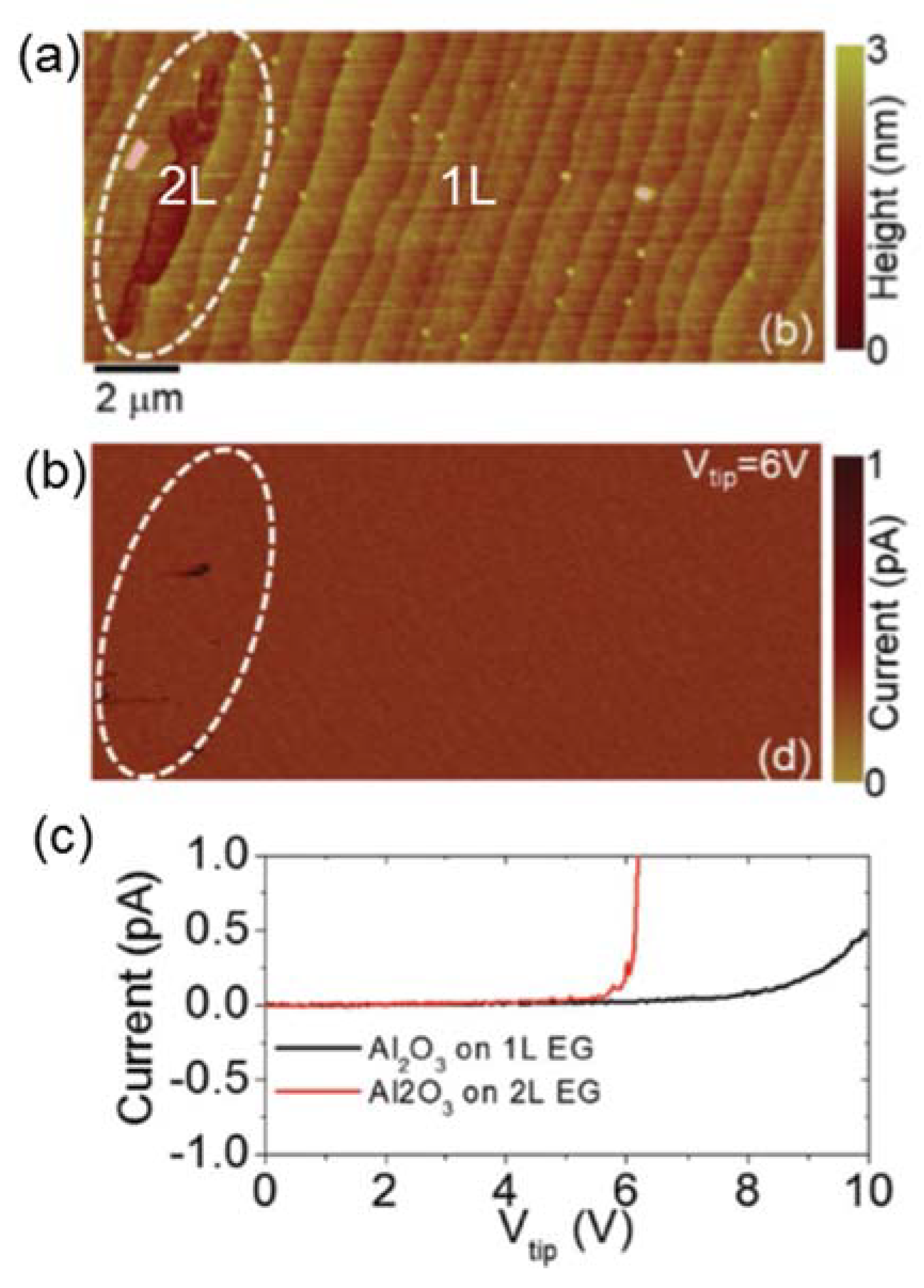
3. Direct ALD on Pristine Epitaxial Graphene
4. ALD on EG With a Seeding-Layer
4.1. Oxidized Metal Seed Layer
4.2. Deposited High-k Metal-Oxide Seed Layers
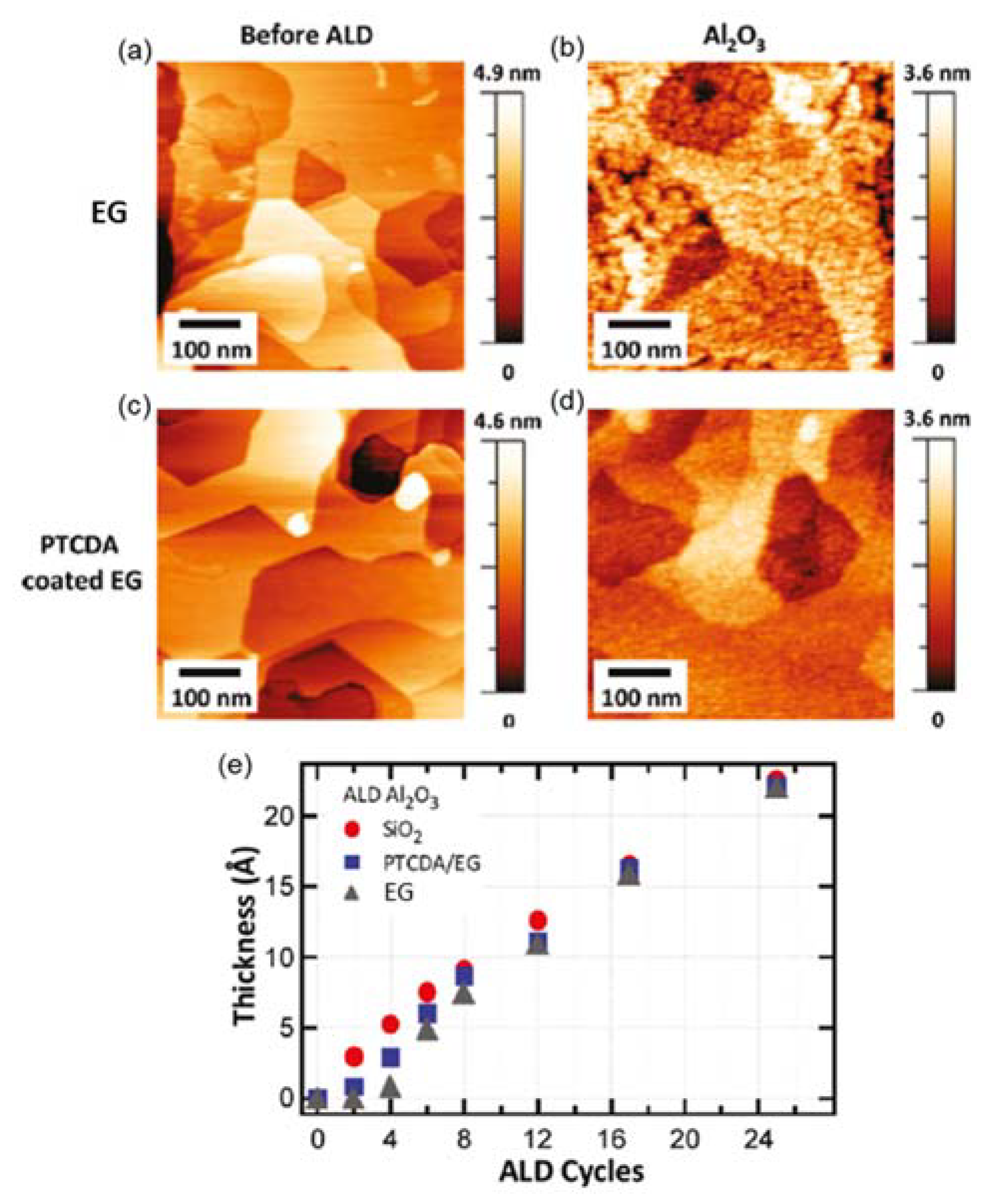
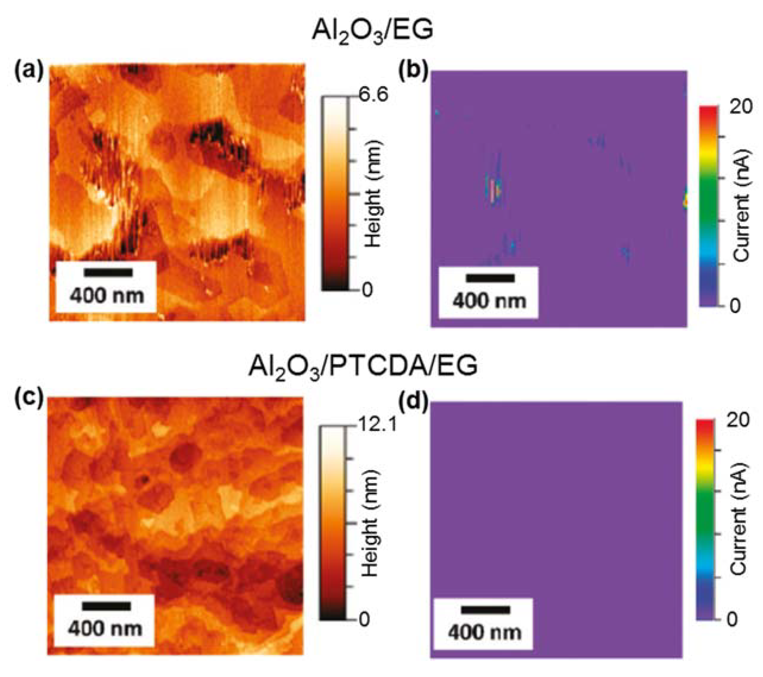
4.3. Self-Assembled Organic Monolayer
5. ALD on Prefunctionalized EG
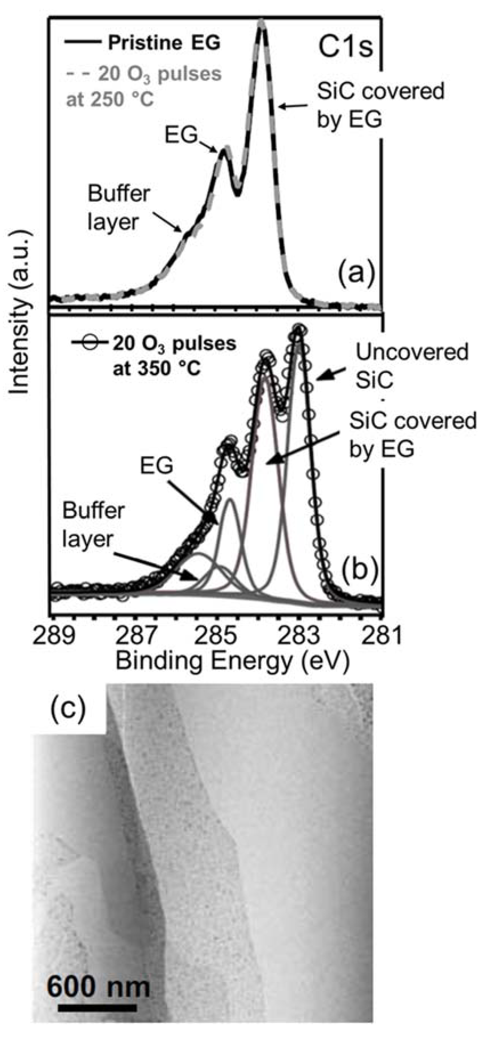
5.1. Ozone Prefunctionalization
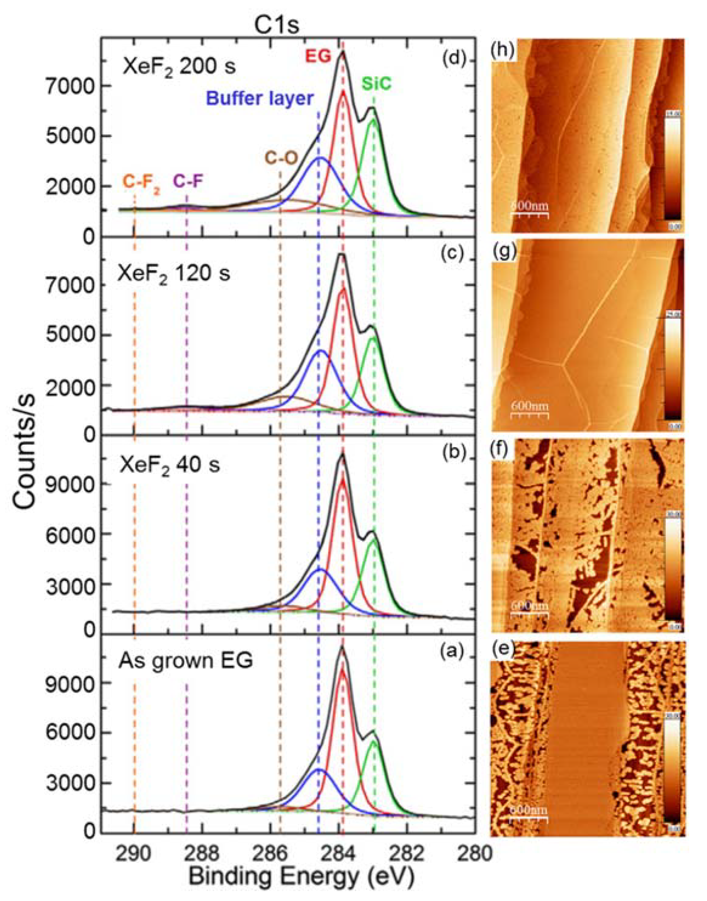
5.2. Fluorine Prefunctionalization
6. Open Research Issues and Perspectives
7. Conclusions
Author Contributions
Funding
Acknowledgments
Conflicts of Interest
References
- Novoselov, K.S.; Geim, A.K.; Morozov, S.V.; Jiang, D.; Zhang, Y.; Dubonos, S.V.; Grigorieva, I.V.; Firsov, A.A. Electric Field Effect in Atomically Thin Carbon Films. Science 2004, 306, 666–669. [Google Scholar] [CrossRef] [PubMed]
- Berger, C.; Song, Z.; Li, X.; Wu, X.; Brown, N.; Naud, C.; Mayou, D.; Li, T.; Hass, J.; Marchenkov, A.N.; et al. Electronic confinement and coherence in patterned epitaxial graphene. Science 2006, 312, 1191–1196. [Google Scholar] [CrossRef] [PubMed]
- Emtsev, K.V.; Bostwick, A.; Horn, K.; Jobst, J.; Kellogg, G.L.; Ley, L.; McChesney, J.L.; Ohta, T.; Reshanov, S.A.; Rohrl, J.; et al. Towards wafer-size graphene layers by atmospheric pressure graphitization of SiC(0001). Nat. Mater. 2009, 8, 203–207. [Google Scholar] [CrossRef] [PubMed]
- Virojanadara, C.; Syvajarvi, M.; Yakimova, R.; Johansson, L.I.; Zakharov, A.A.; Balasubramanian, T. Homogeneous large-area graphene layer growth on 6H-SiC(0001). Phys. Rev. B 2008, 78, 245403. [Google Scholar] [CrossRef]
- Moon, J.S.; Curtis, D.; Hu, M.; Wong, D.; McGuire, C.; Campbell, P.M.; Jernigan, G.; Tedesco, J.L.; VanMil, B.; Myers-Ward, R.; et al. Epitaxial-Graphene RF Field-Effect Transistors on Si-Face 6H-SiC Substrates. IEEE Electron Device Lett. 2009, 30, 650–652. [Google Scholar] [CrossRef]
- Lin, Y.-M.; Dimitrakopoulos, C.; Jenkins, K.A.; Farmer, D.B.; Chiu, H.-Y.; Grill, A.; Avouris, P. 100-GHz Transistors from Wafer-Scale Epitaxial Graphene. Science 2010, 327, 662. [Google Scholar] [CrossRef]
- Tzalenchuk, A.; Lara-Avila, S.; Kalaboukhov, A.; Paolillo, S.; Syväjärvi, M.; Yakimova, R.; Kazakova, O.; Janssen, T.J.B.M.; Fal’ko, V.; Kubatkin, S. Towards a quantum resistance standard based on epitaxial graphene. Nat. Nanotechnol. 2010, 5, 186–189. [Google Scholar] [CrossRef]
- Pearce, R.; Iakimov, T.; Andersson, M.; Hultman, L.; Lloyd Spetz, A.; Yakimova, R. Epitaxially grown graphene based gas sensors for ultra sensitive NO2 detection. Sens. Actuators B 2011, 155, 451–455. [Google Scholar] [CrossRef]
- Li, X.; Cai, W.; An, J.; Kim, S.; Nah, J.; Yang, D.; Piner, R.; Velamakanni, A.; Jung, I.; Tutuc, E.; et al. Large-area synthesis of high-quality and uniform graphene films on copper foils. Science 2009, 324, 1312–1314. [Google Scholar] [CrossRef]
- Kang, J.; Shin, D.; Bae, S.; Hong, B.H. Graphene transfer: Key for applications. Nanoscale 2012, 4, 5527. [Google Scholar] [CrossRef]
- Fisichella, G.; Di Franco, S.; Roccaforte, F.; Ravesi, S.; Giannazzo, F. Microscopic mechanisms of graphene electrolytic delamination from metal substrates. Appl. Phys. Lett. 2014, 104, 233105. [Google Scholar] [CrossRef]
- Lin, Y.; Lu, C.; Yeh, C.; Jin, C.; Suenaga, K.; Chiu, P. Graphene Annealing: How Clean Can It Be? Nano Lett. 2012, 12, 414–419. [Google Scholar] [CrossRef] [PubMed]
- Lupina, G.; Kitzmann, J.; Costina, I.; Lukosius, M.; Wenger, C.; Wolff, A.; Vaziri, S.; Ostling, M.; Pasternak, I.; Krajewska, A.; et al. Residual metallic contamination of transferred chemical vapor deposited graphene. ACS Nano 2015, 9, 4776. [Google Scholar] [CrossRef] [PubMed]
- Wu, Y.; Lin, Y.; Bol, A.A.; Jenkins, K.A.; Xia, F.; Farmer, D.B.; Zhu, Y.; Avouris, P. High-Frequency, Scaled Graphene Transistors on Diamond-Like Carbon. Nature 2011, 472, 74–78. [Google Scholar] [CrossRef] [PubMed]
- Mehr, W.; Dabrowski, J.; Scheytt, J.C.; Lippert, G.; Xie, Y.H.; Lemme, M.C.; Ostling, M.; Lupina, G. Vertical Graphene Base Transistor. IEEE Electron Device Lett. 2012, 33, 691–693. [Google Scholar] [CrossRef]
- Giannazzo, F.; Greco, G.; Roccaforte, F.; Sonde, S.S. Vertical Transistors Based on 2D Materials: Status and Prospects. Crystals 2018, 8, 70. [Google Scholar] [CrossRef]
- Giannazzo, F.; Greco, G.; Schilirò, E.; Lo Nigro, R.; Deretzis, I.; La Magna, A.; Roccaforte, F.; Iucolano, F.; Ravesi, S.; Frayssinet, E.; et al. High-Performance Graphene/AlGaN/GaN Schottky Junctions for Hot Electron Transistors. ACS Appl. Electron. Mater. 2019, 1, 2342–2354. [Google Scholar] [CrossRef]
- Pakalla, A.; Putkonen, M. Handbook of Deposition Technologies for Films and Coatings, 3rd ed.; Elsevier: Amsterdam, The Netherlands, 2010; pp. 364–391. [Google Scholar]
- Wang, X.; Tabakman, S.M.; Dai, H. Atomic Layer Deposition of Metal Oxides on Pristine and Functionalized Graphene. J. Am. Chem. Soc. 2008, 130, 8152. [Google Scholar] [CrossRef]
- Vervuurt, R.H.J.; Karasulu, B.; Verheijen, M.A.; Kessels, W.M.M.; Bol, A.A. Uniform Atomic Layer Deposition of Al2O3 on Graphene by Reversible Hydrogen Plasma Functionalization. Chem. Mater. 2017, 29, 2090. [Google Scholar] [CrossRef]
- Schilirò, E.; Lo Nigro, R.; Roccaforte, F.; Deretzis, J.; La Magna, A.; Armano, A.; Agnello, S.; Pecz, B.; Ivanov, I.G.; Giannazzo, F. Seed-Layer-Free Atomic Layer Deposition of Highly Uniform Al2O3 Thin Films onto Monolayer Epitaxial Graphene on Silicon Carbide. Adv. Mater. Interfaces 2019, 6, 1900097. [Google Scholar] [CrossRef]
- Lin, Y.-M.; Jenkins, K.A.; Valdes-Garcia, A.; Small, J.P.; Farmer, D.B.; Avouris, P. Operation of Graphene Transistors at Gigahertz Frequencies. Nano Lett. 2008, 9, 422. [Google Scholar] [CrossRef]
- Kim, S.; Nah, J.; Jo, I.; Shahrjerdi, D.; Colombo, L.; Yao, Z.; Tutuc, E.; Banerjee, S.K. Realization of a high mobility dual-gated graphene field-effect transistor with Al2O3 dielectric. Appl. Phys. Lett. 2009, 94, 062107. [Google Scholar] [CrossRef]
- Fisichella, G.; Schilirò, E.; Di Franco, S.; Fiorenza, P.; Lo Nigro, R.; Roccaforte, F.; Ravesi, S.; Giannazzo, F. Interface Electrical Properties of Al2O3 Thin Films on Graphene Obtained by Atomic Layer Deposition with an in Situ Seedlike Layer. ACS Appl. Mater. Interfaces 2017, 9, 7761–7771. [Google Scholar] [CrossRef] [PubMed]
- Shen, T.; Gu, J.J.; Xu, M.; Wu, Y.Q.; Bolen, M.L.; Capano, M.A.; Engel, L.W.; Ye, P.D. Observation of quantum-Hall effect in gated epitaxial graphene grown on SiC (0001). Appl. Phys. Lett. 2009, 95, 172105. [Google Scholar] [CrossRef]
- Fallahazad, B.; Lee, K.; Lian, G.; Kim, S.; Corbet, C.M.; Ferrer, D.A.; Colombo, L.; Tutuc, E. Scaling of Al2O3 dielectric for graphene field-effect transistors. Appl. Phys. Lett. 2012, 100, 093112. [Google Scholar] [CrossRef]
- Meric, I.; Dean, C.R.; Young, A.F.; Baklitskaya, N.; Tremblay, N.J.; Nuckolls, C.; Kim, P.; Shepard, K.L. Channel length scaling in graphene field-effect transistors studied with pulsed current-voltage measurements. Nano Lett. 2011, 11, 1093. [Google Scholar] [CrossRef] [PubMed]
- Farmer, D.B.; Chiu, H.-Y.; Lin, Y.-M.; Jenkins, K.A.; Xia, F.; Avouris, P. Utilization of a Buffered Dielectric to Achieve High Field-Effect Carrier Mobility in Graphene Transistors. Nano Lett. 2009, 9, 4474. [Google Scholar] [CrossRef] [PubMed]
- Lim, T.; Kim, D.; Ju, S. Direct deposition of aluminum oxide gate dielectric on graphene channel using nitrogen plasma treatment. Appl. Phys. Lett. 2013, 113, 013107. [Google Scholar] [CrossRef]
- Schilirò, E.; Lo Nigro, R.; Roccaforte, F.; Giannazzo, F. Recent Advances in Seeded and Seed-Layer-Free Atomic Layer Deposition of High-K Dielectrics on Graphene for Electronics. C J. Carbon Res. 2019, 5, 53. [Google Scholar]
- Lee, B.; Mordi, G.; Kim, M.J.; Chabal, Y.J.; Vogel, E.M.; Wallace, R.M.; Cho, K.J.; Colombo, L.; Kim, J. Characteristics of high-k Al2O3 dielectric using ozone-based atomic layer deposition for dual-gated graphene devices. Appl. Phys. Lett. 2010, 97, 043107. [Google Scholar] [CrossRef]
- Lee, B.; Park, S.-Y.; Kim, H.-C.; Cho, K.; Vogel, E.M.; Kim, M.J.; Wallace, R.M.; Kim, J. Conformal Al2O3 dielectric layer deposited by atomic layer deposition for graphene-based nanoelectronics. Appl. Phys. Lett. 2008, 92, 203102. [Google Scholar] [CrossRef]
- Vervuurt, R.H.J.; Kessels, W.M.M.; Bol, A.A. Atomic Layer Deposition for Graphene Device Integration. Adv. Mater. Interfaces 2017, 4, 1700232. [Google Scholar] [CrossRef]
- Robinson, J.A.; LaBella, M.; Trumbull, K.A.; Weng, X.; Cavelero, R.; Daniels, T.; Hughes, Z.; Hollander, M.; Fanton, M.; Snyder, D. Epitaxial Graphene Materials Integration: Effects of Dielectric Overlayers on Structural and Electronic Properties. ACS Nano 2010, 4, 2667–2672. [Google Scholar] [CrossRef] [PubMed]
- Hollander, M.J.; LaBella, M.; Hughes, Z.R.; Zhu, M.; Trumbull, K.A.; Cavalero, R.; Snyder, D.W.; Wang, X.; Hwang, E.; Datta, S.; et al. Enhanced Transport and Transistor Performance with Oxide Seeded High-k Gate Dielectrics on Wafer-Scale Epitaxial Graphene. Nano Lett. 2011, 11, 3601. [Google Scholar] [CrossRef]
- Alaboson, J.M.P.; Wang, Q.H.; Emery, J.D.; Lipson, A.L.; Bedzyk, M.J.; Elam, J.W.; Pellin, M.J.; Hersam, M.C. Seeding Atomic Layer Deposition of High-k Dielectrics on Epitaxial Graphene with Organic Self-Assembled Monolayers. ACS Nano 2011, 5, 5223–5232. [Google Scholar] [CrossRef]
- Nath, A.; Kong, B.D.; Koehler, A.D.; Anderson, V.R.; Wheeler, V.D.; Daniels, K.M.; Boyd, A.K.; Cleveland, E.R.; Myers-Ward, R.L.; Gaskill, D.K.; et al. Universal conformal ultrathin dielectrics on epitaxial graphene enabled by a graphene oxide seed layer. Appl. Phys. Lett. 2017, 110, 013106. [Google Scholar] [CrossRef]
- Speck, F.; Ostler, M.; Röhrl, J.; Emtsev, K.V.; Hundhausen, M.; Ley, L.; Seyller, T. Atomic layer deposited aluminum oxide films on graphite and graphene studied by XPS and AFM. Phys. Status Solidi C 2010, 7, 398–401. [Google Scholar] [CrossRef]
- Wheeler, V.; Garces, N.; Nyakiti, L.; Myers-Ward, R.; Jernigan, G.; Culbertson, J.; Eddy, C., Jr.; Gaskill, D.K. Fluorine functionalization of epitaxial graphene for uniform deposition of thin high-k dielectrics. Carbon 2012, 50, 2307–2314. [Google Scholar] [CrossRef]
- Emtsev, K.V.; Speck, F.; Seyller, T.; Ley, L.; Riley, J.D. Interaction, growth, and ordering of epitaxial graphene on SiC{0001} surfaces: A comparative photoelectron spectroscopy study. Phys. Rev. B 2008, 77, 155303. [Google Scholar] [CrossRef]
- Jabakhanji, B.; Camara, N.; Caboni, A.; Consejo, C.; Jouault, B.; Godignon, P.; Camassel, J. Almost Free Standing Graphene on SiC(000-1) and SiC(11-20). Mater. Sci. Forum 2012, 711, 235–241. [Google Scholar] [CrossRef]
- Bouhafs, C.; Zakharov, A.A.; Ivanov, I.G.; Giannazzo, F.; Eriksson, J.; Stanishev, V.; Kühne, P.; Iakimov, T.; Hofmann, T.; Schubert, M.; et al. Multi-scale investigation of interface properties, stacking order and decoupling of few layer graphene on C-face 4H-SiC. Carbon 2017, 116, 722–732. [Google Scholar] [CrossRef]
- Nicotra, G.; Deretzis, I.; Scuderi, M.; Spinella, C.; Longo, P.; Yakimova, R.; Giannazzo, F.; La Magna, A. Interface disorder probed at the atomic scale for graphene grown on the C face of SiC. Phys. Rev. B 2015, 91, 15541. [Google Scholar] [CrossRef]
- Ostler, M.; Deretzis, I.; Mammadov, S.; Giannazzo, F.; Nicotra, G.; Spinella, C.; Seyller, T.; La Magna, A. Direct growth of quasi-free-standing epitaxial graphene on nonpolar SiC surfaces. Phys. Rev. B 2013, 88, 085408. [Google Scholar] [CrossRef]
- Varchon, F.; Feng, R.; Hass, J.; Li, X.; Ngoc Nguyen, B.; Naud, C.; Mallet, P.; Veuillen, J.-Y.; Berger, C.; Conrad, E.H.; et al. Electronic Structure of Epitaxial Graphene Layers on SiC: Effect of the Substrate. Phys. Rev. Lett. 2007, 99, 126805. [Google Scholar] [CrossRef]
- Riedl, C.; Zakharov, A.A.; Starke, U.; Riedl, C. Precise in situ thickness analysis of epitaxial graphene layers on SiC(0001) using low-energy electron diffraction and angle resolved ultraviolet photoelectron spectroscopy. Appl. Phys. Lett. 2008, 93, 033106. [Google Scholar] [CrossRef]
- Sonde, S.; Giannazzo, F.; Raineri, V.; Yakimova, R.; Huntzinger, J.-R.; Tiberj, A.; Camassel, J. Electrical properties of the graphene/4H-SiC (0001) interface probed by scanning current spectroscopy. J. Phys. Rev. B 2009, 80, 241406. [Google Scholar] [CrossRef]
- Vecchio, C.; Sonde, S.; Bongiorno, C.; Rambach, M.; Yakimova, R.; Rimini, E.; Raineri, V.; Giannazzo, F. Nanoscale structural characterization of epitaxial graphene grown on off-axis 4H-SiC (0001). Nanoscale Res. Lett. 2011, 6, 269. [Google Scholar] [CrossRef]
- Giannazzo, F.; Deretzis, I.; La Magna, A.; Roccaforte, F.; Yakimova, R. Electronic transport at monolayer-bilayer junctions in epitaxial graphene on SiC. Phys. Rev. B 2012, 86, 235422. [Google Scholar] [CrossRef]
- Nicotra, G.; Ramasse, Q.M.; Deretzis, I.; La Magna, A.; Spinella, C.; Giannazzo, F. Delaminated Graphene at Silicon Carbide Facets: Atomic Scale Imaging and Spectroscopy. ACS Nano 2013, 7, 3045–3052. [Google Scholar] [CrossRef]
- Ivanov, I.G.; Ul Hassan, J.; Iakimov, T.; Zakharov, A.A.; Yakimova, R.; Janzén, E. Layer number determination in graphene on SiC by reflectance mapping. Carbon 2014, 77, 492. [Google Scholar] [CrossRef]
- Lee, D.S.; Riedl, C.; Krauss, B.; von Klitzing, K.; Starke, U.; Smet, J.H. Raman Spectra of Epitaxial Graphene on SiC and of Epitaxial Graphene Transferred to SiO2. Nano Lett. 2008, 8, 4320. [Google Scholar] [CrossRef]
- Hong, G.; Han, Y.; Schutzius, T.M.; Wang, Y.; Pan, Y.; Hu, M.; Jie, J.; Sharma, C.S.; Muller, U.; Poulikakos, D. On the Mechanism of Hydrophilicity of Graphene. Nano Lett. 2016, 16, 4447. [Google Scholar] [CrossRef]
- Giannazzo, F.; Sonde, S.; Lo Nigro, R.; Rimini, E.; Raineri, V. Mapping the Density of Scattering Centers Limiting the Electron Mean Free Path in Graphene. Nano Lett. 2011, 11, 4612–4618. [Google Scholar] [CrossRef]
- Touhara, H.; Okino, F. Property control of carbon materials by fluorination. Carbon 2000, 38, 241–267. [Google Scholar] [CrossRef]
- Lemme, M.C.; Echtermeyer, T.J.; Baus, M.; Kurz, H. A Graphene Field-Effect Device. IEEE Electron Device Lett. 2007, 28, 282–284. [Google Scholar] [CrossRef]
- Ni, Z.H.; Wang, H.M.; Ma, Y.; Kasim, J.; Wu, Y.H.; Shen, Z.X. Tunable Stress and Controlled Thickness Modification in Graphene by Annealing. ACS Nano 2008, 2, 1033–1039. [Google Scholar] [CrossRef]
- Dlubak, B.; Kidambi, P.R.; Weatherup, R.S.; Hofmann, S.; Robertson, J. Substrate-assisted nucleation of ultra-thin dielectric layers on graphene by atomic layer deposition. Appl. Phys. Lett. 2012, 100, 173113. [Google Scholar] [CrossRef]
- Rafiee, J.; Mi, X.; Gullapalli, H.; Thomas, A.V.; Yavari, F.; Shi, Y.; Ajayan, P.M.; Koratkar, N.A. Wetting transparency of graphene. Nat. Mater. 2012, 11, 217–222. [Google Scholar] [CrossRef]
- Cabrero-Vilatela, A.; Alexander-Webber, J.A.; Sagade, A.A.; Aria, A.I.; Braeuninger-Weimer, P.; Martin, M.-B.; Weatherup, R.S.; Hofmann, S. Atomic layer deposited oxide films as protective interface layers for integrated graphene transfer. Nanotechnology 2017, 28, 485201. [Google Scholar] [CrossRef]
- Giannazzo, F.; Fisichella, G.; Greco, G.; La Magna, A.; Roccaforte, F.; Pecz, B.; Yakimova, R.; Dagher, R.; Michon, A.; Cordier, Y. Graphene integration with nitride semiconductors for high power and high frequency electronics. Phys. Status Solidi A 2017, 214, 1600460. [Google Scholar] [CrossRef]
- Zubair, A.; Nourbakhsh, A.; Hong, J.-Y.; Qi, M.; Song, Y.; Jena, D.; Kong, J.; Dresselhaus, M.; Palacios, T. Hot Electron Transistor with van der Waals Base-Collector Heterojunction and High- Performance GaN Emitter. Nano Lett. 2017, 17, 3089–3096. [Google Scholar] [CrossRef] [PubMed]
- Meng, X.; Byun, Y.-C.; Kim, H.S.; Lee, J.S.; Lucero, A.T.; Cheng, L.; Kim, J. Atomic Layer Deposition of Silicon Nitride Thin Films: A Review of Recent Progress, Challenges, and Outlooks. Materials 2016, 9, 1007. [Google Scholar] [CrossRef] [PubMed]
- Schilirò, E.; Giannazzo, F.; Bongiorno, C.; Di Franco, S.; Greco, G.; Roccaforte, F.; Prystawko, P.; Kruszewski, P.; Leszczyński, M.; Krysko, M.; et al. Structural and electrical properties of AlN thin films on GaN substrates grown by plasma enhanced-Atomic Layer Deposition. Mater. Sci. Semicond. Process. 2019, 97, 35–39. [Google Scholar] [CrossRef]
- Dean, C.R.; Young, A.F.; Meric, I.; Lee, C.; Wang, L.; Sorgenfrei, S.; Watanabe, K.; Taniguchi, T.; Kim, P.; Shepard, K.L.; et al. Boron nitride substrates for high-quality graphene electronics. Nat. Nanotechnol. 2010, 5, 722. [Google Scholar] [CrossRef]
- Takahashi, N.; Watanabe, K.; Taniguchi, T.; Nagashio, K. Atomic layer deposition of Y2O3 on h-BN for a gate stack in graphene FETs. Nanotechnology 2015, 26, 175708. [Google Scholar] [CrossRef]
- Lin, Y.-C.; Ghosh, R.K.; Addou, R.; Lu, N.; Eichfeld, S.M.; Zhu, H.; Li, M.-Y.; Peng, X.; Kim, M.J.; Li, L.-J.; et al. Atomically thin resonant tunnel diodes built from synthetic van der Waals heterostructures. Nat. Commun. 2015, 6, 7311. [Google Scholar] [CrossRef]


| Ref | EG/SiC(0001) Specs | ALD Process | ||||
|---|---|---|---|---|---|---|
| EG Surface Prep | Precursors | TALD (°C) | Insulator | EG Damage | ||
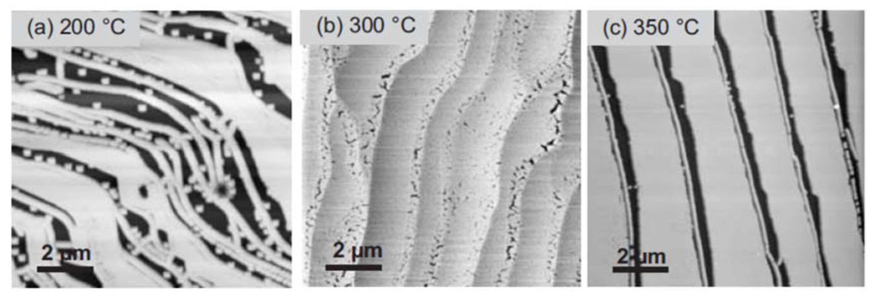
| [38] | EG growth at 1650 °C in Ar 1000 mbar, 1 L on SiC terraces, 2 L–3 L at SiC steps | None | Trimethylaluminum/H2O, 500 cycles | 200, 300, 350 | Al2O3 (50 nm), not closed | No |
| [21] | EG growth at 2000 °C in Ar 900 mbar, 1 L EG (>98%) with submicron 2 L patches | None | Trimethylaluminum/H2O, 500 cycles | 250 | Al2O3 (12 nm), closed on >98% surface | No |
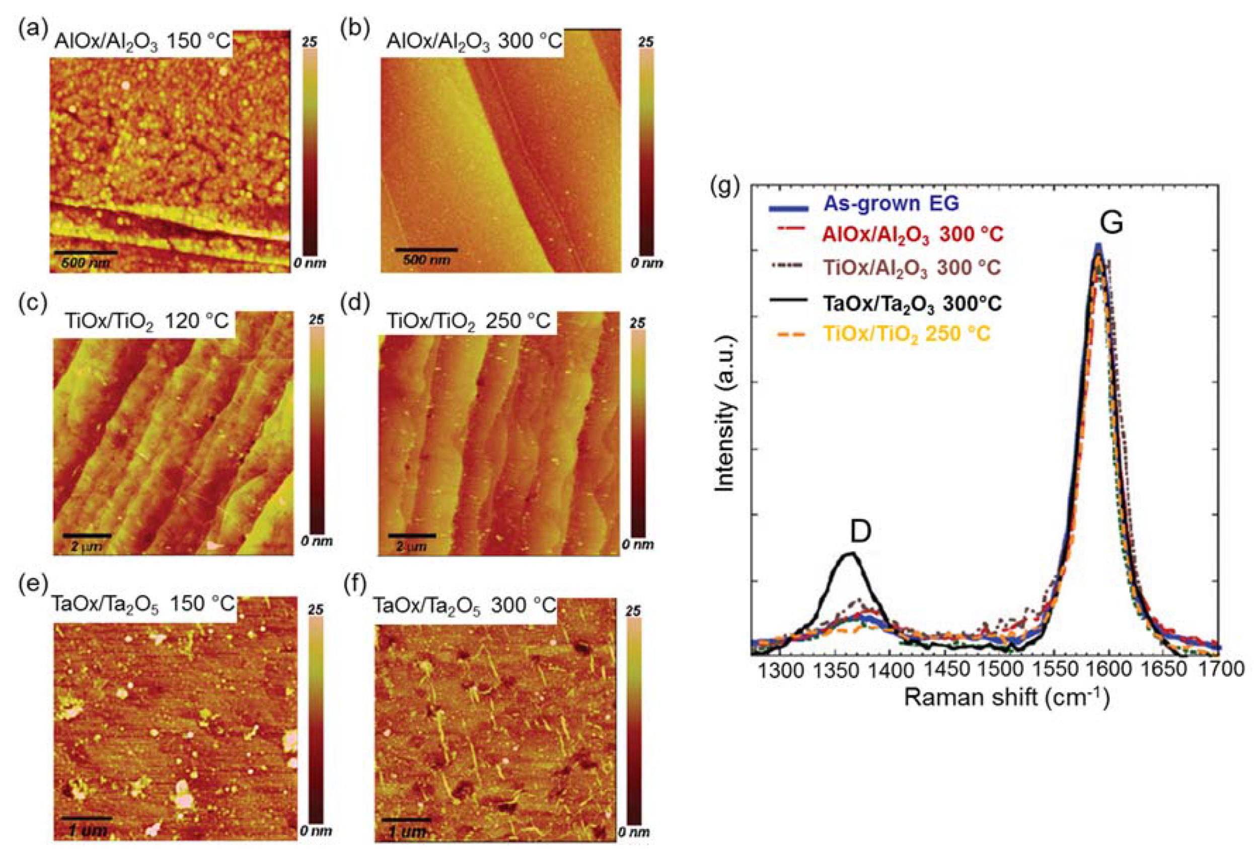
| [34] | EG growth at 1600 °C in Ar 600 Torr, 1 L to 3 L EG | Oxidized Al seed layer, 2 nm | Triethylaluminum/H2O | 150, 300 | Al2O3, closed | No |
| Oxidized Ti seed layer, 2 nm | Titanium(IV) i-propoxide/H2O | 120, 250 | TiO2, closed | No | ||
| Oxidized Ta seed layer, 2 nm | Pentakis(dimethylamino)tantalum(V) | 150, 300 | Ta2O5, closed, high roughness | Yes | ||
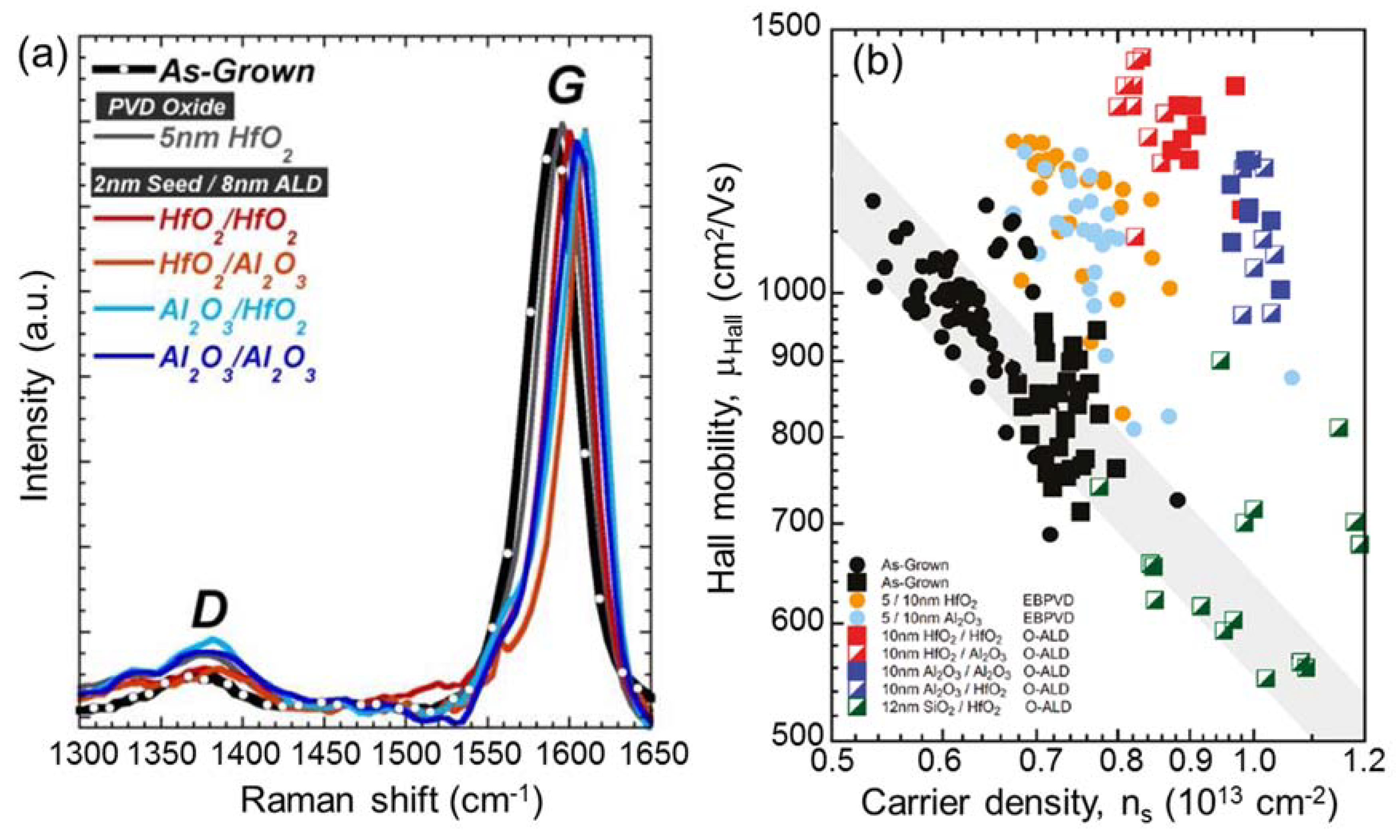
| [35] | EG growth at 1600 °C in Ar 900 mbar, Few layers EG | PVD Al2O3 seed layer, 2 nm | Triethylaluminum/H2O | 300 | Al2O3 (8 nm) + Al2O3 seed (2 nm), closed | No |
| Tetrakis(dimethylamino)hafnium/H2O | 250 | HfO2 (8 nm) + Al2O3 seed (2 nm), closed | No | |||
| PVD HfO2 seed layer, 2 nm | Triethylaluminum/H2O | 300 | Al2O3 (8 nm) + HfO2 seed (2 nm), closed | No | ||
| Tetrakis (dimethylamino)hafnium/H2O | 250 | HfO2 (8 nm) + HfO2 seed (2 nm), closed | No | |||
| PVD SiO2 seed layer, 2 nm | Tetrakis(dimethylamino)hafnium/H2O | 250 | HfO2 (10 nm) + SiO2 seed (2 nm), closed | No | ||
| [36] | EG growth at 1350 °C in UHV, mixed 1 L–2 L EG | Organic seed layer: 1 L of perylene-3,4,9,10-tetracarboxylic dianhydride (PTCDA) | Trimethylaluminum/H2O, 25 cycles | 100 | Al2O3 (2.3 nm), closed | No |
| Tetrakis(diethylamido)hafnium(IV), 25 cycles | 100 | HfO2 (2.5 nm), closed | No | |||
| [38] | EG growth at 1650 °C in Ar 1000 mbar, 1 L on SiC terraces, 2 L–3 L at SiC steps | O3 prefunctionalization at T = 250 °C | Trimethylaluminum/H2O, 500 cycles | 250 | Al2O3 (50 nm), closed | No |
| O3 prefunctionalization at T = 350 °C | Trimethylaluminum/H2O, 500 cycles | 350 | Al2O3 (50 nm), closed | Yes | ||
| [39] | EG growth at 1650 °C in Ar, 100 mbar | Fluorine prefunctionalization by XeF2 gas (from 0 to 200 s) | Trimethylaluminum/H2O | 225 | Al2O3 (~15 nm), closed | No |
© 2020 by the authors. Licensee MDPI, Basel, Switzerland. This article is an open access article distributed under the terms and conditions of the Creative Commons Attribution (CC BY) license (http://creativecommons.org/licenses/by/4.0/).
Share and Cite
Giannazzo, F.; Schilirò, E.; Lo Nigro, R.; Roccaforte, F.; Yakimova, R. Atomic Layer Deposition of High-k Insulators on Epitaxial Graphene: A Review. Appl. Sci. 2020, 10, 2440. https://doi.org/10.3390/app10072440
Giannazzo F, Schilirò E, Lo Nigro R, Roccaforte F, Yakimova R. Atomic Layer Deposition of High-k Insulators on Epitaxial Graphene: A Review. Applied Sciences. 2020; 10(7):2440. https://doi.org/10.3390/app10072440
Chicago/Turabian StyleGiannazzo, Filippo, Emanuela Schilirò, Raffaella Lo Nigro, Fabrizio Roccaforte, and Rositsa Yakimova. 2020. "Atomic Layer Deposition of High-k Insulators on Epitaxial Graphene: A Review" Applied Sciences 10, no. 7: 2440. https://doi.org/10.3390/app10072440
APA StyleGiannazzo, F., Schilirò, E., Lo Nigro, R., Roccaforte, F., & Yakimova, R. (2020). Atomic Layer Deposition of High-k Insulators on Epitaxial Graphene: A Review. Applied Sciences, 10(7), 2440. https://doi.org/10.3390/app10072440