Abstract
In this study, we designed and implemented a smart junction box (SJB) that was optimized for supplying power to low-voltage headlights (13.5 V) in electric vehicles. The design incorporated a number of automotive semiconductor devices, and components were placed in a high-density arrangement to reduce the overall size of the final design. The heat generated by the SJB was efficiently managed to mount an Intelligent Power Switch (IPS), which was used to power the headlights onto the printed circuit board (PCB) to minimize the impact on other components. The SJB was designed to provide power to the headlights via pulse width modulation to extend their lifetime. In addition, overload protection and fail/safe functions were implemented in the software to improve the stability of the system, and a controller area network (CAN) bus was provided for communications with various components in the SJB as well as with external controllers. The performance of the SJB was validated via a load operation test to assess the short circuit and overload protection functions, and the output duty cycle was evaluated across a range of input voltages to ensure proper operation. Based on our results, the power supplied to the headlights was found to be uniform and stable.
1. Introduction
As automotive technology continues to evolve from mechanical to electronic systems, consumers have started demanding higher performance products that are safer and more convenient [1,2,3,4]. At the same time, modern automobiles now include an increasing number of electronic systems, which has highlighted the need to ensure the wiring harnesses used to interconnect these systems are safe and reliable [5,6,7]. In the days when mechanical systems were primarily used, the power distribution and wiring in a vehicle were accomplished using fuse relay boxes comprising fuses and a relay. However, as the complexity of the wiring harnesses in vehicles increased with the addition of more components and joints, simple fuse relay boxes became increasingly inadequate as they require labor-intensive assembly. This was addressed by developing junction boxes that could contain more joints while enabling stacking and compactness [8,9,10]. Then, as the number of circuits in automotive wiring harnesses continued to increase along with the complexity of the control unit(s), junction boxes (JBs) were further enhanced to improve the function of the wiring harness by reducing the number of redundant power and signal lines and integrating the mounted components [11,12,13]. However, with the emergence of ever more intelligent, advanced, and eco-friendly cars designed to satisfy increasingly stringent environmental and emissions regulations, the complexity of the electronics systems in cars increased enormously, thereby significantly increasing the complexity of the wiring harnesses and junction boxes. As the functions required to improve vehicle performance have become more complicated and diverse, the length of the wires and the number of terminals in the wiring harness has increased, which has increased both the difficulty of wire placement and the likelihood of failure. A limitation is that the electronic devices in such systems must be de-integrated and tested independently via one or more operational tests to diagnose errors in their analog components. The inability to operate devices independently can compromise the safety of drivers and passengers when the control system in the car is unaware of failures and malfunctions [14,15,16].
Early JBs were developed as a simple way to connect connectors, fuses, relays, and diodes. They could be manufactured quickly and connected directly to the wiring harness. However, the disadvantages of these early types are that they used mechanical devices and wiring via crimped terminals when additional functionality was required, which increased the weight and manufacturing cost but reduced the quality. JBs can be classified as busbar, wire routed, or printed circuit board (PCB) types depending on the configuration, although the busbar type is the most common. The busbar type of JB is used to reduce the size of a terminal joint via the busbar and is widely applied in strong-current circuits that employ nonferrous metals with high electrical conductivities. However, the disadvantages of the busbar are that additional functions cannot be added easily and the devices are relatively large and heavy [17,18]. The wire-routed type can be used in applications with weak currents and provides design flexibility in diversified systems. However, this type cannot be applied in systems requiring large amounts of electrical energy. In contrast, the PCB type allows for circuit design flexibility as the circuit is constructed on the PCB itself. Other advantages of this type are that it is compact and lightweight as it relies on a direct fuse and relay.
Variations of busbar type JBs are now being developed. These JBs employ a busbar in the strong-current region and either a wire routed or PCB type in the weak-current region. However, the limitation of these JBs is that failures in electronic components are difficult to diagnose, and when separate failures occur in multiple components, users may not recognize them as failures. This problem has been solved by including a microcontroller unit (MCU) in the JB in which the software supports real-time failure diagnosis by storing and monitoring sensor and communications information. Advances in the electronic systems of vehicles have led to the development of intelligent power switches (IPSs), which are semiconductor devices designed to drive a variety of loads, such as lamps, motors, and valves. In addition to basic load switching functions, IPSs also provide overload and short-circuit protection, diagnostics, and improved electromagnetic compatibility, and are available as solderable surface-mount devices, which reduce manufacturing costs. However, as most lamps and motors in a vehicle are controlled via pulse-width modulation (PWM) signaling and receive their operating current from the IPS, the IPS needs to support both PWM signaling and monitoring via an MCU for diagnostic purposes [19,20].
These recent requirements and existing problems in JBs have led to the development of smart JBs (SJBs) that incorporate IPSs controlled via PWM to replace fuses and mechanical relays. SJBs also incorporate electronics to improve the stability of the electrical system, provide efficient power management, and enable efficient data exchange. Recent SJBs also incorporate an MCU for monitoring and control purposes. These advantages have enabled in-vehicle power distribution systems in internal combustion engine vehicles and electric vehicles (xEVs) to evolve from fuse/relay-based JBs to IPS-based SJBs. A timeline of the evolution of JBs to smart JBs (SJBs) is shown in Figure 1, and schematics illustrating the differences between JBs and SJBs are shown in Figure 2.
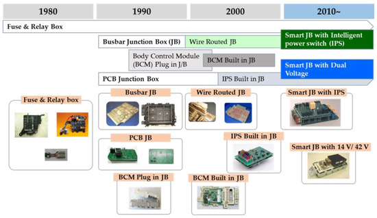
Figure 1.
Timeline showing the evolution of JBs to SJBs.
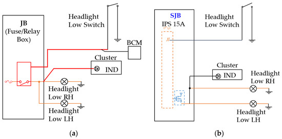
Figure 2.
Schematics illustrating the differences between JBs and SJBs: (a) JBs and (b) SJBs.
The growing adoption of xEVs has triggered a need for SJBs that can be mounted on xEVs to serve as a stable source of power [21]. However, previous studies have analyzed the results of simulations. In addition, there has been no recent research experimentally verifying the characteristics that can be seen through the manufacture of prototypes. [22,23]. In this study, we implemented a PCB-type SJB that was designed to provide stable power for the low-voltage headlights used in xEVs. A key requirement of automotive electronic systems is reliable power supply to the headlights, which is used for illumination while driving. However, this is not straightforward as the headlights are located in different places in the wiring harness, which changes the respective wiring lengths and resistances the power must traverse. If the SJB did not take this into account, the brightness of the headlights on the left and the right would not be uniform, which would compromise driver safety and may decrease the service life of the bulbs.
The PCB-type SJB in this study included a power supply and control unit that were designed to stabilize the current supplied to the headlights by controlling the duty cycle of the voltage based on the PWM signal from the SJB. The power and control units were positioned in separate locations in the SJB design to minimize any temperature-related effects. An MCU and associated software were implemented to improve driving stability by monitoring the headlights to identify any abnormal states when driving. The detection of any abnormal condition, such as open circuits, short circuits, and overvoltage, during operation, disables and resets the control system to check the load. When the input voltage is below 13.5 V, a 100% duty cycle PWM voltage is supplied to the headlights. On the other hand, when the input voltage exceeds 13.5 V, the PWM duty cycle is less than 100% to minimize the effects of the overvoltage on the headlights.
The performance of the design was validated by conducting a thermal analysis by simulating the PCB module to confirm the temperature distribution of the SJB when the headlights were driven by the IPS. Then, the PCB-type SJB was configured in a test environment in which on/off, PWM load control, protective operation, and diagnostic tests were performed.
2. SJB Implementation
2.1. Design of the SJB PCB Module
A schematic of the implemented SJB is shown in Figure 3. In this design, the PCB module consists of a dual PCB-type arrangement in which the power and control circuits are separate. The components in the system include a 16-bit MCU, a controller area network (CAN) communications controller, a multiple switch detection interface (MSDI) chip, a 9-channel IPS, a low-side driver (LSD) chip for relay control, and a power supply. The IPS was initially configured to supply and control six headlights that consume a large amount of current, although other loads, such as that of wipers, can also be added. The initial six control loads were defined as: Headlight Low (left hand (LH) and right hand (RH)), Headlight High (LH and RH), and Fog (LH and RH). The CAN module provides both low- and high-speed communications buses. The low-speed CAN bus is used for load control communications with the vehicle body control module (BCM) while the high-speed bus is used for communications with other modules, such as an electronic control unit (ECU), in support of load control and diagnostic functions. The purpose of the watchdog circuit is to monitor and reset the MCU when any of the components malfunction and to directly drive the Headlight Low Beams in such instances.
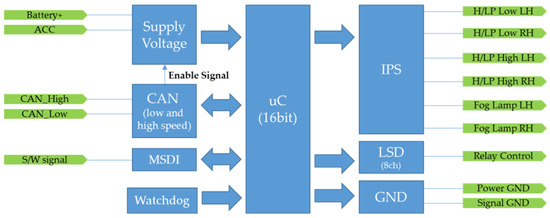
Figure 3.
Schematic of the implemented SJB.
The SJB control board receives power from the power board and is configured to control the on/off state of the load through the IPS. This board includes the following:
- Main power supply circuit: converts the 13.5 V (input) to 5 V (output), as required by the MCU,
- Control MCU: the MCU and its associated peripheral circuits,
- IPS: the IPS and the peripheral circuits required for each load capacity,
- CAN: includes one high speed and one low speed 1-channel CAN bus,
- Watchdog: circuit designed to detect abnormalities in the operation of the MCU, and
- Interface and I/O: Interface circuitry for processing external input signals and input/output circuitry to and from the other circuits in the SJB.
A detailed schematic of the main power supply is shown in Figure 4. To stabilize the power, B + 2, B + 3, and ACC power are supplied in parallel from the relay box at the rear of the battery. All three of these types of power pass through reverse voltage diodes that smooth the power before it is received at the SJB control board. The voltage regulator in this supply is a TLE4263 (Infineon) with an output voltage of 5 V and a maximum output current of 200 mA. An inhibit port is provided as a way to implement a sleep function, which limits the dark current, and the watchdog port is connected to allow the watchdog function to exert control in the MCU.
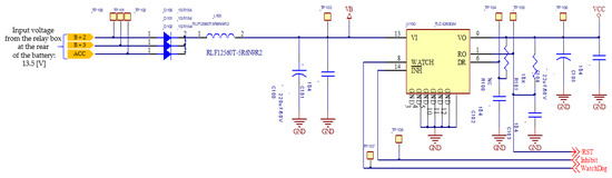
Figure 4.
Schematic of the main power supply.
The SJB power board is composed of a multi-function switch input circuit to supply power to the load through the connection with the SJB control board and to the other modules through a fuse connection. This board includes the following:
- A terminal block for connection purposes,
- A fuse for power distribution,
- Relay and driver circuits, and
- I/O expansion circuits that support connection to external input signal processors.
A schematic of the SJB power board circuitry is shown in Figure 5.
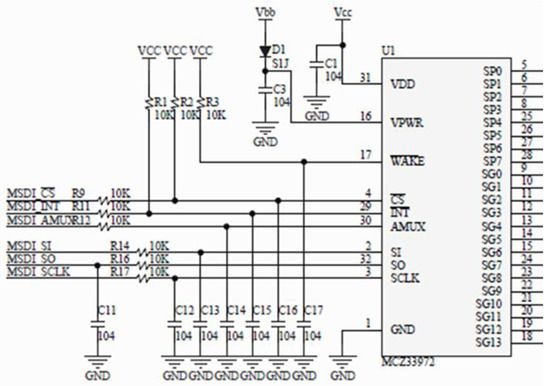
Figure 5.
Schematic of the circuitry on the SJB power board.
The specifications of the primary power, control, and communications components in the designed SJB are listed in Table 1.

Table 1.
Specifications of the main components.
The specifications of the output in terms of the loads, current consumed, and IPS are provided in Table 2.
Table 2.
Specifications of the output in terms of the load, current consumed, and IPS.
The proposed SJB includes a PCB structure consisting of power, control, and communication portions. The power and control units were placed in separate regions on the same PCB to simplify placement of the connector and fuse and to reduce the amount of noise generated by the strong current. This arrangement also reduces the potential for temperature-related problems because it allows the IPS to be placed in the upper section of the PCB. In addition, each component related to the IPS component was placed as close as possible to the load connector pins to minimize various factors, such as PCB resistance. To solve the problem due to high-density components mounting in the control section of the PCB, some of the components that were not significantly affected by noise were placed in the power section. In addition, to minimize the effects of the heat generated by the IPS components, the MCU and communication devices were placed in the lower section of the PCB. The layout of the PCB is shown in Figure 6.
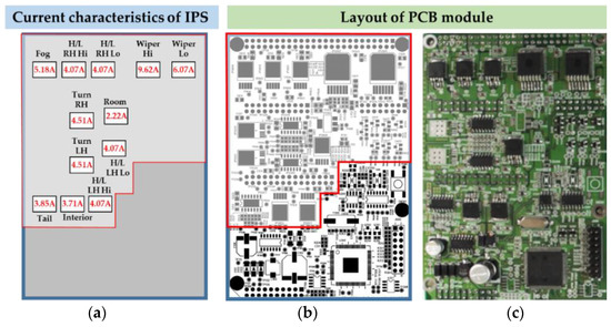
Figure 6.
Diagrams showing the PCB layout of the SJB: (a) block diagram of the IPS circuitry, (b) arrangement of the components on the board, with the IPS circuitry contained within the area outlined in red and the control circuitry contained in the lower region, and (c) photographic image of the fabricated PCB.
The developed SJB was thermally analyzed by way of a simulation to determine the heat dissipation of the IPS components when driving each load. To analyze the thermal distribution according to the behavior of the SJB PCB module, we used a commercial thermal analysis tool, PADS, and simulated the thermal distribution of the PCB module. An image of the temperature distribution is shown in Figure 7. The results of this analysis showed that under full load operating conditions with both headlights and wipers in operation, the initial maximum temperature on the board was 45.7 °C. The maximum temperature then increased to 66.9 °C when the wipers were set to high power. The temperature rise may be even higher if the SJB were to be installed in the engine compartment of a vehicle powered by an internal combustion engine; however, it is not a concern in this case as the focus of this study is on SJBs for electric vehicles. In the IPS section of the board, the components that experience higher temperatures were placed around the connector to improve the heat distribution to the connector side. In addition, the IPS component that powers the load was placed at the top of the PCB. These measures were considered to satisfactorily address any potential heat-related problems in the SJB.
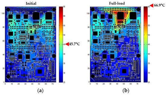
Figure 7.
Temperature distribution on the SJB PCB module: (a) initial temperature, and (b) temperature after the wipers were set to high.
2.2. Design of SJB Software
A flowchart describing the operation of the software program is shown in Figure 8. At a high level, the program operates as follows. The software first initializes the SJB and determines the current status. Then, if no error conditions are detected, the SJB switches to normal operating mode. On the other hand, if errors are detected, the software powers down the SJB by placing it into sleep mode. Detailed descriptions of each step are as follows:
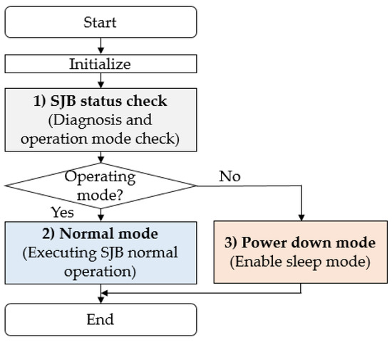
Figure 8.
Flow chart of the software.
- SJB status check: determine the status of the SJB by conducting a diagnostic check of the input voltages. If an error is detected, then switch to power down mode by using the algorithm in Appendix A.
- Normal mode: Monitor the software status and execute any requested load control commands (headlight: duty cycle control, other IPS loads: On/Off control). During IPS operation, monitor the status of the IPS by using the algorithm in Appendix B.
- Power down mode: When an error is detected, execute sleep mode and provide an error indication to the controller. Then, wait for a wake-up or reset signal to be received through the CAN bus before restarting. The algorithm executed in this step is provided in Appendix C.
The state switching diagram in Figure 9 illustrates the method used to improve the drive stability by monitoring the load to detect any abnormal states while the vehicle is being driven. The various operating states and switching conditions used in the algorithm are listed in Table 3.
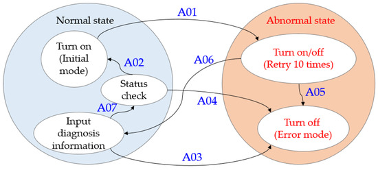
Figure 9.
State switching diagram.
Table 3.
Operating state and switching conditions used in the diagnostics routines to improve the operational stability.
The timing of the diagnostic routines is depicted in the chart in Figure 10. Because of the stronger current in the transient state in which the headlight is driven, the blind time (Tb) is placed and excluded from the diagnostic condition. If an abnormal condition (e.g., open, short, overload) is detected after initialization, the load is turned off and then on again using the load control signal. This on/off cycle is then repeated 10 more times. If no abnormal conditions are detected during repeated cycling, the IPS is allowed to resume normal operation. Otherwise, the corresponding IPS is placed into error mode, the error status is stored, and a corresponding message is transmitted to the system controller via the CAN bus. The error state can then be reset by turning off and resetting the corresponding IPS component that caused the error. The system includes a fail/safe function that automatically enables the protection function of the IPS component in the event of short-circuit or over-load conditions during which the MCU malfunctions.
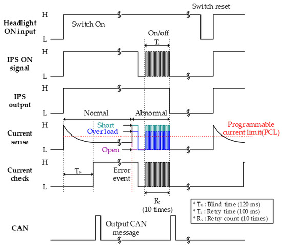
Figure 10.
Status switching to improve the operational stability by checking the abnormal state of the load during load.
The overload protection function is implemented using a programmable current limit (PCL) that monitors the supply current delivered by the IPS to the load. The range of the PCL is shown in Figure 11 and is based on the steady state current delivered to the headlights and the current handling capacity of the wire. In this implementation, the upper and lower limits of the headlights to be controlled are 150% and 50%, respectively, which in the case of the headlight loads (H/LP Low LH) were 6.111 and 2.073 A, respectively. The software program is designed to monitor the current during operation, and if a PCL limit is detected (i.e., an abnormal condition is detected), the IPS is cycled off/on 10 times to ensure the detected error was valid. If an overload or underload is detected after the 10 cycles are complete, the software program displays an error flag and terminates the IPS.
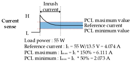
Figure 11.
Configured range of the programmable current limit.
3. Experimental Verification of the SJB
The performance of the SJB when driving the headlights was evaluated using the developed SJB PCB module and the test environment shown in Figure 12. The test environment consisted of an SJB PCB module, a power source for powering the SJB PCB module, a battery for supplying input power to the headlights, CAN communications control equipment, and a testing machine equipped with a headlight.
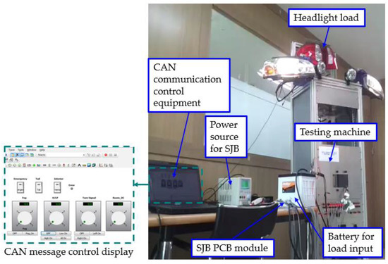
Figure 12.
Test environment.
This setup was used to assess the load driving functions of the module, to determine whether the current supplied to the headlights was uniform in the presence of supply voltage fluctuations, and to evaluate the performance of the protection and diagnostic tests.
3.1. Load Operation Test (On/Off Control)
A driving test was conducted for each headlight load to evaluate the characteristics of the load. The voltage drop was measured based on the current output by the SJB, the length of the wire, and the power consumed by the headlights. A schematic of the driving test for each headlight is shown in Figure 13. All messages were sent via the CAN communications equipment shown in the figure.
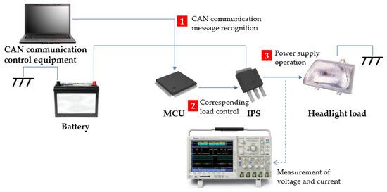
Figure 13.
Schematic of the setup used for the driving test for each headlight load.
A headlight in a vehicle has a large inrush current at startup, the consequence of which is that the headlight may burn out or its lifespan may be shortened. It also places significant electrical burden on the SJB that supplies the power. Therefore, it is important to characterize the inrush current during the initial ramp-up period via load control tests.
The current was monitored to measure the transient inrush current and steady state operating current. The measured current characteristic of the H/LP High LH output is plotted in Figure 14 in which the inrush current extended from 0 to 160 ms (denoted A in the figure). The root-mean-square (rms) value of the operating current was measured from 500 ms to 1 s after the initial drive start.
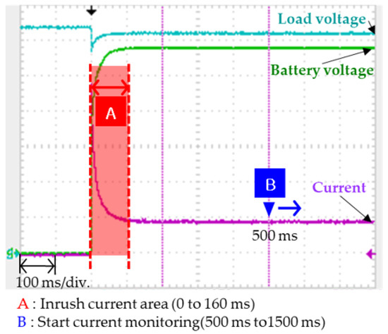
Figure 14.
Current characteristic measurement of the H/LP High LH output.
The results of the operational test for each headlight are listed in Table 4. When the headlight was turned on, a voltage drop was detected as the resistance of the wire harness differed when supplying each headlight. Therefore, there were situations in which the brightness of the headlights on the left and the right differed, which would adversely affect the life of the headlight. The benefit of PWM control is that it allows voltage fluctuations to be managed while still providing stable power to the headlights.
Table 4.
Measured characteristics of each load.
3.2. Assessing the Uniformity of the Supplied Power in the Presence of Supply Voltage Fluctuations
As explained in the previous section, when the headlights are turned on, a non-uniform drop in voltage occurs from the SJB to each headlight due to the different lengths of the connecting wire. Therefore, the power supplied by the SJB needs to be stable despite variations in the length of the wire. In addition, the capacity in the SJB needs to be sufficient to satisfy the demands of each headlight in terms of the inrush current. As this is a factor that may reduce the life of the headlight, there is also a need to tailor the driving method to prevent the headlight from experiencing premature burnout. In the proposed SJB, this was accomplished via PWM control. A schematic of the test setup used to evaluate the uniformity of the power delivered by the SJB is shown in Figure 15.
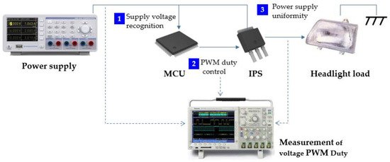
Figure 15.
Schematic of the setup used to test the uniformity of the headlight power supply.
Here, PWM control was used to vary the duty cycle of the voltage based on an input voltage of 13.5 V. The duty cycle was determined as follows:
where Vref is the input voltage reference value of 13.5 V, and Vout is the output voltage provided by the IPS to the headlight load. To reduce the headlight loss when the output voltage is too high, the following procedure was applied. When the power supply voltage is 13.5 V or less, the PWM duty cycle is set to 100%. On the other hand, when the power supply voltage is higher than 13.5 V, the duty cycle of the PWM voltage is expressed by Equation (1).
Duty cycle (%) = (Vref/Vout) × 100
An experiment was performed to measure the output duty cycle of the PWM signal supplied by the SJB to the headlight load and the resulting waveforms are shown in Figure 16. In this test, Vref was 13.5 V and the input voltage ranged from 13.5 to 16 V. The input duty of the IPS through the PWM are shown in Figure 16a–c, where it can be seen that, as the input voltage increased, the input duty cycle of the IPS decreased so as not to exceed the input voltage reference value of 13.5 V. As shown in Figure 16d–f, the output duty cycle of the IPS was the same as the voltage applied to the headlight load. The plot of the output duty cycle of the IPS shows that the PWM control output did not exceed 13.5 V, thereby preventing unnecessary energy loss in the headlight.
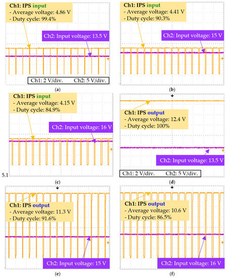
Figure 16.
Measured input voltage and IPS duty cycle (PWM waveform): (a) IPS input duty cycle at 13.5 V; (b) IPS input duty cycle at 15 V; (c) IPS input duty cycle at 16 V; (d) IPS output duty cycle at 13.5 V; (e) IPS output duty cycle at 15 V; and (f) IPS output duty cycle at 16 V.
The input and output duty cycles of the IPS for various input voltages are shown in Figure 17. As shown in the figures, as the input voltage increased, the error between the target and measured duty cycles tended to increase. In particular, the input duty and output duty cycles of the IPS were 84% for an input voltage of 16 V. Although the error between the target and measured duty cycles was 2.5%, the rms value of the IPS output voltage was 13.44 V, which satisfies the desired target (13.5 V) and does not degrade the life of the headlight.
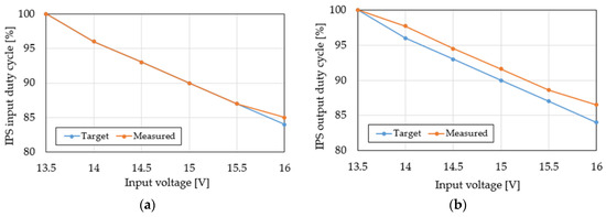
Figure 17.
Input and output duty cycles of the IPS for various input voltages: (a) IPS input and (b) IPS output.
3.3. Protection and Diagnostic Tests
Unintended open and short circuits can occur in the wiring harness connection between the SJB and the headlight. Thus, it is essential that the SJB is able to diagnose and protect against open- and short-circuit conditions. To evaluate this for the developed SJB, a protective operation and diagnostic test environment was constructed as shown in Figure 18. During testing, the open-circuit state was realized by opening a switch at the connection with the headlight, whereas the short-circuit state was configured via a switch connected to GND in parallel with the headlight.
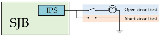
Figure 18.
Protective operation and diagnosis test environment.
The results of the short circuit test of the H/LP High RH output are shown Figure 19, where it can be seen that if VON was greater than 3.5 V when the short circuit appeared, the SJB recognized the short circuit and discontinued the supply of current.
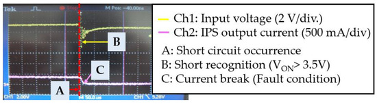
Figure 19.
Short-circuit test waveform of H/LP High RH.
The results of the tests that were conducted to assess the overload and short circuit protection capability of the SJB are provided in Table 5. A test was deemed to have been passed when the output current of the IPS dropped to 0 in the event of an open or short circuit, yet the IPS continued to operate normally. In contrast, a test was deemed to have been failed when the output current of the IPS was non-zero or the IPS itself failed to operate correctly. As shown, the SJB passed all tests.
Table 5.
Results of protective operation tests.
4. Conclusions
The increasing adoption of electric vehicles has highlighted the need for efficient methods for generating, distributing, and managing the electrical power required to drive low-voltage automotive electronic components. In this study, we implemented a PCB-type SJB designed to stabilize the current supplied to the headlights used in low-voltage electronic systems in electric vehicles. The design incorporated a number of automotive semiconductor devices, and components were placed in a high-density arrangement to reduce the overall size of the final design. Finally, the SJB was equipped with a current sensing and diagnostic system that provides the driver with the information necessary to respond to failures or unintended situations.
The heat distribution was simulated to determine the temperature distribution on the SJB module for various headlight loads. To reduce the effects of temperature on the individual circuits, the power and control units were designed as separate components and placed further apart in the module. An MCU and associated software program was implemented to monitor for abnormal states while driving the headlight load and to improve the power stability. The power loss of the headlight in the event of overvoltage was reduced by supplying PWM voltage with a variable duty cycle based on the 13.5 V power supply. In the event of the overvoltage exceeding 13.5 V, the PWM duty cycle control intervened to lower the rms value of the voltage, thereby ensuring that the voltage necessary for headlight operation is provided. A test environment was configured to evaluate the performance of the implemented SJB in terms of its on/off performance and PWM load control. Finally, a protective operation test was performed to experimentally confirm that the system was capable of diagnosing faults and of protecting the load in the event of open or short circuits.
It should be noted that the SJB PCB module developed in this study was designed to support low-voltage (13.5 V) automotive electronic loads by miniaturizing and decreasing the weight of existing JBs, improving the vehicle stability by incorporating various fault diagnosis and monitoring functions, and increasing the data transmission stability by introducing CAN communications.
In the future, we plan to apply the findings of this study to develop systems to support the high-voltage systems in electric vehicles that drive the traction motor and electric compressor by increasing the voltage and current handling capacity. We envision evolving the SJB implementation into a next generation intelligent box that integrates intelligent and high-voltage systems for driving loads in electric vehicles.
Author Contributions
Conceptualization, S.-W.B.; Methodology, S.-W.B. and S.W.L.; Software, S.-W.B. and S.W.L.; Validation, S.-W.B. and S.W.L.; Writing—original draft preparation, S.-W.B.; Writing—review and editing, S.W.L.; and S.-W.B.; Funding acquisition, S.-W.B. All authors have read and agreed to the published version of the manuscript.
Funding
This study was supported by research fund from Honam University, 2019 and the National Research Foundation of Korea (NRF) grant funded by the Korea government (MSIT) (No. 2017R1C1B5075525).
Conflicts of Interest
The authors declare no conflict of interest.
Abbreviations
| CAN | Controller area network |
| HSCAN | High speed CAN |
| LSCAN | Low speed CAN |
| MCU | Micro controller unit |
| BCM | Body control module |
| JB | Junction box |
| SJB | Smart junction box |
| IPS | Intelligent power switch |
| LS | Low-side switch |
| HS | High-side switch |
| H/LP | Head lamp |
| LH | Left hand (Left side) |
| RH | Right hand (Right side) |
| FRT | Front |
| ACC | Accessory |
Appendix A
| Algorithm A1. SJB Status Check(Diagnosis(), Mode Check()) |
| if(Diagnostic_Process() == OK) SJB_Control(); |
| else SJB_Control_Error(); |
| Ubyte Diagnostic_Process(void) |
| { |
| Ubyte ci; |
| if((giPower_LH_Analog) && (giPower_RH_Analog) < 409) ci = NOK; |
| Else ci = OK |
| Return ci; } |
| Void SJB_Control(void) |
| { |
| if(gcSJB_Status == 1) Normal_Mode(); |
| Else Power_Down_Mode(); |
| } |
Appendix B
| Algorithm A2. SJB Normal Mode(IPS Control) |
| void Normal_Mode(void) |
| { |
| IPS_Status_Chk(); |
| if((gcH_LP_sig) || (gcFog_sig)) HLP_Operating(); |
| else if(gcH_LP_sig == OFF) HLP_OFF(); |
| Else FOG_OFF(); |
| if((gcTail_sig) || (gcInterior_sig) || (gcTurnSig) || (gcEmergency) || (gcWP_INT_Mode) || (gcWP_LO_Mode)) IPS_WP_Operating(); |
| if((!gcTail_sig) || (!gcInterior_sig) || (!gcTurnSig) || (!gcEmergency) || (!gcWP_INT_Mode) || (!gcWP_LO_Mode)){ |
| if(gcTail_sig == OFF) IPS_Tail_OFF(); |
| if(gcInterior_sig == OFF) IPS_Interior_OFF(); |
| if((gcTurnSig == OFF) && (gcEmergency == OFF)) IPS_TSIG_OFF(); |
| if((gcWP_INT_Mode == OFF) && (gcWP_LO_Mode == OFF)) IPS_WP_OFF(); |
| } |
| } |
Appendix C
| Algorithm A3. SJB Power Down Mode |
| void |
| { |
| SJB_Control(void) |
| if(gcSJB_Status == 1) Normal_Mode(); |
| else Powedown_Mode(); |
| } |
| void Powerdown_Mode(void) |
| { |
| pOut_ENT = 1; |
| pOut_NSTB = 0; |
| } |
References
- Guttowski, S.; Weber, S.; Hoene, E.; John, W.; Reichl, H. EMC Issues in Cars with Electric Drives. In Proceedings of the 2003 IEEE Symp Electromagnetic Compatibility. Symposium Record (Cat. No.03CH37446), Boston, MA, USA, 18–22 August 2003; Volume 2, pp. 777–782. [Google Scholar] [CrossRef]
- Kassakian, J.G.; Jahns, T.M. Evolving and Emerging Applications of Power Electronics in Systems. IEEE J. Emerg. Sel. Top. Power Electron. 2013, 1, 47–58. [Google Scholar] [CrossRef]
- Drobnik, J.; Jain, P. Electric and Hybrid Vehicle Power Electronics Efficiency, Testing and Reliability. World Electr. Veh. J. 2013, 6, 719–730. [Google Scholar] [CrossRef]
- Yousaf, J.; Lee, D.; Han, J.; Lee, H.; Faisal, M.; Kim, J.; Nah, W. Near-Field Immunity Test Method for Fast Radiated Immunity Test Debugging of Automotive Electronics. Electronics 2019, 8, 797. [Google Scholar] [CrossRef]
- Ong, N.S.; Boothroyd, G. Assembly times for electrical connections and wire harnesses. Int. J. Adv. Manuf. Technol. 1991, 6, 155–179. [Google Scholar] [CrossRef]
- Ong, N.S. Activity-based cost tables to support wire harness design. Int. J. Prod. Econ. 1993, 29, 271–289. [Google Scholar] [CrossRef]
- Ruppert, T.; Abonyi, J. Software Sensor for Activity-Time Monitoring and Fault Detection in Production Lines. Sensors 2018, 18, 2346. [Google Scholar] [CrossRef] [PubMed]
- Evans, J.H. The Simplification of Vehicle Harness Designs through the Application of Active Junction Boxes. Proc. Inst. Mech. Eng. D J. Automob. Eng. 1990, 204, 29–33. [Google Scholar] [CrossRef]
- Afridi, K.K.; Tabors, R.D.; Kassakian, J.G. Alternative Electrical Distribution System Architectures for Automobiles. In Proceedings of the 1994 IEEE Workshop on Power Electronics in Transportation, Dearborn, MI, USA, 20–21 October 1994; pp. 33–38. [Google Scholar] [CrossRef]
- Dominguez-Garcia, A.D.; Kassakian, J.G.; Schindall, J.E. Reliability evaluation of the power supply of an electrical power net for safety-relevant applications. Reliab. Eng. Syst. Saf. 2006, 91, 505–514. [Google Scholar] [CrossRef]
- Harter, W.; Pfeiffer, W.; Dominke, P.; Ruck, G.; Blessing, P. Future Electrical Steering Systems: Realizations with Safety Requirements; SAE Technical Paper; SAE International: Warrendale, PA, USA, 2000. [Google Scholar] [CrossRef]
- Hammett, R.C.; Babcock, P.S. Achieving 10-9 Dependability with Drive-By-Wire Systems; SAE Technical Paper; SAE International: Warrendale, PA, USA, 2003. [Google Scholar] [CrossRef]
- Kim, M.; Bae, S.; Choung, S.H. Analysis on Reliability Characteristics of Power Electronic Devices for Aerial Vehicles. In Proceedings of the 2017 20th International Conference on Electrical Machines and Systems (ICEMS), Sydney, NSW, Australia, 11–14 August 2017. [Google Scholar] [CrossRef]
- Lim, H.; Park, J. Headlamp Modelling for Simulating the Capacity of Automotive Wiring Systems. Proc. Inst. Mech. Eng. D J. Automob. Eng. 2003, 217, 1043–1047. [Google Scholar] [CrossRef]
- Schmidt, C. Automotive Electronics—Enabling the Future of Individual Mobility. In Proceedings of the 2007 IEEE International Electron Devices Meeting, Washington, DC, USA, 10–12 December 2007; pp. 3–8. [Google Scholar] [CrossRef]
- Carvou, E.; Ben Jema, N.; Mitchell, B.; Gautherot, C.; Rivenc, J.; Colchen, L. Contact Behavior of Electrical Vehicle-battery Junction Box under High Shorting and Breaking Current. In Proceedings of the 26th International Conference Electrical Contacts (ICEC 2012), Beijing, China, 14–17 May 2012; pp. 151–155. [Google Scholar] [CrossRef]
- Fisher, P.; Jostins, J.; Hilmansen, S.; Kendall, K. Electronic integration of fuel cell and battery system in novel hybrid vehicle. J. Power Sources 2012, 220, 114–121. [Google Scholar] [CrossRef][Green Version]
- Nordelöf, A.; Alatalo, M.; Söderman, M.L. A scalable life cycle inventory of an automotive power electronic inverter unit-part I: Design and composition. Int. J. Life Cycle Assess. 2019, 24, 78–92. [Google Scholar] [CrossRef]
- ISO Std. 10483-1:2004. Road Vehicles—Intelligent Power Switches—Part 1: High-Side Intelligent Power Switch; ISO: Geneva, Switzerland, 2004. [Google Scholar]
- Gu, C.; Wheeler, P.; Castellazzi, A.; Watson, A.J.; Effah, F. Semiconductor Devices in Solid-State/Hybrid Circuit Breakers: Current Status and Future Trends. Energies 2017, 10, 495. [Google Scholar] [CrossRef]
- ISO Std. 7637-2:2011. Road Vehicles—Electrical Disturbances from Conduction and Coupling—Part 2: Electrical Transient Conduction Along Supply Lines Only; ISO: Geneva, Switzerland, 2011. [Google Scholar]
- Un-Noor, F.; Padmanaban, S.; Mihet-Popa, L.; Mollah, M.N.; Hossain, E. A Comprehensive Study of Key Electric Vehicle (EV) Components, Technologies, Challenges, Impacts, and Future Direction of Development. Energies 2017, 10, 1217. [Google Scholar] [CrossRef]
- Lim, H.; Jung, D.-H.; Kwon, G.; Lee, Y.J.; Park, J.S. Downsizing an automotive junction box based on large current-carrying printed-circuit board optimization. Proc. Inst. Mech. Eng. Part D J. Automob. Eng. 2017, 231, 267–278. [Google Scholar] [CrossRef]
© 2020 by the authors. Licensee MDPI, Basel, Switzerland. This article is an open access article distributed under the terms and conditions of the Creative Commons Attribution (CC BY) license (http://creativecommons.org/licenses/by/4.0/).