Abstract
Surface plasmons have been attracting increasing attention and have been studied extensively in recent decades because of their half-light and half-material polarized properties. On the one hand, the tightly confined surface plasmonic mode may reduce the size of integrated optical devices beyond the diffraction limit; on the other hand, it provides an approach toward enhancement of the interactions between light and matter. In recent experiments, researchers have realized promising applications for surface plasmons in quantum information processing, ultra-low-power lasers, and micro-nano processing devices by using plasmonic structures, which have demonstrated their superiority over traditional optics structures. In this paper, we introduce the theoretical principle of surface plasmons and review the research work related to the interactions between plasmons and excitons. Some perspectives with regard to the future development of plasmonic coupling are also outlined.
1. Introduction
Nanoscience [1] and nanotechnology [2,3] are recent revolutionary developments of science that are evolving at a very fast pace. Throughout the growth of modern optical technology [4,5], photonic device size reduction [6] and improvement of the levels of device integration [7] have been important factors in promoting the development of photonics [8]. As the feature sizes of the structures of optical devices decrease toward the nanometer scale, traditional optical methods are no longer applicable. In the new category of micro-nano photonics systems [9,10], the generation, propagation, and modulation of light and its interactions with matter have given new developments. Many unique physical and chemical properties, including quantum effects, surface effects, the macroscopic quantum tunneling effect and the microsize effect, are being discovered gradually.
As an important branch of nanophotonics, surface plasmonics [11] has allowed important breakthroughs to be made in fields involving in super-resolution imaging [12,13,14], optical sensing [15,16,17], and sub-wavelength light transmission [18,19,20,21]. Surface plasmons can achieve local sub-wavelength confinement of light fields and have a strong electromagnetic field enhancement effect within the local range of this ultra-diffraction limit. This enables nano-optical devices based on surface plasmons to control the transmission and processing of optical information at nanometer scales that are shorter than the operating wavelength, thus providing a powerful platform for the development of smaller and faster nano-optical devices that can be integrated with all-optical integration.
In addition, many special properties that cannot be predicted or represented by traditional theories [22], such as super-strong local electromagnetic field enhancement [23], super diffraction [24], polarization regulation [25], and abnormal refractive index sensitivity [26], are also being discovered regularly. These special properties offer the possibility of breaking through the limitations of traditional optics to design integrated photonic devices with a diverse range of functions and ideal performance. With different aspects of each coupling principle, especially in nanogaps, nanoparticles, and periodic gratings, these nanostructures can lead to a new class of plasmonic nanostructures and open extraordinary potentials for diverse applications, such as detection of the biological analyte, preparation of novel two-dimensional plasmonic polaritonic devices, etc.
Although it is largely explored in the research into atomic physics [27] and solid-state systems, the interaction between light and matter is one of the most important aspects of modern optical technology and plays an important role in microcavity quantum dynamics [28]. Generally, if the interaction between the emitter and its local optical environment is strong enough then the energy levels responsible for the emission are also changed, they become inextricably linked with the levels (modes) of the local optical environment. If this happens the energy levels of this hybrid system may be very different from those of the emitter or the optical system individually [29], this is the strong coupling conditions and relations. Under strong coupling conditions [30], a polariton exhibits half-laser and half-material properties.
The study opens new possibilities to explore and utilize the unique properties of hybrid states over all of the visible region down to ultraviolet frequencies in nanoscale, technologically compatible, integrated platforms based on surface plasmon technology. Starting from the basic principles, we focus here on the development of surface plasmon and exciton coupling technology in recent years, and the future trends of strong coupling between light and matter are also discussed.
2. Basic Principle of Surface Plasmons
The free electron gas [31] in a solid, when moving against a positive background of ions, may be regarded as plasma. Just as a wave of light can be quantified as a photon and a lattice vibration can be quantified as a phonon, the collective oscillation of the free electron gas in a solid’s positive ion background can be regarded as an elementary excitation that can also be quantized as a type of quasiparticle, i.e., the plasmon. As we know, the momentum matching condition can be tuned for different wavelengths by changing the incident angle of the plane wave.
Depending on their different boundary conditions, plasmons in metals can be divided into bulk plasmons and surface plasmons (SPs) [32,33,34]. Furthermore, surface plasmons can be subdivided into two categories: the first is conductive surface plasmon polaritons (SPPs), which occur at the metal-dielectric interface in the form of longitudinal waves, and the second is localized surface plasmons (LSPs), which are bound near metal structures. These three different forms are illustrated in Figure 1. As collective photon–electron oscillations makes them attractive candidates for energy applications, when light is incident on metal, it can lead to plasma oscillation inside the metal, and when the metal has boundaries, such as a metal-dielectric interface or a boundary of the metal nanoparticles’ geometry, the field will be coupled with the plasmon oscillation within the metal and will form a new oscillation mode, i.e., a conductive surface plasmon oscillation or a localized surface plasmon oscillation.
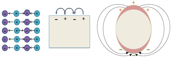
Figure 1.
Three different oscillations. Adapted from Ref. [30].
Figure 2 depicts the nanostructures of the surface plasmon polaritons (SPPs) and the localized surface plasmons (LSPs). In SPPs, the free electrons interact with the electromagnetic fields to generate dense electron waves that propagate along the metal surface [35], thus requiring one-dimensional metal structure which is close to the excited wavelength. In general, the wave vector of SPP dispersion curve is larger than that of the light while the frequency remains the same, the SPP dispersion relation can be calculated for short-pitch metal gratings for various depths, the dispersion of electromagnetic surface mode can be obtained and described by
where kspp is the wave vector of the SPP, k0 is the wave vector of the incident radiation, and ε1 and ε2 are the frequency-dependent dielectric functions of the two media on either side of the interface [36].
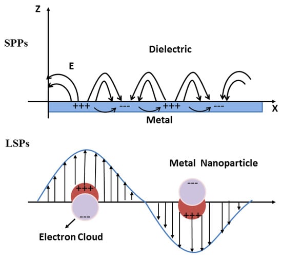
Figure 2.
Two types of nanostructure. Adapted from Ref. [35].
So it is impossible to excite plasmons with plane light waves, and some special structures are required to stimulate the SPPs, and the loss of SPPs is due to propagation [37], resulting from electron collision. Common excitation modes include prism coupling [38,39], grating coupling [40], waveguide mode coupling [41], strong-focused beams [42], and near-field excitation [43].
Moreover, the general strong coupling constant is given by [44]
where is the exciton oscillator strength, and V is the effective modal volume, m represents the free electron mass, e is the electron charge and is the dielectric constant. In addition, the momentum matching condition can be tuned for different wavelengths by changing the incident angle of the plane wave [45].
The theory here is based on the characteristics of surface plasmons when coupled with some excitons, which are confined to the metal surface on a nanometer scale and thus greatly compressed the spatial distribution of the electromagnetic field. This forms a theoretical basis for exploration of the coupling effect between surface plasmons and excitons.
3. Recent Progress in Coupling between Surface Plasmons and Excitons
3.1. Strong Coupling between Plasmons and Excitons on Conductive Surfaces
In the common strong coupling system, the most basic components are the optical resonators and the excitons. To achieve strong coupling, it is necessary to increase the coupling strength while reducing the rates of attenuation and decoherence in each component. Therefore, it becomes increasingly important to select appropriate components for the coupling system. The study of the interactions between surface plasmons and excitons dates as far back as 1902. The Wood group [46] in London observed narrow-band anomalous diffraction in the reflection spectra of metal gratings for the first time. Zenneck [47] and Sommerfeld [48] then provided a mathematical description of the surface waves that were transmitted along the surface of a conductor with finite conductivity. In 1941, Fano [49] connected the abnormal diffraction phenomenon that occurred in metal gratings with Sommerfeld’s previous theoretical work and developed the theory of Wood’s anomalous diffraction gratings before proposing the concept of the surface plasmon wave (SPW). However, it was not until 1957 that Ritchie [50] described the conduction electrons using the hydrodynamic Bloch equations; he found that, in very thin idealized foils, energy loss may occur with a value that was less than the plasma energy, and also demonstrated that this behavior was related to the metal film interface when the foil thickness decreased below v/wp, where v and wp were the velocity and the plasma frequency, respectively. Powell’s group [51] found that the general changes in the loss spectra and the specific changes in the spectrum of aluminum showed good agreement with the predictions of Ritchie. In the same year, Stern et al. [52] first proposed the concept of surface plasmons. Otto [53] discovered that if a prism is brought close to a metal-vacuum interface, surface plasma waves can be excited optically using the evanescent wave present during total reflection, and the excitation of surface plasmons by attenuated total reflection, i.e., the Otto model, was then proposed. Kretschmann and Raether [54] subsequently improved Otto’s structure and the surface plasmon wave was successfully excited at the interface between a metal and another medium via the prism coupling method. A unified theoretical explanation for surface plasmon theory was thus established.
In 1982, Pockrand et al. [55] studied exciton-surface plasmon interactions using attenuated total reflection spectroscopy. They used Langmuir-Blodgett monolayer assemblies that contained dye molecules and had been deposited on silver films to form Kretschmann structures; these characteristic structures appeared at the transverse exciton frequency because of the interaction of the SPPs with the component of the dye transition dipole moment oriented parallel to the surface. While the angle remained unchanged, the reflection spectrum was obtained using the different wavelengths that were used to excite the SPPs, and the anticrossing dispersion relationship in the coupling system was also obtained. This showed that the coupling strength between the SPPs and the excitons could be adjusted by varying the spacing of the silver film and the molecular thin layer.
During later research in 2004, Bellessa et al. [56] performed reflectometry experiments on an organic semiconductor composed of cyanide dye J-aggregates deposited on a silver film, as illustrated in Figure 3. They observed the dispersion lines that represented an anticrossing, which is the signature of strong plasmon-exciton coupling. In addition, the Rabi splitting characteristic of their coupling reached 180 meV at room temperature. The emission of the low energy plasmon-exciton mixed state was also observed and showed a considerable shift from the corresponding uncoupled emission.
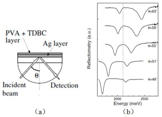
Figure 3.
(a) Layout of reflectometry experiment showing the sample and the BK7 hemispherical prism. (b) Reflectometry spectra for various angles as a function of the incident light energy [56].
In analogous experiments in 2005, Dintinger et al. [57] at the Université Louis Pasteur studied the interaction of a J-aggregate and the SPP modes of a subwavelength hole array in detail. By measuring the effects of the hole array period, the angular dispersion and the J-aggregate concentration on the transmission of the array, the existence of a strong coupling regime was demonstrated with Rabi splitting energy of 250 meV. Additionally, the splitting energy was expected to vary with the square root of the absorbance. The results, which are plotted in Figure 4b, showed very good agreement with the previously predicted square root dependence.
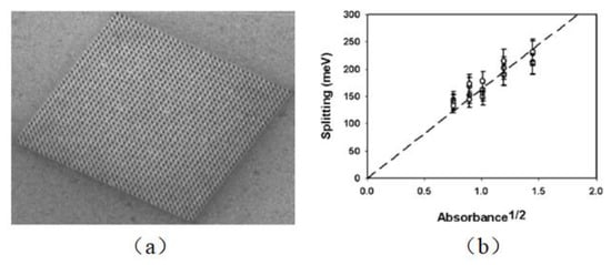
Figure 4.
(a) Scanning electron image of typical hole array milled into a silver film. (b) Variation of Rabi splitting as a function of the square root of the absorbance of the J-aggregate/polyvinyl alcohol (PVA) film [57].
In 2006, in a similar manner to the work of Dintinger et al., Bellessa et al. [58] described the properties of organic semiconductor excitons during strong interactions with surface plasmons, and the dependence of the Rabi splitting on the square root of the dye layer absorption and the width inversion of the reflectometry lines at resonance were both observed. The Rabi splitting is shown as a function of the calculated absorption in Figure 5b and shows a linear dependence in the same way as the Rabi splitting when plotted as a function of the experimental dependence, but with a higher rate. Comparable reports about strong coupling between metal films and excitons can be found in the related literature [59].
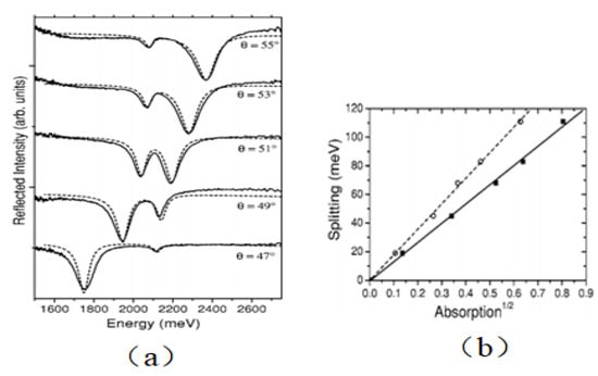
Figure 5.
(a) Reflectometry spectra of PVA (polyvinilalcohol)-TDBC (the 5,5′,6,6′-tetrachloro-1,1′-diethyl-3,3′–di(4-sulfobuthyl)-benzimidazolocarbocyanine) layer on silver at various detection angles as a function of the incident light energy. (b) Filled squares represent the experimental Rabi splitting values as a function of the square root of the experimental absorption of the PVA-TDBC layer, while the open circles represent the Rabi splitting as a function of the square root of the calculated absorption [58].
In addition to the J-aggregates-based composite system, the surface plasmon effect has also been explored in graphene composite systems [60], mainly for application to the fields of biological detection and analysis. It was not until 2010 that a graphene covering over a gold sensor membrane was first reported to enhance the surface plasmon resonance (SPR) detection signals. Wu et al. [61], at the Institute of High Performance Computing in Singapore, presented an SPR biosensor based on a graphene-on-gold structure; Figure 6 shows their structure, where the gold surface was covered with an SF10 glass prism. With the aim of achieving greater SPR signal amplification, increasing numbers of researchers have combined various types of nanomaterials, including graphene oxide decorated with gold nanorod-antibody conjugates [62], graphene oxide coupled with gold nanoparticles [63], multilayer graphene structures, and silicon coatings on gold films [64].
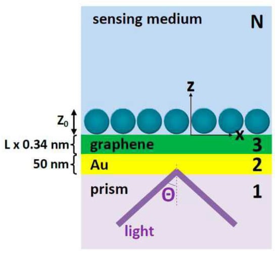
Figure 6.
N-layer model for surface plasmon resonance (SPR) biosensor: prism | Au (50 nm) | graphene (L × 0.34 nm) | sensing medium, where L is the number of graphene layers, and z0 = 100 nm is the biomolecule layer thickness [61].
Lee et al. [65] showed that a composite material that consisted of a graphene sheet on an Au (111) surface exhibited both excellent conductivity and the ability to adsorb biomolecules stably. Remarkably, the signal-to-noise ratio of this structure was so high that the resonant currents passing through the different nucleobases were clearly distinguishable.
Li et al. [66] proposed a novel Ag nanoparticles (NPs) and Ag film (named the G (graphene)–NFG system) gap by introducing an ultrathin graphene monolayer as a well-defined sub-nanospacer between Ag NPs and a Ag film. This new G–NFG system offered tremendous near-field enhancement with one of the highest enhancement ratios (1700) reported to date and is illustrated in Figure 7.
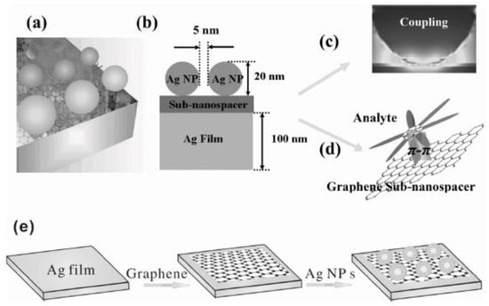
Figure 7.
(a) 3-dimensional schematic of the G-NFG system. (b) Cross-sectional schematic of the G-NFG system. (c) Strong near-field due to NPs-film coupling. (d) Chemical mechanism enhancement. (e) Schematic of the fabrication process of the graphene separated G–NFG system. [66].
Yong et al. [67] used a graphene-gold metal-surface composite structure to improve the sensitivity of a DNA detection structure effectively. (In systems based on coupling of excitons and SPPs, relevant studies were also performed on surface-enhanced Raman scattering (SERS), DNA detection and other aspects.)
Chen et al. [68] successfully achieved the integration of plasmonic Al NPs with wrinkle-like graphene sheets and obtained experimental Al nanoparticle-enhanced solar cells. As shown in Figure 8, the structure effectively enhanced the device absorption of the ultraviolet band while increasing the limiting effect on light, and thus ultimately improved the device efficiency.
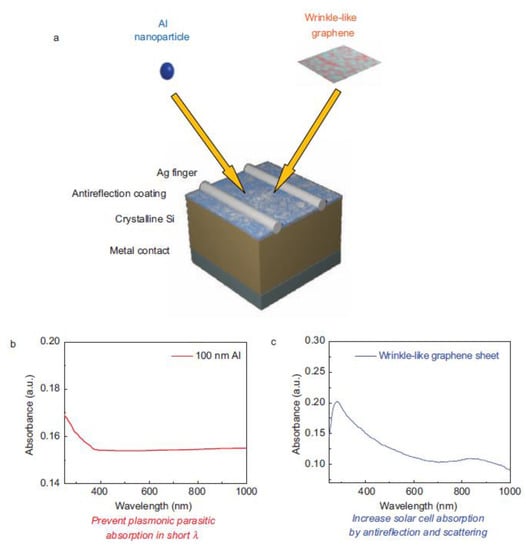
Figure 8.
Illustration of proposed textured Al nanoparticle/graphene-enhanced screen-printed solar cell [68].
Strong coupling of the conductive surface plasmons and excitons has been achieved gradually by varying the distance between the thin layer of molecules and the metal surface.
3.2. Strong Coupling between Plasmons and Excitons on Localized Surfaces
While strong coupling between inorganic semiconductor materials and light at room temperature is possible, fine-grained microcavities are still required. When the surface isoionization excimer is introduced, the electric field intensity around it is greatly enhanced because the mode volume is very small and the light is localized within the subwavelength range. In addition, use of high concentrations of molecules or quantum dots can increase the effective dipole moment. Therefore, strong coupling between matter and localized surfaces has become a hot research topic.
In 2009 and 2011, the Rabi splitting value reached 450 meV [69] and 650 meV [70], respectively, which already represented the super-strong coupling zone. After the introduction of surface plasmons, Rabi splitting could be observed without use of a closed cavity at room temperature. Figure 9 compares the weak and strong coupling between an optical cavity with resonant LSP modes supported by metal nanoparticles [71].
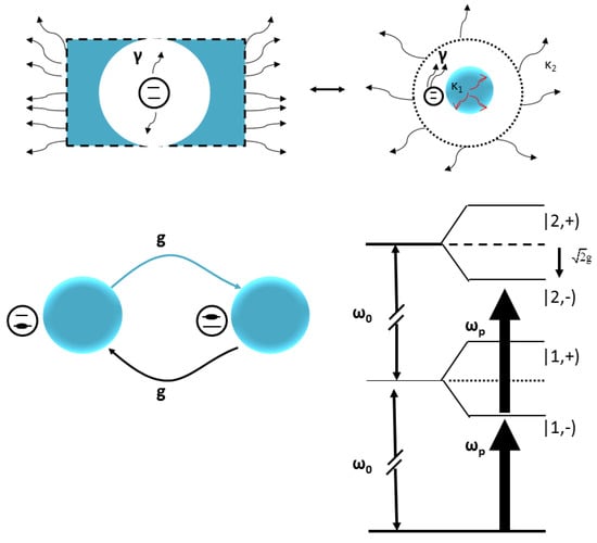
Figure 9.
Weak and strong coupling. Adapted from Ref. [71].
Strong coupling is more easily realized in molecules with narrow absorption spectra such as J-aggregates, depending on the coupling conditions. However, strong coupling could also be obtained in SP nanostructures and molecules that have broad absorption spectra. In 2009, Hakala et al. [72] reported two types of experiments. Initially, the surface of a Ag film was covered with a poly (methyl methacrylate) (PMMA) film containing Rhodamine 6G, and the reflection spectrum of the structure was measured using a Kretschamann-Raether (K-R) structure. The resulting curve showed a significant anticrossing, and the size of the Rabi split increased linearly as the square root of the molecule concentration increased, resulting in a Rabi splitting energy of up to 230 meV. Then, by varying the thickness of the PMMA layer, which affects the coupling time of the SPPs and the molecules directly, increased coupling strength was realized.
Nagasawa et al. [73] performed polarized Raman scattering measurements using a hybridized system composed of Ag nanodimer structures and organic dye molecules. The energy of the hybrid polaron in this system could be regulated by adjusting the LSP energy. The energy of the surface plasmon could also be adjusted by varying the spacing of the paired Ag particles. The anticrossing behavior of the polariton energy indicated a strong coupling regime and a maximum Rabi splitting energy of 39 meV. Most importantly, effective Raman enhancement could be obtained by exciting the high and low levels of the hybrid state within the gap between the paired metal particles, and the maximum Raman enhancement was located at an optimized resonant energy between the hybrid states and the Raman excitation energy. This was the first study of Raman enhancement caused by LSPs coupled with dye molecules.
In addition, to enhance the interactions between light and matter, growing numbers of research teams have begun to use the subwavelength confinement properties of metal NPs and nanocavity surface plasmons [74]. In the earliest work on strong coupling of local surface plasmons and excitons, Baumberg et al. [75] reported the first observation of polaritonic spectral narrowing and strong coupling between localized plasmons and J-aggregate excitons with a Rabi splitting energy of 230 meV at room temperature, as illustrated in Figure 10.
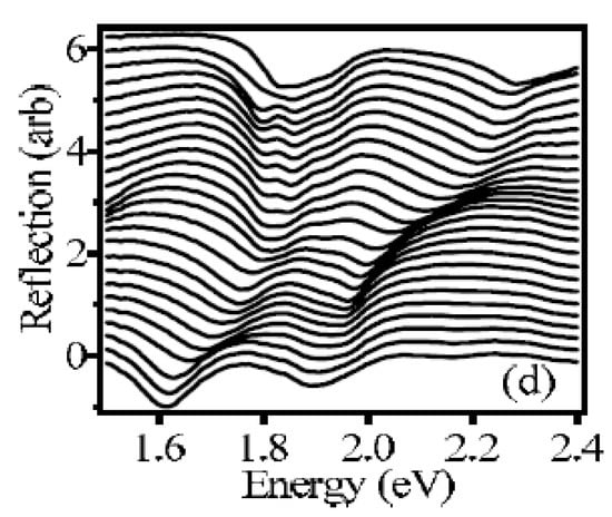
Figure 10.
Normal incidence reflectivity vs. void thickness for a 20 nm J-aggregate film [75].
Since then, both theoretical and experimental work on LSP Resonances (LSPRs) and exciton coupling has continued to emerge. Researchers have demonstrated strong interactions between plasmons and excitons in various particle-exciton material systems, including use of gold or silver NPs with various shapes, such as nanoshells, nanorods, nanostars, and nanotips. Figure 11a–c depict the near-field distribution contours of silver nanospheres, nanotriangles, and nanorods, respectively [76]. The figures illustrate that the electric field enhancement of the single particle structure is weak and the enhancement factor is basically in the 1–100 range. To improve the enhancement by multiples of the near field, a coupling structure can be adopted; in Figure 11d, a silver nanosphere dimer has a maximum enhancement factor of 338. Similarly, the silver nanocube over mirror system in Figure 11e has a maximum enhancement factor of 450. These figures show that the near field distribution, the enhancement and the far field emission directions of surface plasmons can be adjusted flexibly by designing the structural characteristics of the surface plasmon nanostructure.
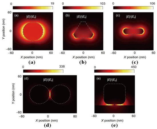
Figure 11.
Electromagnetic calculations of near-field distributions of different silver nanoparticles. (a) Nanosphere (diameter 60 nm) with a maximum field enhancement factor of 19; (b) nanoprism (edge: 60 nm; thickness: 20 nm) with a maximum enhancement factor of 103; (c) nanorod (length: 60 nm; width: 15 nm) with a maximum enhancement factor of 106; (d) silver nanosphere dimer (diameter: 60 nm; gap: 2 nm) with a maximum enhancement factor of 338; (e) silver nanocube over mirror system (cube side length: 65 nm; gap: 3 nm) with a maximum enhancement factor of 450. The gap modes of the coupled systems in (d,e) have stronger field enhancement when compared with the single nanoparticle plasmon modes in (a–c) [76].
Figure 12 illustrates some typical research work on strong interactions between LSPRs and excitons. Shegai et al. [77] demonstrated strong coupling between plasmons that were confined within a single silver nanoprism and excitons in molecular J-aggregates under ambient conditions through single-particle dark-field scattering measurements. They estimated that the number of excitons that contributed coherently to the coupling process was N~70−85, thus implying that single exciton strong coupling may be within reach as a result of further compression of the mode volume shown in Figure 12a. In their subsequent work, by improving the samples, the J-aggregates were wrapped uniformly around the silver nanotriangle and the redundant uncoupled molecules were removed; splitting was not only obtained on the scattering spectrum, but also was observed on the fluorescence spectrum, as seen in Figure 12c [78]. Figure 12b shows the interactions between the J-aggregate excitons and the single plasmonic dimers, and the splitting of the peak pattern can also be observed in the scattering spectrum [79].
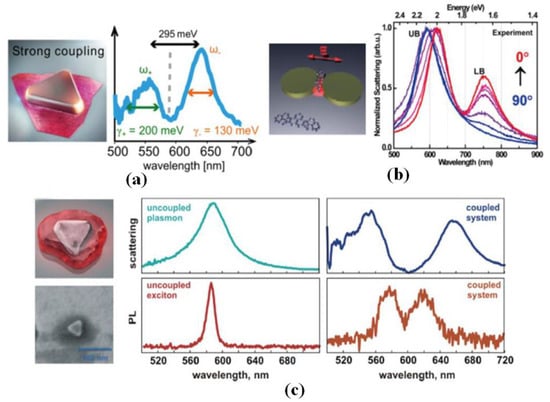
Figure 12.
(a) SEM image of the prism and scattering spectrum of single nanoprism strongly coupled to J-aggregates [77]. (b) Structure diagram between J-aggregate excitons and single plasmonic dimers and polarized scattering spectra of plexcitonic dimer with detected polarization different angles [79]. (c) SEM images of the nanoparticles imaged on top of Au surface to visualize J-aggregate shell and the scattering spectums of uncoupled and coupled system [78].
Apart from the J-aggregates and dyes, strong coupling has also been achieved between photochromic molecules and surface plasmons. The photochemical effect can be used to vary the configuration of the molecule, which in turn changes the coupling strength between the molecule and the light field, thereby achieving a reversible transition between weak and strong coupling. The light-molecule interaction in a cavity containing photochromic spiropyran molecules is a reversible process and is optically addressable, which allows for fine control of the coupling conditions [80]. Active control of the coupling strength between porphyrin dyes and SPPs is supported by a thin gold layer; this control is reversible. The coupled system changes from weak coupling to the strong coupling regime (Rabi splitting of 130 meV) by controlling the effective oscillator strength in the dye layer through exposure to nitrogen dioxide [81].
Gómez et al. [82] presented an experimental demonstration of the strong coupling between a surface plasmon propagating on a planar silver thin film and the lowest excited state of CdSe nanocrystals, which was characterized by a Rabi splitting energy of 112 meV at room temperature. They also studied the quantum electrodynamics in the cavity. Additionally, for the dipole moment of the transition of a single optical emitter material, e.g., perovskites [83,84], dye molecules and excitons in semiconductors, any type of optical transition that is associated with a given oscillator strength can be used for reaching the strong coupling regime [85]. For a general single-particle surface plasmon and a single emitter-coupled composite system, the whole system cannot achieve strong coupling; therefore, a strong coupling effect with the single emitter can only be achieved using the gap mode, with its stronger local limiting effect on the light.
In 2016, Chikkaraddy et al. [86] showed that photon emitters placed in an optical cavity experienced an environment that changed how they were coupled to the surrounding light field; this was called the nanoparticle-on-mirror (NPoM) geometry. The assembly of the so-called NPoM structure involved placement of particles on the gold film and addition of methylene blue dye to the gap between the particles and the gold film. The gap mode formed by this system is similar to the gap mode between two vertical spherical dimers. In this mode, the plasmon’s binding properties to the subwavelength of the light are effectively improved, while the mode volume is reduced, and the electric field intensity in the gap is enhanced. Simultaneously, they used chemical methods to cause the orientation of the dye molecule’s transition dipole moment to be parallel to the direction of the strongest electric field, and strong coupling between a single optical emitter and the surface plasmon nanoresonator was finally achieved, as illustrated in Figure 13.
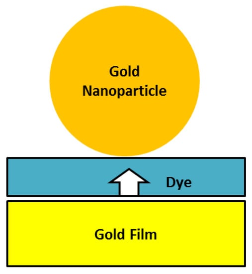
Figure 13.
Diagram of NPoM structure. Adapted from Ref. [86].
Current research tends toward enhancement of the strong coupling between local surface plasmons and excitons using the subwavelength binding characteristics of the metallic NPs and the microcavity surface plasmons [87].
3.3. Strong Coupling between Metal Periodic Structure Plasmons and Excitons
At present, researchers are focusing on how to study the strong coupling effect in the quantum optics field using a single plasmon nanoscale resonator and a strong interaction system of excitons. However, because of the limitations of the manufacturing processes or the test methods, some of the strong coupling phenomena are difficult to observe experimentally. Therefore, periodic nanostructures, e.g., metal nanoparticle arrays or gratings, are used to study the strong interactions between light and matter because they offer unique advantages. A periodic array of metal nanostructures can form hybrid LSP resonance modes and diffraction modes under near-field interaction conditions [88], which are called surface lattice resonances (SLRs). When compared with pure plasmon nanoresonators, the advantages of these SLR modes are obvious: for example, Fano interference between the plasmon mode and the diffraction mode will produce a higher quality factor, and mode dispersion is produced by the two-dimensional periodic structure. The exciton emission can also be modulated effectively using a periodic plasmon structure and exciton coupling.
Pompa et al. [89] developed a new strategy based on highly reproducible fabrication of ordered arrays of gold nanostructures coupled to CdSe/ZnS nanocrystals that were dispersed in a polymer blend; periodic triangular Au particle arrays were prepared that enhanced the fluorescence intensity of CdSe/ZnS quantum dots by 30 times, as shown in Figure 14. They dispersed the CdSe/ZnS quantum dots into PMMA colloids and used the PMMA as an isolation layer (approximately 35 nm thick) to regulate the distance between the metal and the fluorescent quantum dots and thus eliminate the effects of nonradiative energy transfer. In addition, they also compared the fluorescence enhancement effects of both triangular Au particle arrays and cylindrical particle arrays on quantum dots and found that the fluorescence enhancement effect of the triangular Au particles with their periodic structure was better than that of the cylindrical particles: this was caused by a hot spot effect, where the local electromagnetic field was located at the tips of the particles and the field enhancement effect was greater. Song et al. [90] used the coupling of LSPs and SPPs to achieve an improved enhancement effect. They used CdSe/ZnS quantum dots with PMMA mixed films as masks to fabricate a cylindrical hole array by electron beam etching technology, and the Ag NPs were then interconnected using a continuous Ag thin film. Tuning of the SPP resonance to the quantum dot exciton emission band results in an up to 50-fold enhancement in the overall fluorescence efficiency, which is illustrated in Figure 14b.
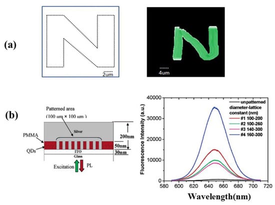
Figure 14.
(a) Triangular Au particle array produced by electron beam etching and the fluorescence enhancement effect. Adapted from Ref. [89]. (b) Schematic of typical finished sample structure and its fluorescence spectra [90].
Thomas et al. [91] detected high fluorescence enhancement and Raman scattering on periodic nanopore arrays by tuning the diameters of the nanoholes using a simple plasma etching process, with results as shown in Figure 15. Additionally, the appearance of hybridized states in the presence of excitonic molecules (RG6) led to anticrossing behavior in extinction spectroscopy; this phenomenon, which is also known as Rabi splitting, also indicated that there was strong coupling between the plasma state and the molecular exciton.
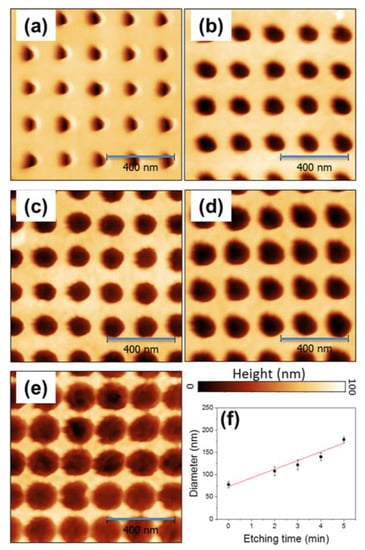
Figure 15.
Atomic force microscopy (AFM) images of fabricated polyacrylonitrile PAN nanohole structures with etching times of (a) 0, (b) 2, (c) 3, (d) 4, and (e) 5 min. (f) Nanohole diameters as a function of etching time. The red line corresponds to a linear fit of the data [91].
Salomon et al. [92] investigated strong coupling interactions between the molecules and plasmons in a mixed system composed of metal plasmon spatial arrays and polydimethylsiloxane (PDMS) films doped with porphyrin J-aggregates. Figure 16 shows the strong coupling results. Additionally, the work also demonstrated that hybrid light–matter states with greater Rabi splitting could be achieved when using plasmonic nanostructures with higher symmetry and periodicity.
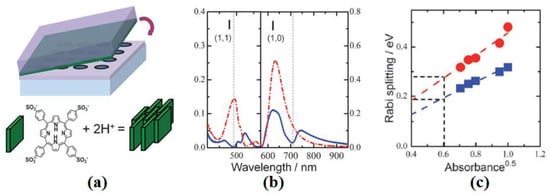
Figure 16.
(a) Schematic of sub-wavelength hole array milled in silver film on a glass substrate; adsorbed J-aggregated H4TPPS2−/PDDA bilayers grown on a polydimethylsiloxane (PDMS) slab are added on top of the array. (b) Normal incidence transmission of a square hole array (period: 330 nm) when bonded to a 1-mm-thick PDMS slab (red curve) and when bonded to a PDMS slab with J-aggregated H4TPPS2−/PDDA bilayers with absorbance of 0.898 at 491 nm (blue curve). (c) Rabi splitting values as a function of the square root of the J-aggregate absorbance at 491 nm for both hexagonal (circles) and square arrays (squares) [92].
Pan et al. [93] optimized the optical transmission properties of the structure using the angles between the central hole and the side holes, the polarization angle of the incident light, and the structural parameters (i.e., the central hole and side hole diameters, the structural thickness, and the space between the side holes and the central hole). Further analysis of the variation of the peak transmission under different refractive index conditions indicated that their structure had high sensitivity to the refractive index of the surrounding environment.
Overall, the surface lattice resonance mode in periodic structures provides a good test platform for cavity polarizing devices. The periodic surface plasmon diffraction mode and the polaritons formed by coupling of excitons have nonspatial locality characteristics that can be used for coherent energy transfer within the lattice range of the plasmon; in addition, spatial coherence can also be observed in such systems. Further studies of nonlinear optics in coupled systems were also performed, based on a similar periodic plasmon structure and exciton coupling system.
3.4. Strong Coupling between Surface Plasmons and Transition Metal Dichalcogenides
Recently, transition metal dichalcogenides (TMDs), with their excellent electrical and optical properties, were regarded as ideal candidate materials for realization of a strong coupling regime because of their high absorptivity. The strong coupling phenomenon based on use of monolayer TMD materials and single-particle plasmon nanoresonators has only been discovered gradually. Agarwal et al. [94] demonstrate the evidence of strong coupling between surface plasmon polaritons and MoS2 excitons involving three types of resonances for the first time. In the same year, Ebbesen et al. [95] provide the unambiguous signature of WS2 monolayer strong coupling in easily fabricated metallic resonators at room temperature, which suggests many possibilities for combining light−matter hybridization with spin and valleytronics. In addition, the different sizes and shapes of the NPs and the TMD states caused different fluorescence characteristics to appear, including fluorescence enhancement, unchanged fluorescence, and fluorescence quenching.
Rabi splitting based on TMD materials [96] has also been reported in a series of optical microcavity systems. Landobasa et al. [97] proposed a continuous transition from weak coupling to strong coupling between the excitons in a molybdenum disulfide (MoS2) monolayer and highly localized plasmons in an ultracompact nanoantenna at room temperature. The interactions between the excitons and plasmons were then directly prompted toward the strong coupling regime by reducing the thickness of the spacer layer, and 190 meV Rabi splitting was observed. The monolayer characteristics of the MoS2 was confirmed by atomic force microscopy (AFM), as shown in Figure 17a, while Figure 17b shows the individual NCoM constructs, which are observed as diffraction-limited, bright and colorful point scatterers in the dark field images under white lamp illumination.
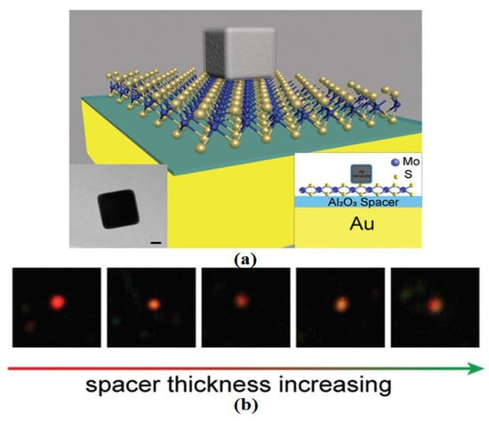
Figure 17.
(a) 3D illustration of NCoM cavity encapsulating monolayer MoS2 flakes. (b) Tunability of plasmonic cavity resonance in NCoM systems [97].
Lepeshov et al. [98] addressed the issue of resonance coupling in hybrid exciton-polariton structures based on single Si NPs coupled to monolayer (1L)-WS2. They found that when monolayer tungsten disulfide was added to the silicon NPs, strong coupling was generated at the magnetic optical Mie resonance and the Rabi splitting energy exceeded 110 meV. Additionally, when they changed the surrounding dielectric material from air to water, this led to a Rabi splitting energy of up to 208 meV. This demonstrated that optical resonance sphere coupling tunability could be achieved for the silicon nanoparticles with the addition of the monolayer tungsten disulfide.
Abid et al. [99] investigated the interference between the plasmonic and excitonic resonances in hybrid MoSe2@Au nanostructures composed of monolayer MoSe2 supported by Au nanodisks, with results as shown in Figure 18. They used a coupled oscillator model to extract the relationship between the interaction energy and the temperature and obtained a plasmonic-excitonic interaction energy of 42 ± 8 meV in the Fano-type regime.
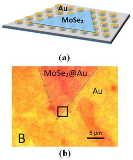
Figure 18.
Typical MoSe2 flake transferred to Au nanodisk arrays. (a) Schematic showing the MoSe2 monolayer coated on top of the Au nanodisk array on a SiO2 substrate. (b) Bright field optical microscopy image (50× magnification) of MoSe2 monolayer transferred to Au nanodisk array and fabricated using the shaped nanosphere lithography process [99].
Cuadra et al. [100] reported on the strong interactions between localized surface plasmons in silver nanoprisms and the excitons and trions in monolayer tungsten disulfide (WS2). Their temperature-dependent single-particle scattering spectrum test demonstrated the strong coupling behavior of the neutral exciton and the charged three-particle states, trions, and the silver nanotriangular plasmon in the system. In particular, they demonstrated that a stable trion state emerged and then coupled efficiently to the plasmon resonance at low temperatures by forming three bright intermixed plasmon-exciton-trion polariton states, as depicted in Figure 19.
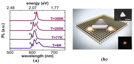
Figure 19.
(a) Photoluminescence (PL) spectra of WS2 monolayer as a function of temperature. (b) A high density of photonic states (hot spots) is shown at the corners of the nanoprism, which overlaps with the WS2 monolayer for efficient plasmon-exciton interactions [100].
It is possible to reduce the number of excitons further to a few or even to one by using TMDs as the coupling system for the exciton materials [101], and this truly reaches the scope of quantum optical research. Therefore, studies of isolated single exciton layered materials have also attracted research attention.
Xu et al. [102] constructed a single-atomic-layer tungsten diselenide hybrid system with a high length-diameter ratio for a silver bar with a low-loss third-order mode and a high vibronic strength exciton using a single particle scattering spectrum, and room-temperature formation of plexcitons with Rabi splitting energies as large as 49.5 meV was observed, as shown in Figure 20. This was also the first time that the strong interaction between the surface plasmon and the monolayer tungsten diselenide exciton was achieved at room temperature in this complex system.
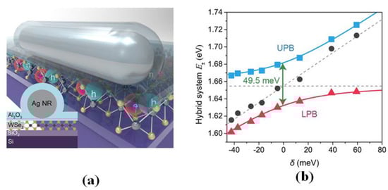
Figure 20.
(a) Schematic of system with a single silver nanorod on a WSe2 monolayer. (b) Energies of the upper plexciton branch (UPB) (E+, blue square) and the lower plexciton branch(LPB) (E−, magenta triangle) as a function of the detuning [102].
In addition, Kuipers et al. [103] demonstrate the valley-dependent directional coupling of light using a plasmonic nanowire–tungsten disulfide (WS2) layers system and Cyriaque Genet et al. [104] demonstrate valley contrasting spin-momentum locked chiralitonic states in an atomically thin TMD semiconductor coupled to a plasmonic optical spin-orbit resonator at the same time in 2018, which both represent an important new research to the potential applications of TMDs at the nanoscale.
The interest in single layers of TMDs is focused on their exceptional optical properties: the strong exciton binding energy and transition dipole momentum, large spin−orbit interaction, efficient valley−spin coupling, and strong nonlinear optical responses of these materials mean that strong coupling systems based on TMDs and their related properties are now sought after by researchers.
In all, different coupling principles with their applications can be shown in Table 1.

Table 1.
Different coupling principles with their applications.
4. Conclusions and Development Trends
In summary, surface plasmons [105,106] are currently a global research hotspot because of their broad application prospects. This paper has reviewed the research progress in this field based on the coupling effects of surface plasmons and excitons and the strong coupling between conductive surfaces, localized surfaces, metal periodic structures, and transition metal dichalcogenides. The paper has shown that strong coupling can not only achieve highly local enhancement, but also has preliminarily proved the superiority of surface plasmons in terms of their ability to reduce the size of quantum devices and enhance the interactions between light and matter.
However, there are still many unknown problems with exciton strong coupling in the micro-nano structures of surface plasmons, which should be explored further in terms of the following aspects.
(1) Using their strong coupling mechanism, local surface plasmons can be used to couple multiple light emitters. However, ways to reduce the volume and the losses remain urgent research targets.
(2) Strong coupling can also lead to new series of energy conversion processes, such as the photon-thermal-electricity [107] and photon-electricity-thermal [108] processes induced by surface plasmon elements. This has opened up a new route for further exploration of the physical mechanism [109] of surface plasmon and exciton coupling and for the development of new optoelectronic devices, which will have great scientific significance.
(3) In practical applications, the research into the nonlinear interactions between internal surface plasmons or between the surface plasmons and matter is expected to provide further exploration of the physical essence of these interactions.
Surface plasmon optics generated using a combination of quantum optics and surface plasmon optics will therefore serve as a new development direction that will not only increase the depth of study of the basic properties of surface plasmon excitons, but also will provide directions toward solutions to some of the current problems in quantum optics research.
Author Contributions
F.L., Z.H., and L.X. conceived the idea; F.L., Z.H., Y.L., and F.Y. wrote the paper; F.L., X.H., and K.W. revised the paper. All authors have read and agreed to the published version of the manuscript.
Funding
This research was funded by the National Natural Science Foundation of China (Grant No. 11204222); The Natural Science Foundation of Hubei Province, China (Grant No. 2013CFB316, Grant No. 2014CFB793); The Innovation Fund of School of Science, Wuhan Institute of Technology (No. CX2016106).
Acknowledgments
The authors would like to thank the support of Lu Peixiang’s Group in Huazhong University of Science and Technology.
Conflicts of Interest
The authors declare no conflicts of interest.
References
- Bell, A.T. The impact of nanoscience on heterogeneous catalysis. Science 2003, 299, 1688–1691. [Google Scholar] [CrossRef] [PubMed]
- Whitesides, G.M. Nanoscience, nanotechnology, and chemistry. Small 2005, 1, 172–179. [Google Scholar] [CrossRef] [PubMed]
- Phillips, S.H.; Haddad, T.S.; Tomczak, S.J. Developments in nanoscience: Polyhedral oligomeric silsesquioxane (POSS)-polymers. Curr. Opin. Solid State Mater. Sci. 2004, 8, 21–29. [Google Scholar] [CrossRef]
- O’shea, D.C.; C’Shea, D.C. Elements of Modern Optical Design; Wiley: New York, NY, USA, 1985; Volume 51. [Google Scholar]
- Saha, S.K. Modern optical astronomy: Technology and impact of interferometry. Rev. Mod. Phys. 2002, 74, 551. [Google Scholar] [CrossRef][Green Version]
- Cherchi, M.; Ylinen, S.; Harjanne, M.; Kapulainen, M.; Aalto, T. Dramatic size reduction of waveguide bends on a micron-scale silicon photonic platform. Opt. Express 2013, 21, 17814–17823. [Google Scholar] [CrossRef]
- Wang, X.; Jiang, W.; Wang, L.; Bi, H.; Chen, R.T. Fully embedded board-level optical interconnects from waveguide fabrication to device integration. J. Lightwave Technol. 2008, 26, 243–250. [Google Scholar] [CrossRef]
- Tao, X. Wearable Electronics and Photonics; CRC Press: Washington, DC, USA, 2005; p. 11. [Google Scholar]
- Seassal, C.; Monat, C.; Mouette, J.; Touraille, E.; Bakir, B.B.; Hattori, H.T.; Leclercq, J.-L.; Letartre, X.; Rojo-Romeo, P.; Viktorovitch, P. InP bonded membrane photonics components and circuits: Toward 2.5 dimensional micro-nano-photonics. IEEE J. Sel. Top. Quantum Electron. 2005, 11, 395–407. [Google Scholar] [CrossRef]
- Lee, E.-H.; Lee, S.G.; Park, S.-G.; Kim, K.H.; Kang, J.K.; Choi, Y.W. Integration of Polymer-Based Optical Waveguide Arrays and Micro/Nano-Photonic Devices for Optical Printed Circuit Board (O-PCB) Application; Integrated Optoelectronic Devices: San Jose, CA, USA, March 2005. [Google Scholar]
- Barnes, W.L.; Dereux, A.; Ebbesen, T.W. Surface plasmon subwavelength optics. Nature 2003, 424, 824–830. [Google Scholar] [CrossRef]
- Fang, N.; Lee, H.; Sun, C.; Zhang, X. Sub–diffraction-limited optical imaging with a silver superlens. Science 2005, 308, 534–537. [Google Scholar] [CrossRef]
- High, A.A.; Devlin, R.C.; Dibos, A.; Polking, M.; Wild, D.S.; Perczel, J.; de Leon, N.P.; Lukin, M.D.; Park, H. Visible-frequency hyperbolic metasurface. Nature 2015, 522, 192–196. [Google Scholar] [CrossRef]
- Su, D.; Zhang, X.-Y.; Ma, Y.-L.; Shan, F.; Wu, J.-Y.; Fu, X.-C.; Zhang, L.-J.; Yuan, K.-Q.; Zhang, T. Real-Time Electro-Optical Tunable Hyperlens Under Subwavelength Scale. IEEE Photonics J. 2017, 10, 1–9. [Google Scholar] [CrossRef]
- Lal, S.; Link, S.; Halas, N.J. Nano-optics from sensing to waveguiding. Nat. Photonics 2007, 1, 641. [Google Scholar] [CrossRef]
- Tong, L.; Wei, H.; Zhang, S.; Xu, H. Recent advances in plasmonic sensors. Sensors 2014, 14, 7959–7973. [Google Scholar] [CrossRef]
- Han, X.; Wang, K.; Long, H.; Hu, H.; Chen, J.; Wang, B.; Lu, P. Highly sensitive detection of the lattice distortion in single bent ZnO nanowires by second-harmonic generation microscopy. ACS Photonics 2016, 3, 1308–1314. [Google Scholar] [CrossRef]
- Ditlbacher, H.; Hohenau, A.; Wagner, D.; Kreibig, U.; Rogers, M.; Hofer, F.; Aussenegg, F.R.; Krenn, J.R. Silver nanowires as surface plasmon resonators. Phys. Rev. Lett. 2005, 95, 257403. [Google Scholar] [CrossRef] [PubMed]
- Bozhevolnyi, S.I.; Volkov, V.S.; Devaux, E.; Laluet, J.-Y.; Ebbesen, T.W. Channel plasmon subwavelength waveguide components including interferometers and ring resonators. Nature 2006, 440, 508–511. [Google Scholar] [CrossRef]
- Oulton, R.F.; Sorger, V.J.; Zentgraf, T.; Ma, R.-M.; Gladden, C.; Dai, L.; Bartal, G.; Zhang, X. Plasmon lasers at deep subwavelength scale. Nature 2009, 461, 629–632. [Google Scholar] [CrossRef]
- Rycenga, M.; Cobley, C.M.; Zeng, J.; Li, W.; Moran, C.H.; Zhang, Q.; Qin, D.; Xia, Y. Controlling the synthesis and assembly of silver nanostructures for plasmonic applications. Chem. Rev. 2011, 111, 3669–3712. [Google Scholar] [CrossRef]
- He, L.; Lan, P.; Le, A.-T.; Wang, B.; Wang, B.; Zhu, X.; Lu, P.; Lin, C. Real-time observation of molecular spinning with angular high-harmonic spectroscopy. Phys. Rev. Lett. 2018, 121, 163201. [Google Scholar] [CrossRef]
- Cen, C.; Liu, L.; Zhang, Y.; Chen, X.; Zhou, Z.; Yi, Z.; Ye, X.; Tang, Y.; Yi, Y.; Xiao, S. Tunable absorption enhancement in periodic elliptical hollow graphene arrays. Opt. Mater. Express 2019, 9, 706–716. [Google Scholar] [CrossRef]
- Schatzberg, A.; Devaney, A.J. Super-resolution in diffraction tomography. Inverse Probl. 1992, 8, 149. [Google Scholar] [CrossRef]
- Ferrante, C.J.; Leibovich, S.J. Regulation of macrophage polarization and wound healing. Adv. Wound Care 2012, 1, 10–16. [Google Scholar] [CrossRef] [PubMed]
- Liu, Y.; Williams, J.; Zhang, L.; Bennion, I. Abnormal spectral evolution of fiber Bragg gratings in hydrogenated fibers. Opt. Lett. 2002, 27, 586–588. [Google Scholar] [CrossRef] [PubMed]
- Zhang, X.; Zhu, X.; Wang, D.; Li, L.; Liu, X.; Liao, Q.; Lan, P.; Lu, P. Ultrafast oscillating-magnetic-field generation based on electronic-current dynamics. Phys. Rev. A 2019, 99, 013414. [Google Scholar] [CrossRef]
- Ji, A.-C.; Xie, X.; Liu, W. Quantum magnetic dynamics of polarized light in arrays of microcavities. Phys. Rev. Lett. 2007, 99, 183602. [Google Scholar] [CrossRef]
- Törmä, P.; Barnes, W.L. Strong coupling between surface plasmon polaritons and emitters: A review. Rep. Prog. Phys. 2014, 78, 013901. [Google Scholar] [CrossRef]
- Deng, Q. Nanolasers and Sensors Based on Surface Plasmons. Ph.D. Thesis, Wuhan University, Wuhan, China, 2018. [Google Scholar]
- Nozieres, P.; Pines, D. Correlation energy of a free electron gas. Phys. Rev. 1958, 111, 442. [Google Scholar] [CrossRef]
- Raether, H. Surface plasmons on smooth surfaces. In Surface Plasmons on Smooth and Rough Surfaces and on Gratings; Spinger: Heidelberg, Germany, 1988; pp. 4–39. [Google Scholar]
- Chang, D.; Sørensen, A.S.; Hemmer, P.; Lukin, M. Quantum optics with surface plasmons. Phys. Rev. Lett. 2006, 97, 053002. [Google Scholar] [CrossRef]
- He, Y.; He, L.; Lan, P.; Wang, B.; Li, L.; Zhu, X.; Cao, W.; Lu, P. Direct imaging of molecular rotation with high-order-harmonic generation. Phys. Rev. A 2019, 99, 053419. [Google Scholar] [CrossRef]
- Bitton, O.; Gupta, S.N.; Haran, G. Quantum dot plasmonics: From weak to strong coupling. Nanophotonics 2019, 8, 559–575. [Google Scholar] [CrossRef]
- Hooper, I.R.; Sambles, J.R. Dispersion of surface plasmon polaritons on short-pitch metal gratings. Phys. Rev. B 2002, 65, 165432. [Google Scholar] [CrossRef]
- Goto, T.; Katagiri, Y.; Fukuda, H.; Shinojima, H.; Nakano, Y.; Kobayashi, I.; Mitsuoka, Y. Propagation loss measurement for surface plasmon-polariton modes at metal waveguides on semiconductor substrates. Appl. Phys. Lett. 2004, 84, 852–854. [Google Scholar] [CrossRef]
- Valera, J.; Seaton, C.T.; Stegeman, G.I.; Shoemaker, R.L.; Mai, X.; Liao, C. Demonstration of nonlinear prism coupling. Appl. Phys. Lett. 1984, 45, 1013–1015. [Google Scholar] [CrossRef]
- Onodera, H.; Awai, I.; Ikenoue, J.-i. Refractive-index measurement of bulk materials: Prism coupling method. Appl. Opt. 1983, 22, 1194–1197. [Google Scholar] [CrossRef] [PubMed]
- Cesario, J.; Quidant, R.; Badenes, G.; Enoch, S. Electromagnetic coupling between a metal nanoparticle grating and a metallic surface. Opt. Lett. 2005, 30, 3404–3406. [Google Scholar] [CrossRef]
- Doane, J.L. Propagation and mode coupling in corrugated and smooth-wall circular waveguides. Infrared Millim. Waves 1985, 13, 123–170. [Google Scholar]
- Ting-Bo, F.; Zhen-Bo, L.; Zhe, Z.; Dong, Z.; Xiu-Fen, G. Modeling of nonlinear propagation in multi-layer biological tissues for strong focused ultrasound. Chin. Phys. Lett. 2009, 26, 084302. [Google Scholar] [CrossRef]
- Bakker, R.M.; Boltasseva, A.; Liu, Z.; Pedersen, R.H.; Gresillon, S.; Kildishev, A.V.; Drachev, V.P.; Shalaev, V.M. Near-field excitation of nanoantenna resonance. Opt. Express 2007, 15, 13682–13688. [Google Scholar] [CrossRef]
- Peter, E.; Senellart, P.; Martrou, D.; Lemaître, A.; Hours, J.; Gérard, J.; Bloch, J. Exciton-photon strong-coupling regime for a single quantum dot embedded in a microcavity. Phys. Rev. Lett. 2005, 95, 067401. [Google Scholar] [CrossRef]
- Lin, C.; Wong, H.M.; Lau, B.; Swillam, M.A.; Helmy, A.S. Efficient broadband energy transfer via momentum matching at hybrid junctions of guided-waves. Appl. Phys. Lett. 2012, 101, 123115. [Google Scholar] [CrossRef]
- Wood, R.W. On a remarkable case of uneven distribution of light in a diffraction grating spectrum. Proc. Phys. Soc. Lond. 1902, 18, 269. [Google Scholar] [CrossRef]
- Zenneck, J. Über die Fortpflanzung ebener elektromagnetischer Wellen längs einer ebenen Leiterfläche und ihre Beziehung zur drahtlosen Telegraphie. Ann. Der Phys. 1907, 328, 846–866. [Google Scholar] [CrossRef]
- Sommerfeld, A. Propagation of waves in wireless telegraphy. Ann. Phys. 1909, 28, 665–737. [Google Scholar] [CrossRef]
- Fano, U. The theory of anomalous diffraction gratings and of quasi-stationary waves on metallic surfaces (Sommerfeld’s waves). JOSA 1941, 31, 213–222. [Google Scholar] [CrossRef]
- Ritchie, R.H. Plasma losses by fast electrons in thin films. Phys. Rev. 1957, 106, 874. [Google Scholar] [CrossRef]
- Powell, C.; Swan, J. Effect of oxidation on the characteristic loss spectra of aluminum and magnesium. Phys. Rev. 1960, 118, 640. [Google Scholar] [CrossRef]
- Stern, E.; Ferrell, R. Surface plasma oscillations of a degenerate electron gas. Phys. Rev. 1960, 120, 130. [Google Scholar] [CrossRef]
- Otto, A. Excitation of nonradiative surface plasma waves in silver by the method of frustrated total reflection. Z. Für Phys. A Hadron. Nucl. 1968, 216, 398–410. [Google Scholar] [CrossRef]
- Kretschmann, E.; Raether, H. Radiative decay of non radiative surface plasmons excited by light. Z. Für Nat. A 1968, 23, 2135–2136. [Google Scholar] [CrossRef]
- Pockrand, I.; Brillante, A.; Möbius, D. Exciton–surface plasmon coupling: An experimental investigation. J. Chem. Phys. 1982, 77, 6289–6295. [Google Scholar] [CrossRef]
- Bellessa, J.; Bonnand, C.; Plenet, J.; Mugnier, J. Strong coupling between surface plasmons and excitons in an organic semiconductor. Phys. Rev. Lett. 2004, 93, 036404. [Google Scholar] [CrossRef] [PubMed]
- Dintinger, J.; Klein, S.; Bustos, F.; Barnes, W.L.; Ebbesen, T. Strong coupling between surface plasmon-polaritons and organic molecules in subwavelength hole arrays. Phys. Rev. B 2005, 71, 035424. [Google Scholar] [CrossRef]
- Bonnand, C.; Bellessa, J.; Plenet, J. Properties of surface plasmons strongly coupled to excitons in an organic semiconductor near a metallic surface. Phys. Rev. B 2006, 73, 245330. [Google Scholar] [CrossRef]
- Chervy, T.; Xu, J.; Duan, Y.; Wang, C.; Mager, L.; Frerejean, M.; Münninghoff, J.A.; Tinnemans, P.; Hutchison, J.A.; Genet, C. High-efficiency second-harmonic generation from hybrid light-matter states. Nano Lett. 2016, 16, 7352–7356. [Google Scholar] [CrossRef] [PubMed]
- Xu, L.; Li, F.; Liu, S.; Yao, F.; Liu, Y. Low threshold plasmonic nanolaser based on graphene. Appl. Sci. 2018, 8, 2186. [Google Scholar] [CrossRef]
- Wu, L.; Chu, H.; Koh, W.; Li, E. Highly sensitive graphene biosensors based on surface plasmon resonance. Opt. Express 2010, 18, 14395–14400. [Google Scholar] [CrossRef]
- Zhang, J.; Sun, Y.; Xu, B.; Zhang, H.; Gao, Y.; Zhang, H.; Song, D. A novel surface plasmon resonance biosensor based on graphene oxide decorated with gold nanorod–antibody conjugates for determination of transferrin. Biosens. Bioelectron. 2013, 45, 230–236. [Google Scholar] [CrossRef]
- Cittadini, M.; Bersani, M.; Perrozzi, F.; Ottaviano, L.; Wlodarski, W.; Martucci, A. Graphene oxide coupled with gold nanoparticles for localized surface plasmon resonance based gas sensor. Carbon 2014, 69, 452–459. [Google Scholar] [CrossRef]
- Verma, R.; Gupta, B.D.; Jha, R. Sensitivity enhancement of a surface plasmon resonance based biomolecules sensor using graphene and silicon layers. Sens. Actuators B Chem. 2011, 160, 623–631. [Google Scholar] [CrossRef]
- Song, B.; Li, D.; Qi, W.; Elstner, M.; Fan, C.; Fang, H. Graphene on Au: A highly conductive material with excellent adsorption properties for high-resolution bio/nanodetection and identification. Chemphyschem A Eur. J. Chem. Phys. Phys. Chem. 2010, 11, 585–589. [Google Scholar] [CrossRef]
- Li, X.; Choy, W.C.; Ren, X.; Zhang, D.; Lu, H. Highly intensified surface enhanced Raman scattering by using monolayer graphene as the nanospacer of metal film–metal nanoparticle coupling system. Adv. Funct. Mater. 2014, 24, 3114–3122. [Google Scholar] [CrossRef]
- Zeng, S.; Sreekanth, K.V.; Shang, J.; Yu, T.; Chen, C.K.; Yin, F.; Baillargeat, D.; Coquet, P.; Ho, H.P.; Kabashin, A.V. Graphene–gold metasurface architectures for ultrasensitive plasmonic biosensing. Adv. Mater. 2015, 27, 6163–6169. [Google Scholar] [CrossRef] [PubMed]
- Chen, X.; Jia, B.; Zhang, Y.; Gu, M. Exceeding the limit of plasmonic light trapping in textured screen-printed solar cells using Al nanoparticles and wrinkle-like graphene sheets. Light Sci. Appl. 2013, 2, e92. [Google Scholar] [CrossRef]
- Bellessa, J.; Symonds, C.; Vynck, K.; Lemaitre, A.; Brioude, A.; Beaur, L.; Plenet, J.; Viste, P.; Felbacq, D.; Cambril, E. Giant Rabi splitting between localized mixed plasmon-exciton states in a two-dimensional array of nanosize metallic disks in an organic semiconductor. Phys. Rev. B 2009, 80, 033303. [Google Scholar] [CrossRef]
- Schwartz, T.; Hutchison, J.A.; Genet, C.; Ebbesen, T.W. Reversible switching of ultrastrong light-molecule coupling. Phys. Rev. Lett. 2011, 106, 196405. [Google Scholar] [CrossRef]
- Tame, M.S.; McEnery, K.; Özdemir, Ş.; Lee, J.; Maier, S.; Kim, M. Quantum plasmonics. Nat. Phys. 2013, 9, 329–340. [Google Scholar] [CrossRef]
- Hakala, T.; Toppari, J.; Kuzyk, A.; Pettersson, M.; Tikkanen, H.; Kunttu, H.; Törmä, P. Vacuum Rabi splitting and strong-coupling dynamics for surface-plasmon polaritons and rhodamine 6G molecules. Phys. Rev. Lett. 2009, 103, 053602. [Google Scholar] [CrossRef]
- Nagasawa, F.; Takase, M.; Murakoshi, K. Raman enhancement via polariton states produced by strong coupling between a localized surface plasmon and dye excitons at metal nanogaps. J. Phys. Chem. Lett. 2013, 5, 14–19. [Google Scholar] [CrossRef]
- Schuller, J.A.; Barnard, E.S.; Cai, W.; Jun, Y.C.; White, J.S.; Brongersma, M.L. Plasmonics for extreme light concentration and manipulation. Nat. Mater. 2010, 9, 193–204. [Google Scholar] [CrossRef]
- Sugawara, Y.; Kelf, T.; Baumberg, J.; Abdelsalam, M.; Bartlett, P. Strong coupling between localized plasmons and organic excitons in metal nanovoids. Phys. Rev. Lett. 2006, 97, 266808. [Google Scholar] [CrossRef]
- Zheng, D.; Li, Y.; Chen, W.; Fu, T.; Sun, J.; Zhang, S.; Xu, H. The novel plasmonics-transition metal dichalcogenides hybrid nanostructures. Sci. Sin. Phys. Mech. Astron. 2019, 49, 124205. [Google Scholar] [CrossRef]
- Zengin, G.; Wersäll, M.; Nilsson, S.; Antosiewicz, T.J.; Käll, M.; Shegai, T. Realizing strong light-matter interactions between single-nanoparticle plasmons and molecular excitons at ambient conditions. Phys. Rev. Lett. 2015, 114, 157401. [Google Scholar] [CrossRef] [PubMed]
- Wersäll, M.; Cuadra, J.; Antosiewicz, T.J.; Balci, S.; Shegai, T. Observation of mode splitting in photoluminescence of individual plasmonic nanoparticles strongly coupled to molecular excitons. Nano Lett. 2016, 17, 551–558. [Google Scholar] [CrossRef] [PubMed]
- Schlather, A.E.; Large, N.; Urban, A.S.; Nordlander, P.; Halas, N.J. Near-field mediated plexcitonic coupling and giant Rabi splitting in individual metallic dimers. Nano Lett. 2013, 13, 3281–3286. [Google Scholar] [CrossRef]
- Fujita, H.; Uchida, N.; Ozaki, K. A new zone-control induction heating system using multiple inverter units applicable under mutual magnetic coupling conditions. IEEE Trans. Power Electron. 2010, 26, 2009–2017. [Google Scholar] [CrossRef]
- Berrier, A.; Cools, R.; Arnold, C.; Offermans, P.; Crego-Calama, M.; Brongersma, S.H.; Gómez-Rivas, J. Active control of the strong coupling regime between porphyrin excitons and surface plasmon polaritons. ACS Nano 2011, 5, 6226–6232. [Google Scholar] [CrossRef]
- Gomez, D.; Vernon, K.; Mulvaney, P.; Davis, T. Surface Plasmon Mediated Strong Exciton− Photon Coupling in Semiconductor Nanocrystals. Nano Lett. 2009, 10, 274–278. [Google Scholar] [CrossRef]
- Liu, Y.; Li, F.; Yao, F.; He, Z.; Liu, S.; Xu, L.; Han, X.; Wang, K. Synthesis, Structure and Photoluminescence Properties of 2D Organic–Inorganic Hybrid Perovskites. Appl. Sci. 2019, 9, 5211. [Google Scholar] [CrossRef]
- Liu, S.; Li, F.; Han, X.; Xu, L.; Yao, F.; Liu, Y. Preparation and Two-Photon Photoluminescence Properties of Organic Inorganic Hybrid Perovskites (C6H5CH2NH3) 2PbBr4 and (C6H5CH2NH3) 2PbI4. Appl. Sci. 2018, 8, 2286. [Google Scholar] [CrossRef]
- Baranov, D.G.; Wersäll, M.; Cuadra, J.; Antosiewicz, T.J.; Shegai, T. Novel nanostructures and materials for strong light–matter interactions. ACS Photonics 2017, 5, 24–42. [Google Scholar] [CrossRef]
- Chikkaraddy, R.; De Nijs, B.; Benz, F.; Barrow, S.J.; Scherman, O.A.; Rosta, E.; Demetriadou, A.; Fox, P.; Hess, O.; Baumberg, J.J. Single-molecule strong coupling at room temperature in plasmonic nanocavities. Nature 2016, 535, 127. [Google Scholar] [CrossRef] [PubMed]
- Chen, J.; Wang, K.; Long, H.; Han, X.; Hu, H.; Liu, W.; Wang, B.; Lu, P. Tungsten disulfide–gold nanohole hybrid metasurfaces for nonlinear metalenses in the visible region. Nano Lett. 2018, 18, 1344–1350. [Google Scholar] [CrossRef] [PubMed]
- Zou, S.; Janel, N.; Schatz, G.C. Silver nanoparticle array structures that produce remarkably narrow plasmon lineshapes. J. Chem. Phys. 2004, 120, 10871–10875. [Google Scholar] [CrossRef]
- Pompa, P.; Martiradonna, L.; Della Torre, A.; Della Sala, F.; Manna, L.; De Vittorio, M.; Calabi, F.; Cingolani, R.; Rinaldi, R. Metal-enhanced fluorescence of colloidal nanocrystals with nanoscale control. Nat. Nanotechnol. 2006, 1, 126. [Google Scholar] [CrossRef] [PubMed]
- Song, J.-H.; Atay, T.; Shi, S.; Urabe, H.; Nurmikko, A.V. Large enhancement of fluorescence efficiency from CdSe/ZnS quantum dots induced by resonant coupling to spatially controlled surface plasmons. Nano Lett. 2005, 5, 1557–1561. [Google Scholar] [CrossRef] [PubMed]
- Chantharasupawong, P.; Tetard, L.; Thomas, J. Coupling enhancement and giant rabi-splitting in large arrays of tunable plexcitonic substrates. J. Phys. Chem. C 2014, 118, 23954–23962. [Google Scholar] [CrossRef]
- Salomon, A.; Wang, S.; Hutchison, J.A.; Genet, C.; Ebbesen, T.W. Strong Light-Molecule Coupling on Plasmonic Arrays of Different Symmetry. Chemphyschem A Eur. J. Chem. Phys. Phys. Chem. 2013, 14, 1882–1886. [Google Scholar] [CrossRef]
- Pan, T.T.; Cao, W.; Wang, M. Optical properties of multi-hole periodic silver film array structure. Acta Opt. Sin. 2019, 39, 291–298. [Google Scholar]
- Liu, W.; Lee, B.; Naylor, C.H.; Ee, H.S.; Park, J.; Johnson, A.T.; Agarwal, R. Strong Exciton-Plasmon Coupling in MoS2 Coupled with Plasmonic Lattice. Nano Lett. 2016, 16, 1262–1269. [Google Scholar] [CrossRef]
- Wang, S.; Li, S.; Chervy, T.; Shalabney, A.; Azzini, S.; Orgiu, E.; Hutchison, J.A.; Genet, C.; Samorì, P.; Ebbesen, T.W. Coherent coupling of WS2 monolayers with metallic photonic nanostructures at room temperature. Nano Lett. 2016, 16, 4368–4374. [Google Scholar] [CrossRef]
- Han, X.; Wang, K.; Xing, X.; Wang, M.; Lu, P. Rabi Splitting in a Plasmonic Nanocavity Coupled to a WS2 Monolayer at Room Temperature. ACS Photonics 2018, 5, 3970–3976. [Google Scholar] [CrossRef]
- Hou, S.; Tobing, L.Y.; Wang, X.; Xie, Z.; Yu, J.; Zhou, J.; Zhang, D.; Dang, C.; Coquet, P.; Tay, B.K. Manipulating Coherent Light–Matter Interaction: Continuous Transition between Strong Coupling and Weak Coupling in MoS2 Monolayer Coupled with Plasmonic Nanocavities. Adv. Opt. Mater. 2019, 7, 1900857:1–1900857:18. [Google Scholar] [CrossRef]
- Lepeshov, S.; Wang, M.; Krasnok, A.; Kotov, O.; Zhang, T.; Liu, H.; Jiang, T.; Korgel, B.; Terrones, M.; Zheng, Y. Tunable resonance coupling in single Si nanoparticle–monolayer WS2 structures. ACS Appl. Mater. Interfaces 2018, 10, 16690–16697. [Google Scholar] [CrossRef] [PubMed]
- Abid, I.S.; Chen, W.; Yuan, J.; Bohloul, A.; Najmaei, S.; Avendano, C.; Péchou, R.; Mlayah, A.; Lou, J. Temperature-dependent plasmon–exciton interactions in hybrid Au/MoSe2 nanostructures. ACS Photonics 2017, 4, 1653–1660. [Google Scholar] [CrossRef]
- Cuadra, J.; Baranov, D.G.; Wersäll, M.; Verre, R.; Antosiewicz, T.J.; Shegai, T. Observation of tunable charged exciton polaritons in hybrid monolayer WS2−plasmonic nanoantenna system. Nano Lett. 2018, 18, 1777–1785. [Google Scholar] [CrossRef]
- Hu, G.; Hong, X.; Wang, K.; Wu, J.; Xu, H.-X.; Zhao, W.; Liu, W.; Zhang, S.; Garcia-Vidal, F.; Wang, B. Coherent steering of nonlinear chiral valley photons with a synthetic Au–WS 2 metasurface. Nat. Photonics 2019, 13, 467–472. [Google Scholar]
- Zheng, D.; Zhang, S.; Deng, Q.; Kang, M.; Nordlander, P.; Xu, H. Manipulating coherent plasmon–exciton interaction in a single silver nanorod on monolayer WSe2. Nano Lett. 2017, 17, 3809–3814. [Google Scholar] [CrossRef]
- Gong, S.-H.; Alpeggiani, F.; Sciacca, B.; Garnett, E.C.; Kuipers, L. Nanoscale chiral valley-photon interface through optical spin-orbit coupling. Science 2018, 359, 443–447. [Google Scholar] [CrossRef]
- Chervy, T.; Azzini, S.; Lorchat, E.; Wang, S.; Gorodetski, Y.; Hutchison, J.A.; Berciaud, S.P.; Ebbesen, T.W.; Genet, C. Room temperature chiral coupling of valley excitons with spin-momentum locked surface plasmons. ACS Photonics 2018, 5, 1281–1287. [Google Scholar] [CrossRef]
- Xu, L.; Li, F.; Wei, L.; Zhou, J.; Liu, S. Design of surface plasmon nanolaser based on MoS2. Appl. Sci. 2018, 8, 2110. [Google Scholar] [CrossRef]
- Xu, L.; Li, F.; Liu, Y.; Yao, F.; Liu, S. Surface Plasmon Nanolaser: Principle, Structure, Characteristics and Applications. Appl. Sci. 2019, 9, 861. [Google Scholar] [CrossRef]
- Kumar, A.; Gullapalli, H.; Balakrishnan, K.; Botello-Mendez, A.; Vajtai, R.; Terrones, M.; Ajayan, P.M. Flexible ZnO–cellulose nanocomposite for multisource energy conversion. Small 2011, 7, 2173–2178. [Google Scholar] [CrossRef] [PubMed]
- Hägglund, C.; Zeltzer, G.; Ruiz, R.; Wangperawong, A.; Roelofs, K.E.; Bent, S.F. Strong coupling of plasmon and nanocavity modes for dual-band, near-perfect absorbers and ultrathin photovoltaics. ACS Photonics 2016, 3, 456–463. [Google Scholar] [CrossRef]
- Li, L.; Lan, P.; Zhu, X.; Huang, T.; Zhang, Q.; Lein, M.; Lu, P. Reciprocal-space-trajectory perspective on high-harmonic generation in solids. Phys. Rev. Lett. 2019, 122, 193901. [Google Scholar] [CrossRef] [PubMed]
© 2020 by the authors. Licensee MDPI, Basel, Switzerland. This article is an open access article distributed under the terms and conditions of the Creative Commons Attribution (CC BY) license (http://creativecommons.org/licenses/by/4.0/).