Review

Edge Couplers in Silicon Photonic Integrated Circuits: A Review

Tsinghua-Berkeley Shenzhen Institute, Tsinghua University, Shenzhen 518055, China
*
Author to whom correspondence should be addressed.
Appl. Sci. 2020, 10(4), 1538; https://doi.org/10.3390/app10041538
Submission received: 2 February 2020 / Revised: 18 February 2020 / Accepted: 20 February 2020 / Published: 24 February 2020

Abstract

:
Silicon photonics has drawn increasing attention in the past few decades and is a promising key technology for future daily applications due to its various merits including ultra-low cost, high integration density owing to the high refractive index of silicon, and compatibility with current semiconductor fabrication process. Optical interconnects is an important issue in silicon photonic integrated circuits for transmitting light, and fiber-to-chip optical interconnects is vital in application scenarios such as data centers and optical transmission systems. There are mainly two categories of fiber-to-chip optical coupling: off-plane coupling and in-plane coupling. Grating couplers work under the former category, while edge couplers function as in-plane coupling. In this paper, we mainly focus on edge couplers in silicon photonic integrated circuits. We deliver an introduction to the research background, operation mechanisms, and design principles of silicon photonic edge couplers. The state-of-the-art of edge couplers is reviewed according to the different structural configurations of the device, while identifying the performance, fabrication feasibility, and applications. In addition, a brief comparison between edge couplers and grating couplers is conducted. Packaging issues are also discussed, and several prospective techniques for further improvements of edge couplers are proposed.

1. Introduction

As the size of electronic integrated circuits scales down to the physical limit and the demand for high data rates rises tremendously, photonic integrated circuits (PIC) has gradually taken the stage due to its inherent high speed and low power consumption. Silicon has the potential to construct compact devices benefiting from its high refractive index, and silicon-based devices are well compatible with current mature and standardized complementary metal oxide semiconductor (CMOS) platform. Thus, silicon is a promising material for novel PIC, and silicon photonics has been a hot research topic in recent years [1,2,3,4,5]. In cases of complex optical transmission systems, optical interconnects between fiber and the photonic integrated circuits happen frequently in the whole system [6], so efficient fiber-to-chip coupling is an important factor to pay attention to for system performance [7,8,9,10]. To date, the feature size of silicon waveguide can be as tiny as tens of nanometers while the typical diameter of a single mode fiber (SMF) is around 125 μm with a core diameter near 10 μm [11]. Figure 1 shows the huge size mismatch between a fiber core and the Si waveguide, which causes considerable optical transmission loss when light emitting from the fiber core enters the Si waveguide directly. Fiber-to-chip couplers are a type of key photonic component to deal with this issue in optical interconnects.
Fiber-to-chip couplers can be applied in many application scenarios where optical interconnects are required. They are passive devices that can transmit and guide light. The operation mechanism is mainly the transmission and conversion of mode in the photonic waveguides. Generally, there are two main approaches of fiber-to-chip coupling, namely vertical coupling (or off-plane coupling) and butt coupling (or edge coupling/in-plane coupling) [12,13], according to the relative position of fiber and the photonic chip. For vertical coupling, grating couplers are mostly used, and fiber is placed above the device vertically or slightly slanted at a certain degree to ensure high coupling efficiency [14,15,16,17,18,19,20,21,22,23]. Grating couplers have some major advantages including compact size, wafer-level testing capability, and flexible coupling position, while there are also some drawbacks such as a relatively low coupling efficiency typically below 3 dB, narrow bandwidth, and high wavelength sensitivity. As for the butt coupling regime, under which the fiber is typically placed at the wafer facet and aligned with the Si waveguides horizontally, edge couplers are commonly applied [24,25,26,27,28,29,30,31,32]. Edge couplers can achieve rather high coupling efficiency, broad bandwidth, and polarization independence, but they also have some limitations including relatively a larger footprint than grating couplers, fixed coupling position, and more strict requirements of the coupling facet.
The main functions and applications of fiber-to-chip couplers in silicon photonic circuits are briefly introduced above. In this review paper, we focus on silicon photonic edge couplers, and Section 2 will deliver an overview of the operation mechanisms, performance metric parameters, and design principles of edge couplers. Section 3 and Section 4 comprehensively describe the structural transformations of a basic edge coupler in horizontal and vertical directions, respectively. In Section 3, several types of edge couplers with sophisticated horizontal structures are included such as edge couplers based on nonlinear profile tapers, couplers composed of multi-tip tapers, couplers consisting of multiple tapers, and couplers with subwavelength gratings structures. Section 4 depicts the derivative structures of edge couplers in the vertical direction, including edge couplers assisted with multiple upper waveguides, couplers based on cascaded multi-stage tapers, couplers with refractive index-matching cladding, couplers made of three-dimensional tapers, and couplers composed of cantilever structures. Finally, in Section 5, a brief comparison between edge couplers and grating couplers is given. We also discuss some key issues related to the preparation and packaging of edge couplers, and prospective technologies that can be utilized to improve the coupling performance in future are proposed in Section 5.

2. Operation Mechanism and Design Principles of Edge Couplers

2.1. General Operation Mechanism of Edge Couplers

Fiber-to-chip edge couplers have been widely investigated by researchers for decades, and the inverse taper structure plays an indispensable role in edge coupling [33]. Corresponding to the direction of light propagation, inverse taper refers to a tapering waveguide with a gradual increase in width along the mode propagation direction, which means the narrow end of the taper is close to fiber, while the wide end is connected with photonic waveguides. Modal distribution is determined by both the mode order and the waveguide structure. For a specific mode, only waveguides with a certain cross-section area can support the entire mode [34]. The fundamental transverse electric (TE) mode is mostly applied in optical communication applications to transmit information, and most of the researches on silicon photonic edge couplers studied the transverse electric mode. The most commonly used size of silicon photonic waveguide that can support the fundamental TE mode propagation at negligible loss is about 200 nanometers high and about 500 nanometers wide [35]. A waveguide with a too small cross-section area cannot support an entire fundamental mode, and thus the mode will partially distribute in the outer region of the waveguide. In contrast, a waveguide with a too large cross-section area will easily excite undesirable higher-order modes [36,37,38]. The taper is just appropriate for mode conversion, since a gradually varying cross-section area supports mode transformation and mode size variation. On this basis, the narrow end of the inverse taper has a smaller cross-section area than the expected modal size, so it is unable to confine the incident mode completely, and a considerable percentage of the electromagnetic field distributes surrounding the taper tip. As the taper width becomes larger, it can support the entire mode and confine the electromagnetic field inside the taper integrally. Overall, an edge coupler based on an inverse taper whose narrow tip is aligned to the fiber core can convert a large mode incident from the optical fiber to the compressed guided mode in photonic waveguides.

2.2. Performance Metric Parameters and Design Principles of Edge Couplers

When evaluating the performance of an edge coupler, there are some general metric parameters including coupling efficiency (or coupling loss), device footprint, operating bandwidth, fabrication deviation tolerance, and misalignment tolerance [39]. Coupling efficiency is the most critical and fundamental parameter for an edge coupler, indicating the ratio of output power over the input power after light transmission and mode conversion inside the edge coupler. To achieve a high coupling efficiency is the main goal in designing optical couplers. The device footprint is another important parameter to define the advantage of an edge coupler considering the integration density, fabrication feasibility, and packing difficulty. Photonic devices with a compact size are desired for improving the integration density and reducing the cost. Since edge couplers generally consist of tapers that are longitudinal shaped, the main idea of achieving a compact edge coupler is to decrease the device length. When it comes to wavelength characteristics, an edge coupler has the inherent advantage of broad operating bandwidth, since it works based on the propagation property of light rather than the diffraction effect of light in grating couplers. The broad operating bandwidth implies that the edge coupler can work efficiently and stably in a wide wavelength range, insensitive to wavelength fluctuation. In addition, due to the structural symmetry and simplicity, edge couplers based on a single taper are easy and straightforward to fabricate and have good fabrication deviation tolerance and misalignment tolerance.
Other figures of merits such as dependence on polarization status and adiabaticity are also taken into consideration for edge couplers in some application scenarios. As for polarization dependence, the very first step is to know about the idea of the transverse electric mode and transverse magnetic (TM) mode [40]. Light propagates in the waveguide along the X direction as illustrated in Figure 2a, while the polarization of the electric field (E) and magnetic field (M) is in the YZ plane perpendicular to the propagation X axis, since light is a transverse wave. If we define the waveguide width to be along the Y axis and its height along the Z axis, the TE mode means that the electric field oscillates along the Y axis, while the TM mode implies that the magnetic field oscillates along the Z axis. As mentioned previously, a Si photonic waveguide typically functions for TE mode applications and it has a larger width than its height to maintain consistency with E field distribution. However, such a flat strip structure does not match with the polarization status of the magnetic component well. Thus, the performance of typical edge couplers is slightly different for TE and TM modes. Edge couplers with low polarization dependence can work under a polarization–multiplexing regime, which helps increase the link capacity and data transmission rate. To improve the polarization independence of edge couplers, one possible solution may be to increase the Si waveguide height [41,42,43,44,45]. There are also other approaches to reduce the sensitivity to polarization status, including engineering an effective index for different modes with subwavelength gratings, which will be introduced later in Section 3.4. Moreover, adiabaticity usually implies no conversion or excitation to higher order modes during propagation [46,47,48,49,50]; thus, adiabaticity can prevent excess mode conversion loss and guarantee high coupling efficiency for a specific mode. It is feasible to obtain an adiabatic taper with gradual profile variation and on this basis, adiabatic tapers usually have higher fabrication tolerance. Nonetheless, a gradual variation in profile often means a large tapering length, which is not preferred for compact devices, so there is a trade-off between adiabaticity and device footprint when designing an adiabatic edge coupler. In summary, it is intuitive to exploit some basic design principles toward high coupling performance according to the operation mechanism and structure of edge couplers.
Silicon photonic integrated circuits are compatible with CMOS fabrication process. As depicted in Figure 2b, typical silicon photonic waveguides are fabricated on the standard silicon-on-insulator (SOI) wafers where silicon waveguides lie on the buried silicon dioxide (BOX) layer with a thickness of two to three microns and are coated with a silicon dioxide (SiO2) top cladding. Underneath the BOX layer is a silicon substrate with a thickness over 700 microns [40]. As for the commonly used commercial optical fiber that has been revealed in Figure 1, it is composed of two parts, namely a fiber core and the cladding. Light transmits through the optical fiber following the total internal reflection (TIR) principle, and the fiber core has a slightly higher refractive index than that of the outer cladding. The key factor to achieve high coupling efficiency is to reduce the modal mismatch between the fiber core and the Si photonic edge coupler facet regarding aspects of both the modal size and the mode effective index. The basic structure of an edge coupler based on a standard single inverse taper can convert the mode within a rather large length of several hundred microns, which is not compact and efficient enough for most applications. Hence, it is necessary to transform the structure of an elementary edge coupler in horizontal or vertical dimensions to achieve better coupling performance. In following two sections, different types of horizontally and vertically transformed edge couplers are presented from aspects of their configurations, operation mechanisms, fabrication feasibility, as well as characteristics and limitations. To have a consistent coordinate system definition in this review paper, structural transformations in the horizontal direction and vertical direction refer to structure modifications in the XY plane and YZ plane, respectively.

3. Structural Transformations of Edge Couplers in Horizontal Direction

3.1. Edge Couplers Based on Inverse Taper with Nonlinear Profile

An edge coupler based on one standard single inverse taper is the most basic and straightforward formation for all various types of edge couplers. When the thickness of the Si waveguide is constant while the width decreases gradually toward the fiber, the Si strip waveguide becomes a taper. Light cannot be confined properly within the narrow taper end. Thus, the mode is distributed in a larger area around the taper, which contributes to an enlarged modal size. As light emitting from the fiber is coupled into the Si taper and continues to travel along the widening taper, the mode tends to be better confined by the larger cross-section and can propagate with ultra-low loss into successive devices. As presented in Figure 3a, the linear profile is the most common form considering the contour of the inverse taper, but it may be not the most appropriate form to achieve the best performance. The main advantage of a linear-taper coupler is its simple structure and ease of fabrication, while this structural simplicity also leads to an extremely large size and limited coupling efficiency, especially for optical coupling to fibers with a large spot size. Research studies on different profiles of tapers have been conducted to realize better performance compared with linear-shape tapers in the aspects of smaller footprint, lower propagation loss, and broader bandwidth. Common transformations of linear tapers include multi-sectional tapers [49,51,52], parabolic tapers or quadratic tapers [53], and exponential tapers [54], as shown in Figure 3b–d separately. The mode propagation loss is dependent on multiple factors including taper length, taper tip width, and the slope of the contour profile.
Generally, the mode spot size becomes smaller as the taper length increases when the widths at each facet are fixed, as shown in Figure 4a. This is attributed to the stronger mode confinement along with the larger cross-section of the inverse taper when light propagates. The modal distribution can be characterized by the spot size and narrow taper tip, while inadequate mode confinement contributes to a large spot size, since a major percentage of power is distributed in the surrounding lower cladding and upper cladding. When the inverse taper length increases and the cross-section is large enough to support the entire mode, most of the power is confined inside the silicon waveguide, and the spot size decreases. From Figure 4b, we can find that when the taper length is long enough over 200 μm, the coupling efficiency tends to slowly decrease at a constant rate, and length is not the critical factor that influences the performance of the taper. In this circumstance, tapers with different profiles have almost the same coupling efficiency, and a linear-shape inverse taper will be the best choice with the easiest fabrication. Otherwise, parabolic tapers and exponential tapers with proper design can achieve a lower coupling loss and better misalignment tolerance within a smaller length [49,54]. In addition, the mode can propagate adiabatically without excitation of higher-order modes when the slope of a taper profile is gentle enough.
In the case of multi-sectional tapers [51], the enveloping contour is divided into multiple discrete steps. Scattering loss decreases as the step size is reduced, and a multi-sectional contour line with a small enough step size can be regarded as equivalent to a continuous straight contour line. Based on the inspiration of a multi-sectional taper, it has the potential to divide the contour line into multiple sections and optimize the mathematical expression of a taper profile in each section. Such division brings about a high degree of design freedom to the basic inverse taper, which can contribute to high performance for an edge coupler based on one single inverse taper. To summarize, edge couplers based on inverse tapers with nonlinear profiles are an elementary structural transformation of linear-taper couplers. It is intuitive to figure out the advantages including their simple structure, easy fabrication process, practical large-scale tape-out, and potential for commercialization in products. However, the drawbacks lie in their limited coupling efficiency, dependence on different polarization statuses, and large footprint against the demand of compact devices and high integration. Edge couplers based on inverse tapers are quite suitable for situations where edge couplers are only used to transmit light into the functional photonic circuit and the power transmission efficiency is not strictly demanded. Other types of edge couplers should be applied when the power demand is emphasized.

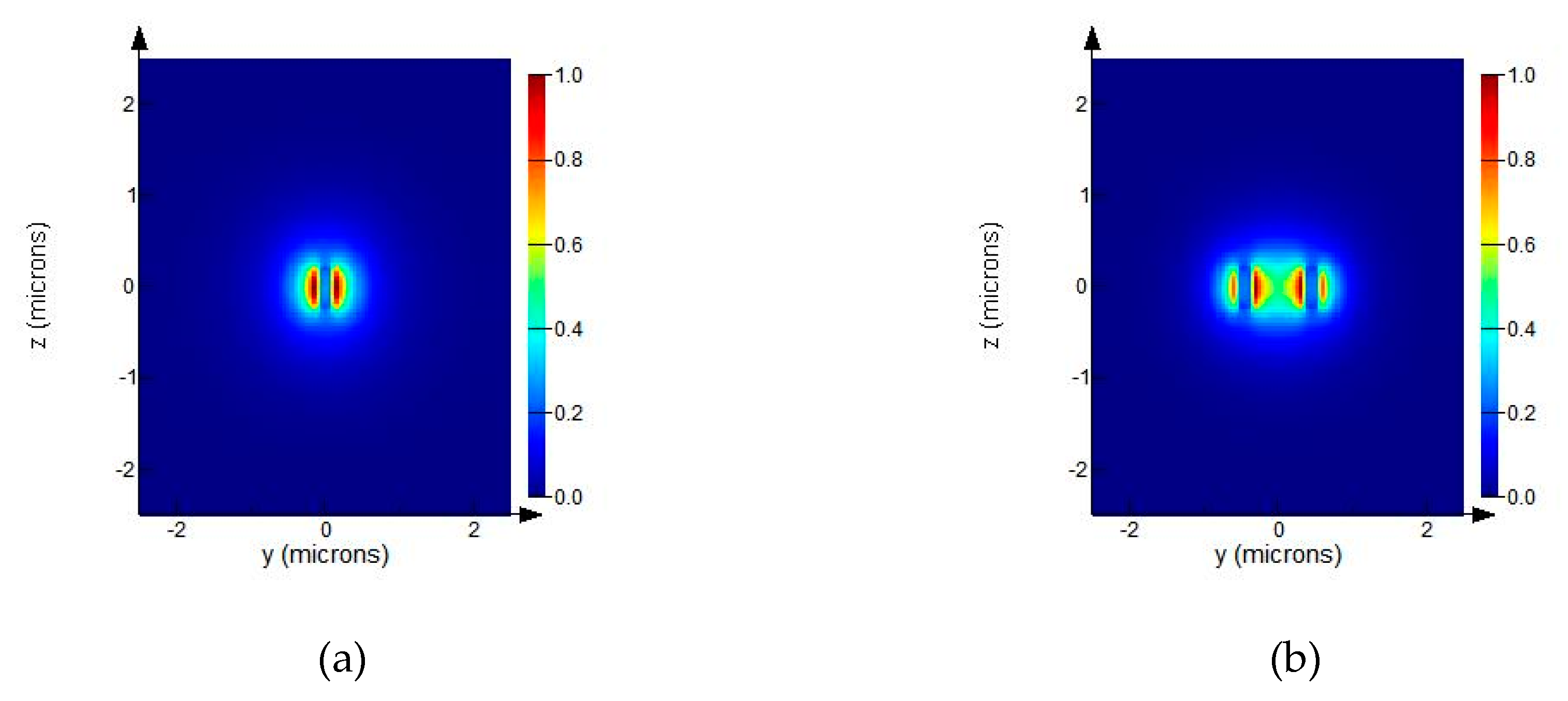
3.2. Edge Couplers Based on a Multi-Tip Taper

The coupling efficiency of a fiber-to-chip edge coupler can be simplified as the product of two factors: that is, the modal overlap between the fiber mode and the superimposed mode at edge coupler facet ( η 1 ) and the mode conversion efficiency of the edge coupler ( η 2 ). The definition of modal overlap efficiency η 1 can be expressed as
η 1 = | E 1 * E 2   dA | 2 | E 1 | 2 dA * | E 2 | 2 dA
where A is the modal distribution area, while E1 and E2 stand for the electric fields of the fiber mode and the superimposed mode at the coupler facet separately [55]. Since the total coupling efficiency of an edge coupler is determined by both η 1 and η 2 , it is intuitive to improve the overall coupling efficiency by increasing either η 1 , η 2 , or both of them.
The multi-tip taper is widely applied to improve the modal overlap efficiency [56,57,58], and the schematic of a multi-tip taper is presented in Figure 5a. A superimposed mode can be formed at the taper facet of the single taper, which consists of multiple tips, and the modal field diameter (MFD) is thus increased to better match with the fiber mode regarding the aspect of modal size. The design parameters of a multi-tip taper include the number of tips, interval distance between adjacent tips, taper tip width, and taper length, which can be properly designed to achieve high modal overlap in different situations, and the shape of the multi-tip taper may resemble a fork or a comb. In the case of fiber-to-chip coupling, the edge coupler facet should be aligned with the fiber core accurately to ensure fine overlap; thus, coupling efficiency is highly sensitive to alignment condition. Since it is a set of multiple tips as a whole that interconnects with the fiber, the dependence on misalignment and fabrication deviation reduces, considering each single tip in a multi-tip taper coupler. A multi-tip taper with multiple tips can loosen the constraints of alignment and reach larger misalignment tolerance as well as fabrication deviation tolerance.
The utilization of multiple tips can introduce a high degree of design freedom to realize the expected coupling efficiency within a notably small footprint. The total length of a multi-tip taper is usually below 100 μm [59,60]. As depicted in [60], an edge coupler on the basis of double-tip inverse tapers is designed, fabricated, and characterized. It reaches a low coupling efficiency of 1.1 dB for the TE mode and 1.52 dB for the TM mode respectively at 1550 nm within an ultra-compact size of 40 μm. A narrow slot is formed between two adjacent tapers, and the tip width of the slot is typically the feature size of the entire structure, at a value of several tens of nanometers. On this basis, a multi-tip taper is commonly prepared via electron beam lithography (EBL) patterning, which is highly precise and convenient with a single-step process at the expense of being time-consuming and expensive. In addition to general applications in fiber-to-chip optical coupling, multi-tip tapers with flexible tip width and tip numbers can also work under chip-to-chip communication [56] or laser-to-chip optical interconnect [59].

3.3. Edge Couplers Based on Multiple Tapers

Inspired by the idea of the multi-tip taper, it is natural to propose another kind of edge coupler based on multiple tapers. The trident edge coupler with three separate tapers is the most common form among different types of edge couplers consisting of multiple tapers [61,62,63,64,65], and its structure is presented in Figure 5b. For trident edge couplers, light exiting from the fiber firstly enters the facet composed by two bilateral taper tips and is split into a superimposed mode due to the high refractive index contrast between Si and SiO2 when light continues to propagate along the edge coupler. A central Si taper appears and the mode exists in all the three tapers, and the proportion of mode confined by the central taper tends to increase as the width of the central taper becomes larger. Finally, when bilateral tapers end, the mode is totally converted into the central taper and then propagates into successive integrated circuits. Figure 6 compares the modal distribution at the facet of edge couplers based on one taper and trident tapers. As mentioned in Section 3.1, an inverse taper is aligned with the fiber at the narrow end, and the mode distributes in the outer area of the taper, as shown in Figure 6a. In the trident edge coupler, light emitted from the fiber firstly propagates into the two bilateral tapers and exists as a superimposed mode, as presented in Figure 6b. Figure 6 clearly shows that when the other parameters are kept the same, an edge coupler based on multiple tapers has a larger modal area at the facet than that composed of one single taper. An enlarged modal distribution area can contribute to a higher modal overlap and reduce the modal size mismatch between the fiber and the chip facet.
An edge coupler composed of multiple tapers has a simple structure, high feasibility, and is compatible with traditional lithography and etch processes. Similar to edge couplers with one multi-tip taper, multiple tapers are also more tolerant to misalignment between an optical fiber and the edge coupler than a single inverse taper. Despite the advantages of low modal mismatch and a simple fabrication process, alignment between tapers within the edge coupler needs sophisticated design to prevent excess loss. Take a trident edge coupler for instance [64]; it is prepared by a 248 nm deep ultraviolet (DUV) lithography, and the total length is around 300 μm. It exhibits a coupling loss of 1.4 dB for the TE mode and 1.5 dB for the TM mode separately, with a loss variation below 0.1 dB over the C-band. Both polarization independence and wavelength insensitivity are revealed. However, the relative position between the bilateral tapers and the central taper has strong influences on the coupling performance. A slight deviation of 1 μm between the fiber and the trident coupler can introduce 1-dB excess loss. Researchers have applied different numbers and spatial locations of tapers to engineer the mode distribution and adjust the effective spot size to reduce modal mismatch. Moreover, there exists a trade-off between the number of multiple tapers and device performance as more tapers can provide a larger mode size while introducing higher propagation loss and a more complicated fabrication process. Despite general usage in fiber-to-chip optical interconnects, edge couplers based on multiple tapers can also operate as laser-to-chip couplers [63]. This particular application provides an approach to realize a hybrid integrated light source on photonic chips.

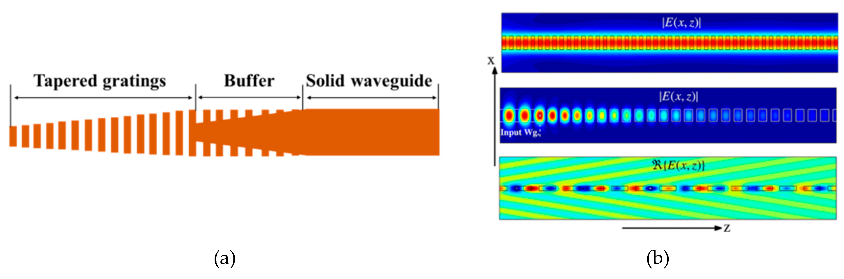
3.4. Edge Couplers Based on Subwavelength Gratings Structure

The concept of a subwavelength gratings structure (SWG) was proposed as an innovative concept in silicon photonic waveguide design more than one decade ago by researchers at the National Research Council of Canada [66] and has been widely adopted [67,68,69,70] due to its extraordinary characteristics in silicon photonic devices. The structure of a subwavelength grating is demonstrated in Figure 7a, where Λ stands for the grating pitch and B is the length of Si blocks. Subwavelength gratings refer to those gratings satisfying the relationship of pitch Λ and wavelength λ described as
Λ < λ 2 * N eff
where N eff is the effective refractive index of mode propagating inside the waveguide [71]. As shown in Figure 7b, when the grating pitch is much larger than the wavelength, light is blocked by the Si blocks, and radiation happens at the facet, which prevents further light propagation along the grating. Only a certain component of light that satisfies the Bragg condition can go through the grating structure, which acts as a conventional diffraction grating. In circumstances where the wavelength and grating pitch are comparable in length, reflection occurs. As for gratings with small pitches under the subwavelength regime, light can directly propagate through the grating, as it behaves in a general continuous Si waveguide.
Figure 8a shows a taper based on a subwavelength gratings structure, and it can be divided into three parts as notated in the figure: namely, a tapered gratings region, buffer region, and solid waveguide. In the region of tapered gratings that is aligned with the fiber, there is a high degree of design freedom to optimize the taper performance. Referring back to Equation (1), modal overlap η 1 is mainly dependent on the tip width and mode effective index at the front part of the tapered gratings, while the effective index is determined comprehensively by the tip width, pitch, and duty cycle of the grating. In other words, it is feasible to properly design geometry parameters in the tapered gratings region to engineer the effective index to match with the fiber mode maximally. Light can propagate through this pure subwavelength gratings region continuously, as depicted in the top subgraph of Figure 8b. It is followed by the buffer region, where the structure is a hybrid with both subwavelength gratings and the solid taper. With the aid of the Si solid taper, an effective index in the buffer region can gradually increase along the propagation direction due to the increasing proportion of the solid taper, and the mode confinement in the Si taper becomes gradually stronger. This subtle transformation of the structure effective index enables the mode to propagate at an ultra-low conversion loss and prohibits modal transition to higher-order modes, which consequently contributes to the high mode conversion efficiency η 2 and good adiabaticity. In contrast, a sharp change in the effective index without the buffer region can lead to significant reflection and scattering loss at the interface of the tapered gratings and the solid waveguide. Finally, there is a solid straight waveguide for the SWG taper connecting with the following circuits.
The above research works merely use one SWG-structured taper to function as an edge coupler [66,67,68,69,70]. However, it is intuitive to put forward a combination of subwavelength gratings structures with multi-tip tapers [72] and multiple tapers [73]. The structures of the multi-tip edge coupler and multi-taper coupler based on subwavelength gratings are shown in Figure 9a,b respectively. Introducing the subwavelength gratings structure can reach a lower effective modal refractive index than the Si waveguide at the coupler facet and achieve higher modal overlap with low-index fiber. Multiple variables in the SWG structure provide a high degree of design freedom; hence, it is possible to obtain excellent coupling performance including high coupling efficiency, compact size, low sensitivity to polarization status, and broad bandwidth. Take the fork-shape coupler and trident coupler shown below in Figure 9 [72,73] as an example; they both achieve an ultra-small footprint with a length of 36.5 μm and 35 μm respectively, which are much more compact than traditional edge couplers based on a single solid taper with a length around 300 μm or even longer. This remarkable merit of ultra-compact size makes SWG-assisted couplers suitable for application scenarios where dense integration is highly demanded. The presented SWG fork-shape coupler in Figure 9a achieves a low coupling loss of about 1 dB and an ultra-broad 0.5-dB bandwidth over 100 nm near the 1550 nm wavelength. Furthermore, it can be fabricated via one-step EBL, which is simple for fabrication. In fact, the fabrication process of a SWG structured edge coupler can be regarded as a synthetic procedure of conventional gratings and inverse tapers, which is feasible and compatible with the CMOS process. Additionally, the performance of an edge coupler based on subwavelength gratings can be further optimized if varied pitches and duty cycles are taken into consideration.

4. Structural Transformations of Edge Couplers in Vertical Direction

4.1. Edge Couplers Assisted with Multiple Upper Waveguides

Typical silicon photonic integrated circuits are based on the SOI platform, which is composed of a thick silicon substrate, buried silicon dioxide for isolation, a photonic circuits layer, and top silica cladding for protection from bottom to top. It has the potential to make some changes in the vertical dimension within the buried silicon dioxide and the top cladding to improve the device performance. As for the vertical structural transformation of fiber-to-chip edge couplers, the main aim is to enlarge the effective modal area in the vertical direction to achieve a high modal match between the fiber core and the coupler facet. Figure 10 shows an approach to obtain a large effective modal area where multiple waveguides are placed above the Si inverse taper [74,75]. Upper assisting waveguides are usually made of materials with a lower refractive index than silicon such as silicon nitride (SiN) and silicon oxynitride (SiON), which are also well compatible with the typical silicon photonic platform and CMOS fabrication process. Figure 10 demonstrates one type of pattern under which assisting multiple waveguides are introduced [76]. In principle, assisting waveguides should be placed above the appearance of an inverse taper so that the propagating mode distributed outside the narrow taper can be transmitted and confined upwards. Due to the existence of upper assisting waveguides with higher refractive indexes than the surrounding silicon dioxide cladding, light tends to be confined into the multiple assisting waveguides. Therefore, the lower Si inverse taper together with the upper assisting waveguides support a superimposed mode, and the modal area becomes enlarged and is comparable to that of the fiber core, which helps efficiently couple the light emitting from the fiber.
Technically, it is possible to manipulate the ultimate modal distribution by changing the quantity, material refractive index, and orientation of the assisting waveguides, and Voigt et al. have discussed the performance of assisting waveguides with different patterns [76]. Taking fabrication issues into consideration, it is feasible to fabricate the multiple SiN or SiON waveguides since they are well compatible with the silicon photonic fabrication process. Nevertheless, alignment should be taken care of to reach the expected performance, and alignment marks need to be carefully designed during the deposition of each layer. Generally, there are several situations under which alignment issues should be considered. Firstly, upper assisting waveguides are required to align with the Si inverse taper laterally to ensure proper modal distribution and conversion. Next, as assisting waveguides are located at various heights (or different layers), interlayer alignment should be achieved to obtain the required waveguide pattern. Lastly, a superimposed mode is formed within the Si inverse tape; thus, the assisting waveguides should also be deposited and aligned longitudinally above the taper part to promote upward modal transition.
Specifically, a novel spot size converter assisted with multiple upper SiON waveguides for coupling with standard SMF is demonstrated in [75]. Simulations are comprehensively run including detailed discussion about fiber alignment tolerance, robustness to fabrication tolerances, and compatibility with standard microfabrication processes. This spot size converter can achieve a nominal low loss of 0.4 dB with a total length of 450 μm. A 1-dB excess alignment tolerance with SMF is larger than 2 μm while a 3-dB excess alignment tolerance is nearly 4 μm. This novel design reduces the complexity of alignment and fixation of a SMF to photonics chips, but it is quite challenging for fabrication feasibility and further practical applications.

4.2. Edge Couplers Based on Cascaded Multi-Stage Tapers

The last section shows the structural transformation of edge couplers in the vertical direction via assisting waveguides grown above the silicon inverse taper with an isolation layer of SiO2. Accordingly, it is also feasible to achieve a vertical transition of the propagating mode via cascaded tapers, as presented in Figure 11. An edge coupler based on multi-stage tapers consists of multiple unidirectional tapers in different layers with their wide end near the fiber and narrow end close to successive photonic waveguides. At the wide end where tapers in different layers merge, the edge coupler has a large cross-section area which is comparable with the fiber core, and light can couple into the coupler facet at a relatively low discrepancy. In the region of multi-stage tapers, the taper at the top layer has the shortest length, while the one at the bottom layer has the longest length. When light propagates in the cascaded multi-stage tapers and arrives at the first taper tip where the top-layer taper ends, light cannot be confined well in the top layer due to a too small cross-section area, and it inclines to transmit into the successive layer below, which has a higher refractive index than the surrounding SiO2 cladding. Likewise, light propagates in the second layer taper for a certain distance and then continues to transmit downwards when it propagates to the second taper tip until it reaches the bottom layer.
Considering the material of each layer, it can be silicon, silicon oxide, silicon nitride, or other kinds of polymers that have proper refractive index and compatibility. Edge couplers based on cascaded multi-stage tapers can be divided into two main types according to the mechanism following, in which the bottom layer connects with the silicon waveguides. Under the first type illustrated in Figure 11a, the silicon taper acts as the bottom layer, and it is cascaded with upper layers in the same direction with the wide end near the fiber and narrow end connected with photonic circuits [77,78,79]. In each layer, light firstly exists as a fully supporting mode, and as it propagates to the narrow taper end, the mode is transited into the lower layer, which is longer in size. After all, the mode can be transmitted into the bottom Si device layer; then, it propagates within the following photonic circuits. As for the second type shown in Figure 11b, an inverse silicon taper is buried in the bottom stage to enable mode conversion [80,81,82]. The structure and mechanism of the upper stages are the same in both regimes; however, in the type of cascaded multi-stage tapers above an inverse taper, the bottom stage is different regarding its cuboid shape, which acts as an equivalent cladding in fact. One key design principle is that the bottom stage should have a lower refractive index than silicon, so that the mode can convert into the buried silicon inverse taper and then the silicon photonic waveguides.
Figure 12 presents the modal distribution in a cascaded multi-stage mode converter under the regime where an inverse silicon taper is buried in the bottom stage [82]. There are three SiO2 stages in this configuration, and the yellow taper-shape envelope stands for the first stage, while the blue taper-shape envelope stands for the last stage. In the right part of Figure 12, it shows that the optical field is transmitted downwards between each layer. This fiber-to-waveguide mode converter exhibits a low loss of 1.5 dB and a broad 1-dB bandwidth that is more than 100 nm within a total length of about 200 μm. Assisted with the multi-stage upper waveguides, this coupler can couple directly with the SMF near the 1550 nm operation wavelength. Multiple (more than five) lithography and etch processes are adopted to form the Si and SiO2 tapers, and chemical mechanical polishing (CMP) is applied before the deposition of each stage. Alignment tolerance with a fiber is also measured in this design, with 2.5 μm and 2 μm for 1-dB excess in horizontal and vertical directions, separately.
The quantity of stages in the cascaded multi-stage edge coupler is unconstrained, but it should be proper, since too many layers will increase the fabrication complexity with excessive steps of deposition and lithography, while too few layers may lead to insufficient mode conversion into the critical silicon layer. Generally, three to five layers are most commonly used for cascaded multi-stage edge couplers. The complexity of the fabrication process is determined by how many stages are utilized, since lithography, etch, and polishing are required to prepare the taper structure in each layer. In addition, the sidewall roughness of the taper in each layer can also lead to excess loss to coupling efficiency [83,84,85,86,87]. Interlayer taper tip alignment should be considered, and thick cladding needs to grow upon the traditional SOI structure to reduce the mode size mismatch with the fiber core. To summarize, the fabrication of a multi-stage edge coupler is compatible with the typical CMOS process, and the main processes include optical lithography, etching, deposition, and polishing. However, the fabrication can be very complicated and time-consuming due to the existence of multiple stages, which constrains the practicality and feasibility of wide application. In research scenarios where a single mode fiber is used, this kind of configuration is quite suitable because of its large spot size, low modal mismatch, and high alignment tolerance. However, its path toward commercialization is blocked.

4.3. Edge Couplers with Index-Matching Cladding

Apart from edge couplers based on cascaded multi-stage tapers, there are also some research works about edge couplers with a Si inverse taper buried in index-matching claddings [88,89,90,91,92,93,94,95]. The typical structure of an edge coupler assisted with index-matching cladding is presented in Figure 13, and we can observe that unlike the Si layer underneath the SiO2 cladding, other kinds of materials including SiN, SiON, and polymers are utilized to engineer the refractive index between the value of the fiber core and silicon waveguides. In some cases, there may be an additional intermediate layer between the silicon waveguides and the top index-matching cladding. Lee et al. applied the combination of two types of polymers—that is, WIR30-490 with a higher index as the top cladding and ZPU450 with a lower index as the secondary waveguide connected with a silicon taper [88]. Pu et al. decreased the thickness of the SiO2 cladding and designed a thick polymer waveguide as its top cladding [89]. Bakir et al. had an adjustment on the basis of typical silicon dioxide and substituted it with silicon-rich oxide with a higher refractive index of around 1.6 [90]. Raghunathan et al. applied initiated chemical vapor deposition to form the polymer cladding on top of the amorphous silicon core [91]. Ku et al. designed a structure composed of both the SU-8 three-dimensional taper and the silicon oxynitride intermediate. SiON was deposited surrounding silicon waveguide and could transmit light gradually from the SU-8 3D taper to the bottom silicon layer [92]. Jia et al. used an intermedium layer made of SiON that surrounded the Si core and was surrounded by a Si O 2 top cladding. In this structure, the SiON intermediate layer can be regarded as a secondary core encircling the Si waveguide [93]. Takei et al. had a similar design with Jia’s work in [93] with SiON as the transition material as well as the secondary core in the coupler [94]. Maegami et al. designed a SiO2 spacer to isolate the Si taper and SiON layer, and the Si taper is knife-shaped with slanted sidewalls [95].
In [89], due to the narrow tip width of the Si inverse taper (approximately 40 nm), EBL is applied to form the Si taper on the SOI wafer, and thermal oxidation is applied to grow a thin layer with 30 nm thickness of SiO2 on the Si taper. A top cladding of SU8 polymer is spin-coated on the thin SiO2 layer and then patterned with EBL. The thickness composition of the Si, SiO2, and SU-8 layer is delicately optimized to make the effective index in the mode converter close to that of the coupling fiber. The extraordinary coupling performance of the TM mode is achieved at an ultra-low loss about 0.36 dB within a 300 μm-long footprint. An additional 3-dB loss for 1.5 μm misalignment in both the vertical and horizontal directions is measured. It is straightforward to increase the modal overlap between the fiber core and the photonic circuits regarding aspects of both size and effective index with the aid of the refractive index matching a cladding of proper thickness. The fabrication process of the index matching layer is simpler than that of the edge couplers with multiple assisting waveguides and multi-stage tapers mentioned in previous sections. One prerequisite is to determine appropriate kinds of index matching material or to synthesize a specific type of material according to the requirements of the refractive index value. Theoretically, the refractive index of the matching cladding should be close to that of the fiber core to decrease the index mismatch. The selection of optical lithography or electron beam lithography depends on the feature size in the entire configuration, which is commonly the taper tip width. Taking the utilization of only one single taper and its narrow tip width into consideration, the spot size is usually much smaller (approximately 3 μm) than that of the standard SMF. Thus, edge couplers with index-matching cladding are particularly feasible for coupling with lensed fibers or high-numerical-aperture (HNA) fibers whose spot size is also compressed.

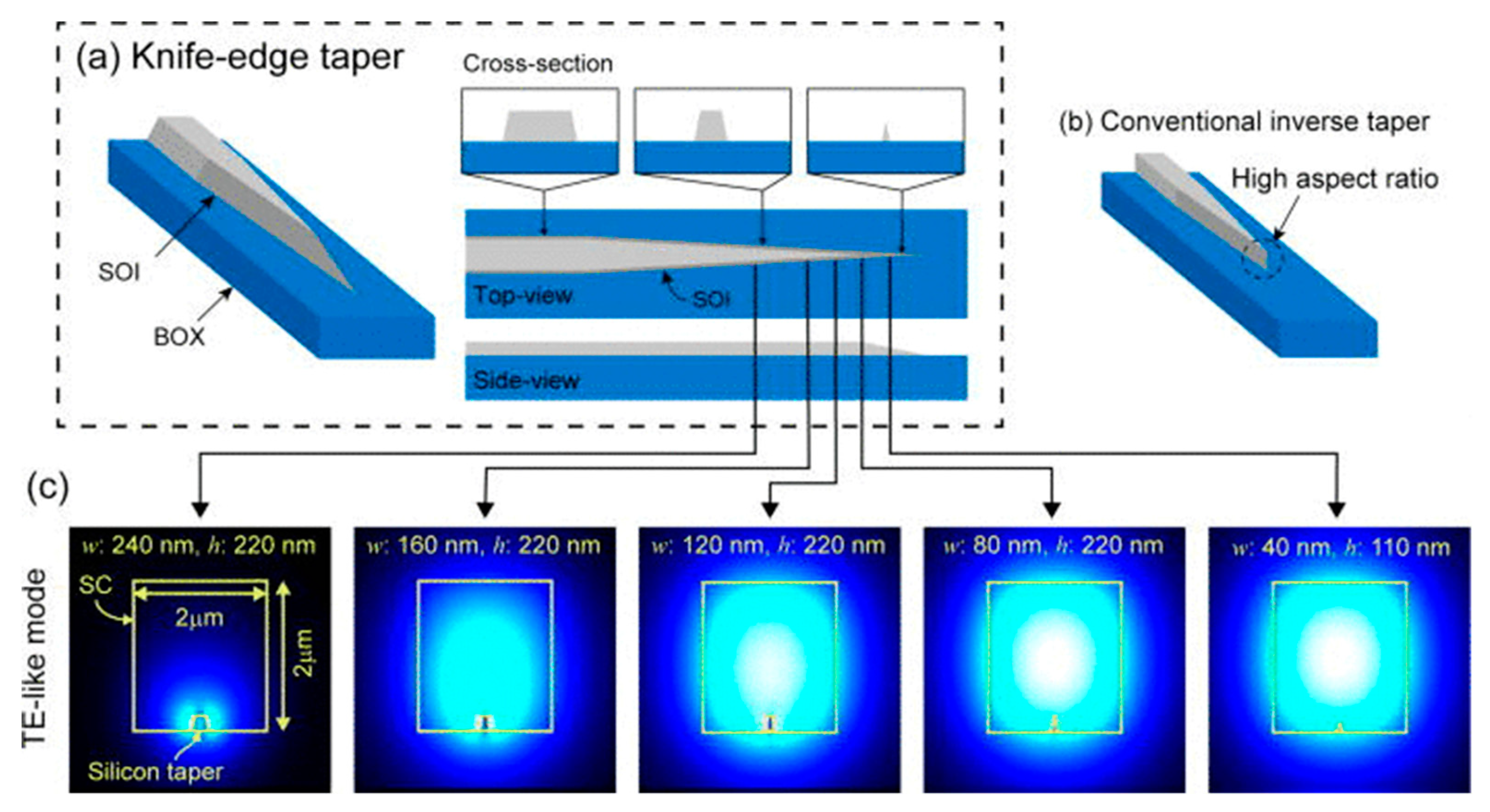
4.4. Edge Couplers Based on Three-Dimensional Taper

Typical tapers only have tapering profiles in the longitudinal and lateral dimension, while the thickness of the taper stays constant. However, it is possible to transmit light from the fiber through a three-dimensional taper (3D taper) that can gradually converge. As shown in Figure 14a, a 3D taper is aligned to fiber with its wide end, which is comparable with the fiber core in the aspect of structure size. Then, it begins to taper in both the vertical and horizontal dimensions to connect with the silicon waveguide. Generally, three-dimensional tapers can be divided into two main types: one is purely silicon-based 3D tapers, and the other is 3D tapers assisted with other kinds of intermedium materials. As for the purely silicon-based 3D tapers [96,97,98,99], there are also two different approaches to adjust the three-dimensional profile. In some previous works [96,99], the wide end of the taper becomes narrower in both the vertical and lateral directions until it forms a narrow end with the same thickness and width as the silicon waveguide as presented in Figure 14b. In some other works [97,98], the 3D taper firstly begins to reduce in thickness while the width remains unchanged. Then, the 3D taper transits into a thin silicon slab with the same thickness as the silicon waveguide, and then the lateral slab gradually tapers similar to a traditional two-dimensional taper, which connects with the silicon waveguide afterwards, as shown in Figure 14c.
There are also some 3D tapers assisted with other materials to match with the fiber core considering both the size and the effective index as Figure 14d depicts. Amorphous silicon [100,101], SU-8 [92,102], SiON [92], and other kinds of index-matching materials are applied in such situations. These materials are compatible with silicon photonic platform and have a moderate refractive index between silicon dioxide and silicon, which can help improve the modal match between the fiber and the waveguide. Figure 15a demonstrates a type of knife-edge 3D taper coupler following the regime depicted in Figure 14b. Compared with conventional inverse taper in Figure 15b, its taper tip is specially designed with a low aspect ratio. The i-line stepper is used for patterning and the silicon taper is prepared with inductive-coupler-plasma reactive ion etching (ICP-RIE) to form the slanted sidewall. Then, dry-etching is performed in CF4 atmosphere. A secondary core made of benzocyclobutene is introduced to engineer the refractive index as well as to protect the functional Si waveguide from the exposure of CF4 during etching. The narrow knife-edge shape tip is aligned with the fiber in practical measurement. As for the TE mode conversion presented in Figure 15c, it is clear that the confinement of mode is increasingly stronger when light propagates inside the taper. The TE mode conversion loss is 0.35 dB for this configuration, and the device size is 180 μm. The bandwidth feature and fabrication tolerance are not given out in this research work.
Although it is easy to think of connecting a large fiber core with a 3D taper, three-dimensional tapers are not easy, considering the fabrication process. Among the research works mentioned above, various fabrication techniques are utilized to make a 3D taper, including gray-tone optical lithography [96], KOH wet etching for slanted surfaces [97], shadow mask [100], annealing in hydrogen ambient [101], etc. These fabrication processes are difficult to operate and control to some extent, and thus, they limit the adaptability and practicality of the three-dimensional tapers. In other words, the design of ideal 3D tapers is indeed a matter of fabrication techniques. It is necessary to control the reaction speed and reactant dose accurately and precisely to reach the desired vertical taper slope and to avoid the thick wedge from collapsing. The challenges and difficulties in fabrication underlie the reduced feasibility and ability to integrate 3D taper edge couplers.

4.5. Edge Couplers Based on Cantilever Structure

Several forms of vertical transformation of edge couplers have been depicted in previous sections including couplers assisted with multiple waveguides, couplers based on cascaded multi-stage tapers, couplers with index-matching cladding, and couplers based on three-dimensional tapers. Basically, these edge couplers have additionally designed structures upon the Si inverse taper. Typical SOI wafers use thick silicon as the substrate and grow a layer of silicon dioxide with a thickness of several microns as the buried oxide layer to isolate the device layer with the substrate. Intuitively, it is also applicable to design specific structures below the Si inverse taper. Cantilevers structures are commonly used in micro-electro-mechanical systems (MEMS), and they also play important roles in edge coupler design [103,104,105,106,107]. The schematic of such a structure is demonstrated in Figure 16. Based on initial single Si inverse taper, the BOX layer and the substrate underneath the BOX layer are partly undercut to a certain thickness, and a suspended beam of Si taper cladded with SiO2 is exposed. Several supporting beams are set to sustain the suspended arm to enable structure stability. A fiber is placed in the etched slot and aligned with the cleaved facet of the cantilever arm.
Detailed process flow can be found in [103]. The converter is composed of suspended SiO2 waveguide and overlapped Si taper. This novel design reaches approximately 2.0 dB coupling loss with a 5 μm-MFD lensed fiber in the wide wavelength range from 1520 to 1600 nm. The 1-dB excess loss for alignment tolerance is about 1.7 μm. The device has a rather large footprint with 550 μm length. Overall, this cantilever edge coupler achieves fair coupling performance at the expense of too long size. More importantly, the complexity and difficulty of the fabrication process make this configuration less competitive when compared with other couplers that can achieve comparable performance under much easier fabrication. Nonetheless, the cantilever structure is a novel and clever design, actually. From one aspect, the undercut slot that remains after etching can further isolate the functional structure away from the Si substrate, which has a high refractive index, and mode leakage into the Si substrate can be significantly reduced. In some cases, refractive index-matching oil is filled in the slot below the suspended arm to further decrease the index mismatch between the fiber and the coupler [31]. From the other aspect, the remained cantilever arm has a similar formation with fiber [104]; namely, the suspended arm itself acts as an equivalent core, and the encircled intermediate in the etched slot acts as an equivalent cladding. This similarity in structure composition helps efficient coupling.
The main obstacle to design a cantilever edge coupler is the complicated fabrication processes, since it is quite challenging to fabricate the cantilever structure. Multiple steps of lithography and etch are required to obtain the cantilever arm and deep trenches sequentially. In addition, pattern masks should be precisely designed and adjusted to control the dimension of the cantilever arm. These constraints make it hard for cantilever edge couplers involved in mass production. However, the delicate structure of cantilever edge couplers can help exploit higher device performance in research scenarios. It also has the potential to integrate cantilever edge couplers with the aforementioned MEMS, which may inspire novel photonic devices and integrated systems. In summary, it is intuitive to find that for edge coupler configurations with vertical transformations, the fabrication process is commonly more complicated and infeasible than those configurations with horizontal transformations. Monolithically fabrication processes are more compatible with planar photonic integrated circuits. In addition, excess manufacture of either the Si substrate or the cladding of the standard SOI wafer will bring about high cost and inferior integrability.

5. Discussions and Perspectives

5.1. An Overall Overview of Edge Coupler Performance

The different types of structural transformations of fiber-to-chip edge couplers mentioned in previous sections have been reorganized in Table 1 for convenience of reference and comparison. Table 1 reveals that edge couplers can realize very high coupling efficiency up to 90%, and the device footprint is usually of several hundred microns. Edge couplers generally perform stably in a broad operation wavelength bandwidth, and relatively low polarization dependence for TE and TM modes is shown.
Due to the low coupling losses of single-edge couplers, a cut-back method is usually applied in the testing of edge couplers to measure the coupling efficiency [26,68,108] assisted with multiple auxiliary sets of ultra-long straight waveguides and bends to acquire accurate experimental results. In some situations, fiber array can be customized to place at one facet or both facets to ease the alignment issue. Since edge couplers work for butt coupling, the quality of chip facet is critical in practical experiments and applications. There are two main factors to take care of in the preparation of chip facet. Firstly, there should be a proper spacing between the chip facet and the coupler facet to protect the device structure as well as reduce power evanescence when light propagates within the under-confined spacing. Typically, a spacing of several microns to several tens of microns is acceptable, and refractive index-matching oil can be used for more precise refractive index management. Secondly, the surface roughness of the chip facet should be as low as possible to prohibit excess light reflection and scattering. The facet can be prepared via firstly deep reaction ion etching and then laser dicing or mechanical dicing to obtain a smooth sidewall with low surface roughness even to the order of several hundred nanometers.

5.2. A Brief Comparison between Edge Couplers and Vertical Couplers

As mentioned previously in the Introduction, under the vertical coupling regime, fiber is placed above certain coupling structures (mostly diffractive gratings) on the top of planar photonic chip. A vertical grating coupler changes the off-plane wave-vector direction of light to the in-plane waveguide direction via grating structures with either periodic or chirped pitches, and it couples the light into on-chip waveguide via a spot-size converter. The wave-vector conversion can be described by the Bragg condition, which relates the pitch of grating, structure effective index, and beam incident angle with a certain wavelength that satisfies the condition [34]. Grating couplers are advantageous considering their compatibility to wafer-level testing, flexibility for aligning and measurement, and relatively compact size [109,110]. However, it is also important to figure out some drawbacks of grating couplers. Firstly, the coupling efficiency is rather low due to the inherent diffraction and scattering that occurs in the grating structure. The component of light that does not satisfy the phase match condition is eliminated during propagation inside the grating. Secondly, also owing to the phase match condition, only light within a particular wavelength range can travel through the grating. This property leads to the limited narrow bandwidth of grating couplers. Thirdly, the teeth of the grating structure have high directionality, which is very sensitive to the oscillation direction of the electromagnetic vector. This presents as the TE or TM polarization status from the macro perspective. Thus, the wave-vector conversion has the underlying drawback of polarization sensitivity for grating couplers.
High-efficiency grating couplers have been also reported, but they usually include complex fabrication processes such as a bottom mirror below the grating or silicon overlay layer above the grating [111,112,113]. To deal with wavelength sensitivity and polarization sensitivity issues, polarization splitting grating couplers and dual-wavelength-band grating couplers are proposed [114,115]. In the meantime, these designs usually bring increased coupling loss. When it comes to edge couplers, despite the apparent advantages such as high coupling efficiency, broad bandwidth, and low dependence on polarization, the main limits lie in that edge coupling only allows the alignment of fiber with the coupler at the chip facet, which is less convenient compared with grating couplers that support wafer-level testing at different positions on the wafer plane [116,117,118]. Meanwhile, edge couplers generally have larger footprints in the longitudinal dimension. In addition, the particular designs of edge couplers with the aforementioned cascaded multi-stage tapers, 3D tapers, or cantilever structure need complex and difficult fabrication processes. The performance of typical vertical grating couplers and edge couplers are summarized and shown in Table 2 for quick comparison.

5.3. Packaging Issue of Optical Couplers

Optical interconnects are necessary for photonic integrated circuits working as a component in an optical fiber network. For a photonic chip design from proof of concept to commercial prototype, packaging and assembly is a crucial point and may be one of the most significant bottlenecks on the way to commercialization [119]. It is essential to provide an interface for packaged photonic integrated circuits to connect with fibers in the fiber-to-chip coupling regime. Corresponding to the aforementioned coupling strategies, there are generally two types of fiber-to-chip coupling in packaging, namely edge coupling and grating coupling. Lateral coupling is appropriate for planar photonic integrated chips, but it is challenging for lateral edge coupler to provide a desirable alignment [120]. Vertical coupling with grating couplers are mainly adopted since fibers can be placed at multiple positions on the chip to connect with grating couplers.
The packaging of photonic chips has high demand in the aspects of alignment precision, thermal management, and the feasibility of integrating active and passive devices together. Coupling efficiency is the most important figure of merit in packaging and bandwidth, and polarization dependence should also be taken into consideration. Edge coupling can reach high coupling efficiency, broad bandwidth, and low sensitivity to polarization. However, the key limit of edge couplers is that it can only support optical coupling at the chip facet with no flexibility. There are two major drawbacks of packaging with edge coupling—that is, low misalignment tolerance and complicated fabrication processes. Firstly, at the 1550-nm wavelength, which is widely used in telecommunications, the typical 1-dB alignment tolerance of a single mode fiber is about 1.75 μm [39]. Since the modal field diameter of edge couplers is comparable to this value, a small deviation in the aligning fiber with the edge coupler facet can bring about a sharp decrease in coupling efficiency. Secondly, the packaging of edge coupling usually applies optical fiber pigtailing combined with laser welding [121]. The fiber requires cleaving, dicing, and tapering to lensed fiber in some cases. In addition, the chip facet needs delicate polishing to reduce the facet surface roughness and improve the coupling efficiency. An anti-reflection coating should be introduced further after the polishing process sometimes. These disadvantages make edge-coupling insufficient to be utilized in mass production at low cost.
Grating couplers dominate in fiber-to-chip packaging in most cases. From the industrial point of view, non-contact probing and the testing of packaged circuits is critical for flexible measurement and tests at low cost. Grating couplers have much larger mode spot sizes than edge couplers, which is suitable for coupling with SMF [121]. It is worthwhile to mention that edge coupling can suit for some particular photonic applications, including scenarios requiring high power transmission such as nonlinear silicon photonics and situations where broad bandwidth is needed to enable integrated devices with high optical input/output (I/O) counts and high-frequency characteristics [39]. As for the developing tendency of packaging with edge coupling, it is feasible to use HNA fibers to improve the coupling performance and loosen the alignment constraints. V-grooves are also used to passively place and align the fiber. However, a V-groove may occupy too large an area of the chip, impacting the integration density and cost. In addition, since the misalignment tolerance of edge couplers is comparable with the fabrication tolerance of fiber arrays, edge coupling is only applicable for single-channel packaging. Thus, it is extremely expensive and time-consuming when multiple fibers need to be connected; some research groups and companies also aim at developing multi-channel edge coupling under the benefit of its potential high coupling efficiency [119].

5.4. Future Trends of Silicon Photonic Edge Couplers

5.4.1. Polarization and Mode (de)Multiplexing Technology

It is easy to observe from Table 1 that the TE mode mostly performs better than the TM mode for a designated edge coupler, and nearly all related research works focus on the propagation and conversion of fundamental modes. As the high data transmission rate and large link capacity requirements increase, the tendency is to multiplex different polarization states and mode orders to carry more information in one particular device. Many studies have been conducted to design devices with low polarization-dependent-loss (PDL), and there are various approaches to improve the polarization insensitivity of edge couplers. For example, edge couplers with a square cross-section or based on multi-tip tapers have a square or enlarged effective cross-section area that can hold both TE and TM modes [28,122]. Subwavelength gratings structures can be utilized to engineer effective refractive indexes, and it is feasible to realize the equal modal effective indexes of TE and TM modes with proper parameters [123]. Polarization (de)multiplexers can also be used in combination with conventional edge couplers to multiplex different polarization status and reduce polarization dependence [124]. Moreover, techniques of polarization manipulation and management are summarized in [125,126]. As for mode multiplexing technology, broadening the taper width can support the existence of high-order modes [127], and a variety of mode (de)multiplexers have been proposed based on polarization splitters, directional couplers, and arrayed waveguide gratings [128,129,130,131,132].

5.4.2. Multilayer Silicon Nitride-on-Silicon Photonic Integrated Platform

To improve the integration density of silicon photonic integrated circuits, recent developments have shown increasing interest in the gradual emergence of multilayer integrated photonic platforms and multilayer silicon nitride-on-silicon integrated platforms in particular. Silicon nitride is a promising candidate in silicon photonic platforms due to its many advantages. Firstly, SiN is well compatible with the fabrication process of silicon photonics, which can be grown via low-pressure chemical vapor deposition (LPCVD) at high temperature (>700 °C) or plasma-enhanced chemical vapor deposition (PECVD) at low temperature (<400 °C) [133]. Secondly, silicon nitride waveguides have a lower refractive index (around 2.0 at 1550 nm) than that of silicon [134]. The relatively low index contrast with silica brings less light confinement and thus a larger waveguide dimension, making it less sensitive to sidewall roughness. Thus, the SiN waveguide has a lower propagation loss in the O-band than Si waveguide [133]. Although N-H and Si-H bonds absorption exists in the C-band, it can be avoided by choosing LPCVD instead of PECVD. Thirdly, SiN can support high optical power and is less sensitive to thermal change compared with Si, which means that it is possible to integrate active devices into a silicon photonic platform with the aid of SiN [108].
In cases of fiber-to-chip edge couplers, SiN waveguides have two major advantages over Si waveguides. Firstly, a SiN waveguide has a lower refractive index mismatch with fiber core than silicon, which can be designed properly to reduce the modal discrepancy with the fiber core and thus improve the modal overlap for fiber-to-chip coupling [135]. Secondly, the insertion loss can be reduced when assisted with multiple upper SiN waveguides, as described previously in Section 4.1. In addition, for vertical coupling, SiN allows a tri-level polarization independent grating coupler [134] and increases the coupling efficiency when silicon is served as a bottom mirror [136]. There are several leading research groups focusing on the multilayer silicon nitride-on-silicon platform, including Poon et al. from the University of Toronto [134,137,138], Lo et al. from the Institute of Microelectronics, Singapore [139,140], Bowers et al. from the University of California, Santa Barbara [141,142], etc. Some related research works of SiN couplers are demonstrated in Table 3, with comparison to photonic couplers in the SOI platform. Apart from the SiN-on-Si platform, there are also some research works on multilayer integrated photonic circuits with a combination of crystalline silicon and amorphous silicon [62,94]. The multilayer integrated photonic platform is a prospective trend for high link capacity and data transmission.

5.4.3. Inverse Design Method for Nanophotonics

The use of electronic design automation (EDA) software to assist electronic integration circuit design is both appropriate and has signaled an advance. Since photonic circuits are often analogized with electronic circuits, it is natural to come up with the idea of photonics design automation. All the design techniques mentioned in the previous sections are forward approaches that obey the logic following which a prototype of an edge coupler is proposed, and then its performance is evaluated via numerical simulation and experimental measurements. Recently, researchers have begun to use computer-aid design methods to exploit the performance advancement of edge couplers. Contrary to traditional forward design, performance metrics are firstly put forward, and then device structures are obtained by numerical calculation accordingly; thus, this is called inverse design. Jelena et al. from Stanford University have firstly proposed the concept of the objective-first inverse design method applied for photonics design in 2007 [143] and after that, increasingly more groups have caught up to focus on the inverse design method [144,145,146,147,148,149,150,151,152,153]. The inverse design procedure acts similar to a black box in which the input is the desired performance and the output is a certain structure. An arbitrarily initial structure is chosen, and specific requirements of performance are set such as a given coupling efficiency for an edge coupler; then, calculation and iteration will start under predefined optimization algorithms. In each iteration, a temporary intermediate structure is obtained, and the algorithm will determine whether this structure satisfies the predefined shutoff criterion. If the criterion is met, a final structure is achieved, and its performance will be evaluated regarding whether it has met the performance requirements. If the criterion is not satisfied, the design procedure will loop back to reach out a new intermediate structure, and the iteration goes on. The output performance will be compared with the predefined criterion at the end of each iteration step, and it will continue to be optimized on the basis of the existing structure. Consequently, the optimal result can always be achieved as long as enough iterations are run. The inverse design can closely approach the internal performance limits of silicon photonic devices.

6. Conclusions

Research works in recent years have witnessed the significance and practicality of silicon photonics in the field of photonic integrated chips. Optical interconnects in silicon photonic integrated circuits is a critical issue to focus on to achieve efficient data transmission. The two mainstream paradigms of fiber-to-chip optical interconnects, namely vertical coupling and edge coupling, have different characteristics, while edge coupling is superior in the aspects of higher coupling efficiency, broader operation bandwidth, and lower dependence on polarization status. This review firstly goes through the research background and applications of silicon photonic fiber-to-chip couplers. The operation mechanism and design principles are illustrated, and then the overall performance metrics of edge couplers are summarized. Furthermore, the structural transformations of edge couplers in the horizontal and vertical dimensions are classified and described in detail. In addition, we make a brief comparison between grating couplers and edge couplers and overview the packaging issues in optical coupling. Lastly, we discuss some of the experimental issues and potential perspectives regarding edge couplers, including polarization manipulation, the multilayer integrated photonic platform, and the inverse design method. It is convincing that silicon photonic edge couplers will be increasingly widely used and contribute to more improvements in the field of silicon photonic integrated circuits.

Author Contributions

Conceptualization, All Authors; Investigation, X.M., S.W. and L.C.; Original Draft Preparation, X.M.; Review and Editing, All Authors; Supervision, H.Y.F.; Project Administration, H.Y.F.; Funding Acquisition, H.Y.F. All authors have read and agreed to the published version of the manuscript.

Funding

This research is funded by the Shenzhen Science and Technology Innovation Commission (Project: JCYJ20180507183815699, JCYJ20170818094001391,KQJSCX20170727163424873), Tsinghua-Berkeley Shenzhen Institute (TBSI) Faculty Start-up Fund, and Shenzhen Data Science and Information Technology Engineering Laboratory.

Conflicts of Interest

The authors declare no conflict of interest.

References

  1. Jalali, B.; Fathpour, S. Silicon photonics. J. Lightwave Technol. 2006, 24, 4600–4615. [Google Scholar] [CrossRef]
  2. Soref, R. The past, present, and future of silicon photonics. IEEE J. Sel. Top. Quant. 2006, 12, 1678–1687. [Google Scholar] [CrossRef]
  3. Xu, D.X.; Schimid, J.H.; Reed, G.T.; Mashanovich, G.Z.; Thomson, D.J.; Nedeljkovic, M.; Chen, X.; Thourhout, D.V.; Keyvaninia, S.; Selvaraja, S.K. Silicon photonic integration platform—Have we found the sweet spot? IEEE J. Sel. Top. Quant. 2014, 20, 189–205. [Google Scholar]
  4. Thomson, D.; Zilkie, A.; Bowers, J.E.; Komljenovic, T.; Reed, G.T.; Vivien, L.; Marris-Morini, D.; Cassan, E.; Virot, L.; Fédéli, J.-M.; et al. Roadmap on silicon photonics. J. Opt. 2016, 18, 073003. [Google Scholar] [CrossRef]
  5. Chen, X.; Milosevic, M.M.; Stankovic, S.; Reynolds, S.; Bucio, T.D.; Li, K.; Thomson, D.J.; Gardes, F.; Reed, G.T. The emergence of silicon photonics as a flexible technology platform. Proc. IEEE 2018, 106, 2101–2116. [Google Scholar] [CrossRef] [Green Version]
  6. Xiao, X.; Li, Z.; Chu, T.; Xu, H.; Li, X.; Nemkova, A.; Kang, X.; Yu, Y.; Yu, J. Development of silicon photonic devices for optical interconnects. Sci. China Technol. Sci. 2013, 56, 586–593. [Google Scholar] [CrossRef]
  7. Chen, X.; Li, C.; Tsang, H.K. Device engineering for silicon photonics. NPG Asia Mater. 2011, 3, 34–40. [Google Scholar] [CrossRef] [Green Version]
  8. Subbaraman, H.; Xu, X.; Hosseini, A.; Zhang, X.; Zhang, Y.; Kwong, D.; Chen, R.T. Recent advances in silicon-based passive and active optical interconnects. Opt. Express 2015, 23, 2487–2510. [Google Scholar] [CrossRef] [Green Version]
  9. Son, G.; Han, S.; Park, J.; Kwon, K.; Yu, K. High-efficiency broadband light coupling between optical fibers and photonic integrated circuits. Nanophotonics 2018, 7, 1845–1864. [Google Scholar] [CrossRef]
  10. Vermeulen, D.; Poulton, C.V. Optical interfaces for silicon photonic circuits. Proc. IEEE 2018, 106, 2270–2280. [Google Scholar] [CrossRef]
  11. Sunak, H.R.D. Single-mode fiber measurements. IEEE Insrtu. Meas. 1988, 37, 557–560. [Google Scholar] [CrossRef]
  12. Dutta, H.S.; Goyal, A.K.; Srivastava, V.; Pal, S. Coupling light in photonic crystal waveguides: A review. Photonic. Nanostruct. 2016, 20, 41–58. [Google Scholar] [CrossRef]
  13. Marchetti, R.; Lacava, C.; Carroll, L.; Gradkowski, K.; Minzioni, P. Coupling strategies for silicon photonics integrated chips. Photonics Res. 2019, 7, 201–239. [Google Scholar] [CrossRef]
  14. Feng, J.; Zhou, Z. Polarization beam splitter using a binary blazed grating coupler. Opt. Lett. 2017, 32, 1662–1664. [Google Scholar] [CrossRef] [PubMed] [Green Version]
  15. Xiao, Z.; Luan, F.; Liow, T.Y.; Zhang, J.; Shum, P. Design for broadband high-efficiency grating couplers. Opt. Lett. 2012, 37, 530–532. [Google Scholar] [CrossRef] [PubMed]
  16. Qin, K.; Gao, D.; Bao, C.; Zhao, Z.; Zhou, X.; Lu, T.; Chen, L. High efficiency and broadband two-dimensional blazed grating coupler with fully etched triangular holes. J. Lightwave Technol. 2012, 30, 2363–2366. [Google Scholar] [CrossRef]
  17. Xu, D.X.; Cheben, P.; Dalacu, D.; Delâge, A.; Janz, S.; Lamontagne, B.; Picard, M.J.; Ye, W.N. Eliminating the birefringence in silicon-on-insulator ridge waveguides by use of cladding stress. Opt. Lett. 2004, 29, 2384–2386. [Google Scholar] [CrossRef]
  18. Bozzola, A.; Carroll, L.; Gerace, D.; Cristiani, I.; Andreani, L.C. Optimising apodized grating couplers in a pure SOI platform to -0.5 dB coupling efficiency. Opt. Express 2015, 23, 16289–16304. [Google Scholar] [CrossRef]
  19. Zhang, J.; Yang, J.; Lu, H.; Wu, W.; Huang, J.; Chang, S. Polarization-independent grating coupler based on silicon-on-insulator. Chin. Opt. Lett. 2015, 13, 091301–091305. [Google Scholar] [CrossRef]
  20. Wang, Y.; Shi, W.; Wang, X.; Lu, Z.; Caverley, M.; Bojko, R.; Chrostowski, L.; Jaeger, N.A. Design of broadband subwavelength grating couplers with low back reflection. Opt. Lett. 2015, 40, 4647–4650. [Google Scholar] [CrossRef]
  21. Watanabe, T.; Ayata, M.; Koch, U.; Fedoryshyn, Y.; Leuthold, J. Perpendicular grating coupler based on a blazed antiback-reflection structure. J. Lightwave Technol. 2017, 35, 4663–4669. [Google Scholar] [CrossRef]
  22. Wang, Y.; Yun, H.; Lu, Z.; Bojko, R.; Shi, W.; Wang, X.; Flueckiger, J.; Zhang, F.; Caverley, M.; Jaeger, N.A.F.; et al. Apodized focusing fully etched subwavelength grating couplers. IEEE Photonics J. 2015, 7, 1–10. [Google Scholar] [CrossRef]
  23. Ho, C.P.; Zhao, Z.; Li, Q.; Takagi, S.; Takenaka, M. Tunable grating coupler by thermal actuation and thermo-optic effect. IEEE Photonic. Tech. L. 2018, 30, 1503–1506. [Google Scholar] [CrossRef]
  24. Papes, M.; Cheben, P.; Benedikovic, D.; Schmid, J.H.; Pond, J.; Halir, R.; Ortega-Monux, A.; Wanguemert-Perez, G.; Ye, W.N.; Xu, D.X.; et al. Fiber-chip edge coupler with large mode size for silicon photonic wire waveguides. Opt. Express 2016, 24, 5026–5038. [Google Scholar] [CrossRef] [PubMed]
  25. Romero-Garcia, S.; Marzban, B.; Merget, F.; Shen, B.; Witzens, J. Edge couplers with relaxed alignment tolerance for pick-and-place hybrid integration of III–V lasers with SOI waveguides. IEEE J. Sel. Top. Quant. 2014, 20, 369–379. [Google Scholar] [CrossRef]
  26. Tao, S.H.; Song, J.; Fang, Q.; Yu, M.B.; Lo, G.Q.; Kwong, D.L. Improving coupling efficiency of fiber-waveguide coupling with a double-tip coupler. Opt. Express 2008, 16, 20803–20808. [Google Scholar] [CrossRef]
  27. Hatori, N.; Shimizu, T.; Okano, M.; Ishizaka, M.; Yamamoto, T.; Urino, Y.; Mori, M.; Nakamura, T.; Arakawa, Y. A hybrid integrated light source on a silicon platform using a trident spot-size converter. J. Lightwave Technol. 2014, 32, 1329–1336. [Google Scholar] [CrossRef]
  28. Lai, Y.; Yu, Y.; Fu, S.; Xu, J.; Shum, P.P.; Zhang, X. Efficient spot size converter for higher-order mode fiber-chip coupling. Opt. Lett. 2017, 42, 3702–3705. [Google Scholar] [CrossRef]
  29. Yasuhara, K.; Yu, F.; Tshigure, T. Polymer waveguide based spot-size converter for low-loss coupling between Si photonics chips and single-mode fibers. In Proceedings of the 2017 Optical Fiber Communications Conference and Exhibition (OFC), Los Angeles, CA, USA, 19 March 2017. [Google Scholar]
  30. Snyder, B.; Lepage, G.; Balakrishnan, S.; Verheyen, P.; Pantouvaki, M.; Absil, P.; Campenhout, J.V. Broadband, polarization-insensitive lensed edge couplers for silicon photonics. In Proceedings of the 2018 IEEE 68th Electronic Components and Technology Conference (ECTC), San Diego, CA, USA, 29 May 2018. [Google Scholar]
  31. Jia, L.; Li, C.; Liow, T.-Y.; Lo, G.-Q. Efficient suspended coupler with loss less than −1.4 dB between Si-photonic waveguide and cleaved single mode fiber. J. Lightwave Technol. 2018, 36, 239–244. [Google Scholar] [CrossRef]
  32. Larrea, R.; Gutierrez, A.M.; Griol, A.; Brimont, A.; Sanchis, P. Fiber-to-chip spot-size converter for coupling to silicon waveguides in the O-band. IEEE Photonic. Tech. L. 2019, 31, 31–34. [Google Scholar] [CrossRef]
  33. Cardenas, J.; Luke, K.; Luo, L.W.; Poitras, C.B.; Morton, P.A.; Lipson, M. High coupling efficiency etched facet tapers in silicon. In Proceedings of the 2012 Conference on Lasers and Electro-Optics, San Jose, CA, USA, 6 May 2012. [Google Scholar]
  34. Chuang, S. Physics of Photonic Devices, 2nd ed.; John Wiley & Sons, Inc.: Hoboken, NJ, USA, 2009; pp. 273–279. [Google Scholar]
  35. Chrostowski, L.; Hochberg, M. Silicon Photonics Design: From Devices to Systems, 1st ed.; Cambridge University Press: Cambridge, UK, 2015; pp. 10–14. [Google Scholar]
  36. Dong, P.; Preble, S.F.; Robinson, J.T.; Manipatruni, S.; Lipson, M. Inducing photonic transitions between discrete modes in a silicon optical microcavity. Phys. Rev. Lett. 2008, 100, 033904. [Google Scholar] [CrossRef]
  37. Stern, B.; Zhu, X.; Chen, C.P.; Tzhuang, L.D.; Cardenas, J.; Bergman, K.; Lipsonm, M. On-chip mode-division multiplexing switch. Optica 2015, 2, 530–535. [Google Scholar] [CrossRef]
  38. He, Y.; Zhang, Y.; Zhu, Q.; An, S.; Cao, R.; Guo, X.; Qiu, C.; Su, Y. Silicon High-Order Mode (De)Multiplexer on Single Polarization. J. Lightwave Technol. 2018, 36, 5746–5753. [Google Scholar] [CrossRef]
  39. Kopp, C.; Bernabé, S.; Bakir, B.B.; Fedeli, J.M.; Orobtchouk, R.; Schrank, F.; Porte, H.; Zimmermann, L. Silicon photonic circuits: On-CMOS integration, fiber optical coupling, and packaging. IEEE J. Sel. Top. Quant. 2011, 17, 498–509. [Google Scholar] [CrossRef]
  40. Reed, G.T.; Knights, A.P. Silicon Photonics: An Introduction, 1st ed.; John Wiley & Sons, Inc.: Hoboken, NJ, USA, 2004; pp. 1–6. [Google Scholar]
  41. Ding, Y.; Xu, J.; Da Ros, F.; Huang, B.; Ou, H.; Peucheret, C. On-chip two-mode division multiplexing using tapered directional coupler-based mode multiplexer and demultiplexer. Opt. Express 2013, 21, 10376–10382. [Google Scholar] [CrossRef] [PubMed] [Green Version]
  42. Yamada, H.; Chu, T.; Ishida, S.; Arakawa, Y. Si photonic wire waveguide devices. IEEE J. Sel. Top. Quant. 2006, 12, 1371–1379. [Google Scholar] [CrossRef]
  43. Chiang, K.S.; Liu, Q. Formulae for the design of polarization-insensitive multimode interference couplers. IEEE Photonic. Technol. Lett. 2011, 23, 1277–1279. [Google Scholar] [CrossRef]
  44. Xiao, Z.; Luo, X.; Lim, P.H.; Prabhathan, P.; Silalahi, S.T.; Liow, T.Y.; Zhang, J.; Luan, F. Ultra-compact low loss polarization insensitive silicon waveguide splitter. Opt. Express 2013, 21, 16331–16336. [Google Scholar] [CrossRef]
  45. Dai, D.; He, S. Optimization of ultracompact polarization-insensitive multimode interference couplers based on Si nanowire waveguides. IEEE Photonic. Technol. Lett. 2006, 18, 2017–2019. [Google Scholar] [CrossRef]
  46. Ramadan, T.; Osgood, R.M. Adiabatic couplers: Design rules and optimization. J. Lightwave Technol. 1998, 16, 277. [Google Scholar] [CrossRef]
  47. Guo, D.; Chu, T. Silicon mode (de)multiplexers with parameters optimized using shortcuts to adiabaticity. Opt. Express 2017, 25, 9160–9170. [Google Scholar] [CrossRef] [PubMed]
  48. Liu, Y.; Sun, W.; Xie, H.; Zhang, N.; Xu, K.; Yao, Y.; Xiao, S.; Song, Q. Adiabatic and ultracompact waveguide tapers based on digital metamaterials. IEEE J. Sel. Top. Quant. 2019, 25, 1–6. [Google Scholar] [CrossRef]
  49. Fu, Y.; Ye, T.; Tang, W.; Chu, T. Efficient adiabatic silicon-on-insulator waveguide taper. Photonics Res. 2014, 2, 41–44. [Google Scholar] [CrossRef]
  50. Seok, T.J.; Quack, N.; Han, S.; Muller, R.S.; Wu, M.C. Large-scale broadband digital silicon photonic switches with vertical adiabatic couplers. Optica 2016, 3, 64–70. [Google Scholar] [CrossRef]
  51. Suchoski, P.; Ramaswamy, R. Design of single-mode step-tapered waveguide sections. IEEE J. Sel. Top. Quant. 1987, 23, 205–211. [Google Scholar] [CrossRef]
  52. Wang, J.; Qi, M.; Xuan, Y.; Huang, H.; Li, Y.; Li, M.; Chen, X.; Jia, Q.; Sheng, Z.; Wu, A.; et al. Proposal for fabrication-tolerant SOI polarization splitter-rotator based on cascaded MMI couplers and an assisted bi-level taper. Opt. Express 2014, 22, 27869–27879. [Google Scholar] [CrossRef] [Green Version]
  53. Hettrick, S.J.; Wang, J.; Li, C.; Wilkinson, J.S.; Shepherd, D.P. An experimental comparison of linear and parabolic tapered waveguide lasers and a demonstration of broad-stripe diode pumping. J. Lightwave Technol. 2004, 22, 845–849. [Google Scholar] [CrossRef]
  54. Ren, G.; Chen, S.; Cheng, Y.; Zhai, Y. Study on inverse taper based mode transformer for low loss coupling between silicon wire waveguide and lensed fiber. Opt. Commun. 2011, 284, 4782–4788. [Google Scholar] [CrossRef]
  55. Snyder, A.W.; Love, J. Optical Waveguide Theory; Springer Science & Business Media: New York, NY, USA, 2012; pp. 238–280. [Google Scholar]
  56. Liu, Y.; Yu, J. Low-loss coupler between fiber and waveguide based on silicon-on-insulator slot waveguides. Appl. Opt. 2007, 46, 7858–7861. [Google Scholar] [CrossRef]
  57. Tu, X.; Fu, H.; Geng, D. Y-branch edge coupler between cleaved single mode fiber and nano-scale waveguide on silicon-on-insulator platform. In Proceedings of the 2014 Asia Communications and Photonics Conference, Shanghai, China, 11 November 2014. [Google Scholar]
  58. Mu, X.; Wu, S.; Cheng, L.; Tu, X.; Fu, H. High-performance silicon nitride fork-shape edge coupler. In Proceedings of the 2019 Frontiers in Optics, Washington, DC, USA, 15 September 2019. [Google Scholar]
  59. Tu, Y.C.; Fu, P.H.; Huang, D.W. High-efficiency ultra-broadband multi-tip edge couplers for integration of distributed feedback laser with silicon-on-insulator waveguide. IEEE Photonics J. 2019, 11, 1–13. [Google Scholar] [CrossRef]
  60. Wang, J.; Xuan, Y.; Lee, C.H.; Niu, B.; Liu, L.; Liu, G.N.; Qi, M. Low-loss and misalignment-tolerant fiber-to-chip edge coupler based on double-tip inverse tapers. In Proceedings of the 2016 Optical Fiber Communications Conference and Exhibition (OFC), Anaheim, CA, USA, 20 March 2016. [Google Scholar]
  61. Hatori, N.; Urino, Y.; Shimizu, T.; Okano, M.; Yamamoto, T.; Mori, M.; Nakamura, T.; Arakawa, Y. Quantum dot laser for a light source of an athermal silicon optical interposer. Photonics 2015, 2, 355–364. [Google Scholar] [CrossRef]
  62. Itoh, K.; Kuno, Y.; Hayashi, Y.; Suzuki, J.; Hojo, N.; Amemiya, T.; Nishiyama, N.; Arai, S. Crystalline/amorphous Si integrated optical couplers for 2D/3D interconnection. IEEE J. Sel. Top. Quant. 2016, 22, 255–263. [Google Scholar] [CrossRef] [Green Version]
  63. Hatori, N.; Shimizu, T.; Okano, M.; Ishizaka, M.; Yamamoto, T.; Urino, Y.; Mori, M.; Nakamura, T.; Arakawa, Y. A novel spot size convertor for hybrid integrated light sources on photonics-electronics convergence system. In Proceedings of the 2012 IEEE 9th International Conference on Group IV Photonics (GFP), San Diego, CA, USA, 29 August 2012. [Google Scholar]
  64. Tu, X.; Dumain, P.; Li, M.; Goodwill, D.; Fu, H.; Geng, D.; Bernier, E. Low polarization-dependent-loss silicon photonic trident edge coupler fabricated by 248 nm optical lithography. In Proceedings of the 2015 Asia Communications and Photonics Conference, Hongkong, China, 19 November 2015. [Google Scholar]
  65. Mu, X.; Wu, S.; Cheng, L.; Tu, X.; Fu, H.Y. A compact adiabatic silicon photonic edge coupler based on silicon nitride/silicon trident structure. In Proceedings of the 2019 18th International Conference on Optical Communications and Networks (ICOCN), Huangshan, China, 5 August 2019. [Google Scholar]
  66. Cheben, P.; Xu, D.X.; Janz, S.; Densmore, A. Subwavelength waveguide grating for mode conversion and light coupling in integrated optics. Opt. Express 2006, 14, 4695–4702. [Google Scholar] [CrossRef] [PubMed]
  67. Cheben, P.; Bock, P.J.; Schimid, J.H.; Lapointe, J.; Janz, S.; Xu, D.X.; Densmore, A.; Delâge, A.; Lamontagne, B.; Hall, T.J. Refractive index engineering with subwavelength gratings for efficient microphotonic couplers and planar waveguide multiplexers. Opt. Lett. 2010, 35, 2526–2528. [Google Scholar] [CrossRef] [PubMed] [Green Version]
  68. Bock, P.J.; Cheben, P.; Schmid, J.H.; Lapointe, J.; Delâge, A.; Janz, S.; Aers, G.C.; Xu, D.X.; Densmore, A.; Hall, T.J. Subwavelength grating periodic structures in silicon-on-insulator: A new type of microphotonic waveguide. Opt. Express 2010, 18, 20251–20262. [Google Scholar] [CrossRef] [Green Version]
  69. Donzella, V.; Sherwali, A.; Flueckiger, J.; Talebi Fard, S.; Grist, S.M.; Chrostowski, L. Sub-wavelength grating components for integrated optics applications on SOI chips. Opt. Express 2014, 22, 21037–21050. [Google Scholar] [CrossRef]
  70. Cheben, P.; Schmid, J.H.; Wang, S.; Xu, D.X.; Vachon, M.; Janz, S.; Lapointe, J.; Painchaud, Y.; Picard, M.J. Broadband polarization independent nanophotonic coupler for silicon waveguides with ultra-high efficiency. Opt. Express 2015, 23, 22553–22563. [Google Scholar] [CrossRef]
  71. Halir, R.; Bock, P.J.; Cheben, P.; Ortega-Moñux, A.; Alonso-Ramos, C.; Schmid, J.H.; Lapointe, J.; Xu, D.-X.; Wangüemert-Pérez, J.G.; Molina-Fernández, Í.; et al. Waveguide sub-wavelength structures: A review of principles and applications. Laser Photonics Rev. 2015, 9, 25–49. [Google Scholar] [CrossRef]
  72. Mu, X.; Wu, S.; Cheng, L.; Tu, X.; Fu, H.Y. Ultra-compact silicon photonic edge coupler based on subwavelength gratings. In Proceedings of the 2019 Asia Communications and Photonics Conference, Chengdu, China, 2 November 2019. [Google Scholar]
  73. Teng, M.; Hondardoost, A.; Alahmadi, Y.; Polkoo, S.S.; Kojima, K.; Wen, H.; Renshaw, C.K.; LiKanWa, P.; Li, G.; et al. Miniaturized Silicon Photonics Devices for Integrated Optical Signal Processors. J. Lightwave Technol. 2020, 38, 6–17. [Google Scholar] [CrossRef]
  74. Picard, M.J.; Latrasse, C.; Larouche, C.; Painchaud, Y.; Poulin, M.; Pelletier, F.; Guy, M. CMOS-compatible spot-size converter for optical fiber to sub-um silicon waveguide coupling with low-loss low-wavelength dependence and high tolerance to misalignment. In Proceedings of the SPIE OPTO, San Francisco, CA, USA, 14 March 2016. [Google Scholar]
  75. Sisto, M.M.; Fisette, B.; Paultre, J.E.; Paquet, A.; Desroches, Y. Novel spot size converter for coupling standard single mode fibers to SOI waveguides. In Proceedings of the SPIE OPTO, San Francisco, CA, USA, 14 March 2016. [Google Scholar]
  76. Voigt, K.; Brulis, V.; Petermann, K.; Zimmermann, L. Study of backend waveguide arrays for adiabatic coupling to Si waveguides. In Proceedings of the 2017 IEEE 14th International Conference on Group IV Photonics (GFP), Berlin, Germany, 23 August 2017. [Google Scholar]
  77. Doylend, J.K.; Knights, A.P. Design and simulation of an integrated fiber-to-chip coupler for silicon-on-insulator waveguides. IEEE J. Sel. Top. Quant. 2006, 12, 1363–1370. [Google Scholar] [CrossRef]
  78. Kruse, K.; Middlebrook, C.T. Polymer taper bridge for silicon waveguide to single mode waveguide coupling. Opt. Commun. 2016, 362, 87–95. [Google Scholar] [CrossRef]
  79. Dewanjee, A.; Caspers, J.N.; Aitchison, J.S.; Mojahedi, M. Demonstration of a compact bilayer inverse taper coupler for Si-photonics with enhanced polarization insensitivity. Opt. Express 2016, 24, 28194–28203. [Google Scholar] [CrossRef] [PubMed]
  80. Khilo, A.; Popović, M.A.; Araghchini, A.; Kärtner, F.X. Efficient planar fiber-to-chip coupler based on two-stage adiabatic evolution. Opt. Express 2010, 18, 15790–15806. [Google Scholar] [CrossRef] [PubMed] [Green Version]
  81. Park, H.; Kim, S.; Park, J.; Joo, J.; Kim, G. A fiber-to-chip coupler based on Si/SiON cascaded tapers for Si photonic chips. Opt. Express 2013, 21, 29313–29319. [Google Scholar] [CrossRef] [PubMed]
  82. Fang, Q.; Song, J.; Luo, X.; Tu, X.; Jia, L.; Yu, M.; Lo, G. Low loss fiber-to-waveguide converter with a 3-D functional taper for silicon photonics. IEEE Photonic. Tech. L. 2016, 28, 2533–2536. [Google Scholar] [CrossRef]
  83. Hastings, F.D.; Schneider, J.B.; Broschat, S.L. A Monte-Carlo FDTD technique for rough surface scattering. IEEE T. Antenn. Propag. 1995, 43, 1183–1191. [Google Scholar] [CrossRef]
  84. Teng, M.; Niu, B.; Han, K.; Qi, M. Effect of waveguide surface roughness on the fiber coupling efficiency of inverse tapers. In Proceedings of the 2015 Optical Fiber Communications Conference and Exhibition (OFC), Los Angeles, CA, USA, 22 March 2015. [Google Scholar]
  85. Lee, K.K.; Lim, D.R.; Kimerling, L.C.; Shin, J.; Cerrina, F. Fabrication of ultralow-loss Si/SiO2 waveguides by roughness reduction. Opt. Lett. 2001, 26, 1888–1890. [Google Scholar] [CrossRef]
  86. Jaberansary, E.; Masaud, T.M.B.; Milosevic, M.M.; Nedeljkovic, M.; Mashanovich, G.Z.; Chong, H.M.H. Scattering loss estimation using 2-D Fourier analysis and modeling of sidewall roughness on optical waveguides. IEEE Photonics J. 2013, 5, 6601010. [Google Scholar] [CrossRef]
  87. Fang, Q.; Song, J.F.; Tao, S.H.; Yu, M.B.; Lo, G.Q.; Kwong, D.L. Low loss (~6.45dB/cm) sub-micron polycrystalline silicon waveguide integrated with efficient SiON waveguide coupler. Opt. Express 2008, 16, 6425–6432. [Google Scholar]
  88. Lee, J.-M.; Kim, D.-J.; Ahn, H.; Park, S.-H.; Kim, G. Temperature dependence of silicon nanophotonic ring resonator with a polymeric overlayer. J. Lightwave Technol. 2007, 25, 2236–2243. [Google Scholar] [CrossRef]
  89. Pu, M.; Liu, L.; Ou, H.; Yvind, K.; Hvam, J.M. Ultra-low-loss inverted taper coupler for silicon-on-insulator ridge waveguide. Opt. Commun. 2010, 283, 3678–3682. [Google Scholar] [CrossRef]
  90. Ben Bakir, B.; de Gyves, A.V.; Orobtchouk, R.; Lyan, P.; Porzier, C.; Roman, A.; Fedeli, J.M. Low-loss (<1 dB) and polarization-insensitive edge fiber couplers fabricated on 200-mm silicon-on-insulator wafers. IEEE Photonic. Technol. Lett. 2010, 22, 739–741. [Google Scholar] [CrossRef]
  91. Raghunathan, V.; Yagüe, J.L.; Xu, J.; Michel, J.; Gleason, K.K.; Kimerling, L.C. Co-polymer clad design for high performance athermal photonic circuits. Opt. Express 2012, 20, 20808–20813. [Google Scholar] [CrossRef] [PubMed]
  92. Ku, K.-N.; Lee, M.-C.M. Wide-band optical mode converters for coupling between fibers and silicon photonic wires with large misalignment tolerance. J. Lightwave Technol. 2013, 31, 1616–1620. [Google Scholar] [CrossRef]
  93. Jia, L.; Song, J.; Liow, T.Y.; Luo, X.; Tu, X.; Fang, Q.; Koh, S.C.; Yu, M.; Lo, G. Mode size converter between high-index-contrast waveguide and cleaved single mode fiber using SiON as intermediate material. Opt. Express 2014, 22, 23652–23660. [Google Scholar] [CrossRef]
  94. Takei, R.; Maegami, Y.; Omoda, E.; Sakakibara, Y.; Mori, M.; Kamei, T. Low-loss and low wavelength-dependence vertical interlayer transition for 3D silicon photonics. Opt. Express 2015, 23, 18602–18610. [Google Scholar] [CrossRef] [PubMed]
  95. Maegami, Y.; Takei, R.; Omoda, E.; Amano, T.; Okano, M.; Mori, M.; Kamei, T.; Sakakibara, Y. Spot-size converter with a SiO2 spacer layer between tapered Si and SiON waveguides for fiber-to-chip coupling. Opt. Express 2015, 23, 21287–21295. [Google Scholar] [CrossRef]
  96. Fritze, M.; Knecht, J.; Bozler, C.; Keast, C.; Fijol, J.; Jacobson, S.; Keating, P.; LeBlanc, J.; Fike, E.; Kessler, B.; et al. Fabrication of three-dimensional mode converters for silicon-based integrated optics. J. Vac. Sci. Technol. B 2003, 21, 2897–2902. [Google Scholar] [CrossRef]
  97. Holly, R.; Hingerl, K.; Merz, R.; Hudek, P. Fabrication of silicon 3D taper structures for optical fibre to chip interface. Microelectron. Eng. 2007, 84, 1248–1251. [Google Scholar] [CrossRef]
  98. Shiraishi, K.; Yoda, H.; Ohshima, A.; Ikedo, H.; Tsai, C.S. A silicon-based spot-size converter between single-mode fibers and Si-wire waveguides using cascaded tapers. Appl. Phys. Lett. 2007, 91, 141120. [Google Scholar] [CrossRef]
  99. Takei, R.; Suzuki, M.; Omoda, E.; Manako, S.; Kamei, T.; Mori, M.; Sakakibara, Y. Silicon knife-edge taper waveguide for ultralow-loss spot-size converter fabricated by photolithography. Appl. Phys. Lett. 2013, 102, 101108. [Google Scholar] [CrossRef]
  100. Harke, A.; Lipka, T.; Amthor, J.; Horn, O.; Krause, M.; Muller, J. Amorphous silicon 3-D tapers for Si photonic wires fabricated with shadow masks. IEEE Photonic. Tech. L. 2008, 20, 1452–1454. [Google Scholar] [CrossRef]
  101. Lee, M.-C.M.; Chiu, W.-C.; Yang, T.-M.; Chen, C.-H. Monolithically integrated low-loss silicon photonic wires and three-dimensional tapered couplers fabricated by self-profile transformation. Appl. Phys. Lett. 2007, 91, 191114. [Google Scholar] [CrossRef]
  102. Nguyen, M.H.; Chang, C.J.; Lee, M.C.; Tseng, F.G. SU8 3D prisms with ultra small inclined angle for low-insertion-loss fiber/waveguide interconnection. Opt. Express 2011, 19, 18956–18964. [Google Scholar] [CrossRef] [PubMed] [Green Version]
  103. Fang, Q.; Liow, T.S.; Song, J.; Tan, C.; Yu, M.; Lo, G.; Kwong, D.L. Suspended optical fiber-to-waveguide mode size converter for Silicon photonics. Opt. Express 2010, 18, 7763–7769. [Google Scholar] [CrossRef]
  104. Chen, L.; Doerr, C.R.; Chen, Y.-K.; Liow, T.-Y. Low-loss and broadband cantilever couplers between standard cleaved fibers and high-index-contrast Si3N4 or Si Waveguides. IEEE Photonic. Tech. L. 2010, 22, 1744–1746. [Google Scholar] [CrossRef]
  105. Fang, Q.; Song, J.; Luo, X.; Yu, M.; Lo, G.; Liu, Y. Mode-size converter with high coupling efficiency and broad bandwidth. Opt. Express 2011, 19, 21588–21594. [Google Scholar] [CrossRef] [Green Version]
  106. Wood, M.; Sun, P.; Reano, R.M. Compact cantilever couplers for low-loss fiber coupling to silicon photonic integrated circuits. Opt. Express 2012, 20, 164–172. [Google Scholar] [CrossRef]
  107. Jia, L.; Song, J.; Liow, T.S.; Luo, X.; Tu, X.; Fang, Q.; Koh, S.C.; Yu, M.; Lo, G. Low loss/large tolerance mode converter between SiN waveguide and cleaved single mode fiber. In Proceedings of the 2014 Optical Fiber Communications Conference and Exhibition (OFC), San Francisco, CA, USA, 9 March 2014. [Google Scholar]
  108. Wang, X.; Quan, X.; Liu, M.; Cheng, X. Silicon-nitride-assisted edge coupler interfacing with high numerical aperture fiber. IEEE Photonic. Tech. L. 2019, 31, 349–352. [Google Scholar] [CrossRef]
  109. He, L.; Liu, Y.; Galland, C.; Lim, A.E.J.; Lo, G.Q.; Baehr-Jones, T.; Hochberg, M. A high-efficiency nonuniform grating coupler realized with 248-nm optical lithography. IEEE Photonic. Tech. L. 2013, 25, 1358–1361. [Google Scholar] [CrossRef]
  110. Halir, R.; Cheben, P.; Schmid, J.H.; Ma, R.; Bedard, D.; Janz, S.; Xu, D.X.; Densmore, A.; Lapointe, J.; Molina, I. Continuously apodized fiber-to-chip surface grating coupler with refractive index engineered subwavelength structure. Opt. Lett. 2010, 35, 3243–3245. [Google Scholar] [CrossRef] [PubMed]
  111. Vermeulen, D.; Selvaraja, S.; Verheyen, P.; Lepage, G.; Bogaerts, W.; Absil, P.; Thourhout, D.V.; Roelkens, G. High-efficiency fiber-to-chip grating couplers realized using an advanced CMOS-compatible Silicon-On-Insulator platform. Opt. Express 2010, 18, 18278–18283. [Google Scholar] [CrossRef] [PubMed]
  112. Chen, X.; Thomson, D.J.; Crudginton, L.; Khokhar, A.Z.; Reed, G.T. Dual-etch apodised grating couplers for efficient fibre-chip coupling near 1310 nm wavelength. Opt. Express 2017, 25, 17864–17871. [Google Scholar] [CrossRef] [PubMed]
  113. Ding, Y.; Peucheret, C.; Ou, H.; Yvind, K. Fully etched apodized grating coupler on the SOI platform with -0. 58dB coupling efficiency. Opt. Lett. 2014, 39, 5348–5350. [Google Scholar]
  114. Xue, Y.; Chen, H.; Bao, Y.; Dong, J.; Zhang, X. Two-dimensional silicon photonic grating coupler with low polarization-dependent loss and high tolerance. Opt. Express 2019, 27, 22268–22274. [Google Scholar] [CrossRef] [PubMed]
  115. Streshinsky, M.; Shi, R.; Novack, A.; Cher, R.T.P.; Lim, A.E.J.; Lo, P.G.Q.; Baehr-Jones, T.; Hochberg, M. A compact bi-wavelength polarization splitting grating coupler fabricated in a 220 nm SOI platform. Opt. Express 2013, 21, 31019–31028. [Google Scholar] [CrossRef] [PubMed] [Green Version]
  116. Na, N.; Frish, H.; Hsieh, I.W.; Harel, O.; George, R.; Barkai, A.; Rong, H. Efficient broadband silicon-on-insulator grating coupler with low backreflection. Opt. Lett. 2011, 36, 2101–2103. [Google Scholar] [CrossRef]
  117. Errando-Herranz, C.; Saharil, F.; Romero, A.M.; Sandstrom, N.; Shafagh, R.Z.; Wijngaart, W.V.D.; Haraldsson, T.; Gylfason, K.B. Integration of microfluidics with grating coupled silicon photonic sensors by one-step combined photopatterning and molding of OSTE. Opt. Express 2013, 21, 21293–21298. [Google Scholar] [CrossRef] [Green Version]
  118. Xing, Y.; Wang, M.; Ruocco, A.; Geessels, J.; Khan, U.; Bogaerts, W. Compact silicon photonics circuit to extract multiple parameters for process control monitoring. OSA Continuum 2020, 3, 379–390. [Google Scholar] [CrossRef]
  119. Carroll, L.; Lee, J.S.; Scarcella, C.; Gradkowski, K.; Duperron, M.; Lu, H.; Zhao, Y.; Eason, C.; Morrissey, P.; Rensing, M.; et al. Photonic packaging: Transforming silicon photonic integrated circuits into photonic devices. Appl. Sci. 2016, 6, 426. [Google Scholar] [CrossRef]
  120. Li, C.; Chee, K.S.; Tao, J.; Zhang, H.; Yu, M.; Lo, G.Q. Silicon photonics packaging with lateral fiber coupling to apodized grating coupler embedded circuit. Opt. Express 2014, 22, 24235–24240. [Google Scholar] [CrossRef] [PubMed]
  121. Nambiar, S.; Sethi, P.; Selvaraja, S. Grating-assisted fiber to chip coupling for SOI photonic circuits. Appl. Sci. 2018, 8, 1142. [Google Scholar] [CrossRef] [Green Version]
  122. Vivien, L.; Laval, S.; Cassan, E.; Le Roux, X.; Pascal, D. 2-D taper for low-loss coupling between polarization-insensitive microwaveguides and single-mode optical fibers. J. Lightwave Technol. 2003, 21, 2429–2433. [Google Scholar] [CrossRef]
  123. Schmid, J.H.; Cheben, P.; Rahim, M.; Wang, S.; Xu, D.X.; Vachon, M.; Janz, S.; Lapointe, J.; Painchaud, Y.; Picard, M.J.; et al. Subwavelength gratings for broadband and polarization independent fiber-chip coupling with −0.4 dB efficiency. In Proceedings of the 2016 Optical Fiber Communications Conference and Exhibition (OFC), Anaheim, CA, USA, 20 March 2016. [Google Scholar]
  124. Chen, X.; Xu, K.; Cheng, Z.; Fung, C.K.Y.; Tsang, H.K. Wideband subwavelength gratings for coupling between silicon-on-insulator waveguides and optical fibers. Opt. Lett. 2012, 37, 3483–3485. [Google Scholar] [CrossRef] [PubMed]
  125. Dai, D.; Bauters, J.; Bowers, J.E. Passive technologies for future large-scale photonic integrated circuits on silicon: Polarization handling, light non-reciprocity and loss reduction. Light-Sci. Appl. 2012, 1, e1. [Google Scholar] [CrossRef]
  126. Dai, D.; Liu, L.; Gao, S.; Xu, D.-X.; He, S. Polarization management for silicon photonic integrated circuits. Laser Photonics Rev. 2013, 7, 303–328. [Google Scholar] [CrossRef]
  127. Dai, D.; Mao, M. Mode converter based on an inverse taper for multimode silicon nanophotonic integrated circuits. Opt. Express 2015, 23, 28376–28388. [Google Scholar] [CrossRef]
  128. Dai, D.; Wang, J.; Chen, S.; Wang, S.; He, S. Monolithically integrated 64-channel silicon hybrid demultiplexer enabling simultaneous wavelength- and mode-division-multiplexing. Laser Photonics Rev. 2015, 9, 339–344. [Google Scholar] [CrossRef]
  129. Wang, S.; Wu, H.; Tsang, H.K.; Dai, D. Monolithically integrated reconfigurable add-drop multiplexer for mode-division-multiplexing systems. Opt. Lett. 2016, 41, 5298–5301. [Google Scholar] [CrossRef]
  130. Wang, J.; He, S.; Dai, D. On-chip silicon 8-channel hybrid (de)multiplexer enabling simultaneous mode- and polarization-division-multiplexing. Laser Photonics Rev. 2014, 8, L18–L22. [Google Scholar] [CrossRef]
  131. Dai, D.; Wang, J.; Shi, Y. Silicon mode (de)multiplexer enabling high capacity photonic networks-on-chip with a single-wavelength-carrier light. Opt. Lett. 2013, 38, 1422–1424. [Google Scholar] [CrossRef] [PubMed]
  132. Luo, L.W.; Ophir, N.; Chen, C.P.; Gabrielli, L.H.; Poitras, C.B.; Bergmen, K.; Lipson, M. WDM-compatible mode-division multiplexing on a silicon chip. Nat. Commun. 2014, 5, 3069. [Google Scholar] [CrossRef] [PubMed] [Green Version]
  133. Maegami, Y.; Okano, M.; Cong, G.; Ohno, M.; Yamada, K. Completely CMOS compatible SiN-waveguidebased fiber coupling structure for Si wire waveguides. Opt. Express 2016, 24, 16856–16865. [Google Scholar] [CrossRef]
  134. Sacher, W.D.; Mikkelsen, J.C.; Huang, Y.; Mak, J.C.C.; Yong, Z.; Luo, X.; Li, Y.; Dumais, P.; Jiang, J.; Goodwill, D.; et al. Monolithically integrated multilayer silicon nitride-on-silicon waveguide platforms for 3-D photonic circuits and devices. Proc. IEEE 2018, 106, 2232–2245. [Google Scholar] [CrossRef] [Green Version]
  135. Sodagar, M.; Pourabolghasem, R.; Eftekhar, A.A.; Adibi, A. High-efficiency and wideband interlayer grating couplers in multilayer Si/SiO2/SiN platform for 3D integration of optical functionalities. Opt. Express 2014, 22, 16767–16777. [Google Scholar] [CrossRef] [PubMed] [Green Version]
  136. Sacher, W.D.; Huang, Y.; Ding, L.; Taylor, B.J.F.; Jayatilleka, H.; Lo, G.Q.; Poon, J.K.S. Wide bandwidth and high coupling efficiency Si3N4-on-SOI dual-level grating coupler. Opt. Express 2014, 22, 10938–10947. [Google Scholar] [CrossRef]
  137. Sacher, W.D.; Huang, Y.; Lo, G.-Q.; Poon, J.K.S. Multilayer silicon nitride-on-silicon integrated photonic platforms and devices. J. Lightwave Technol. 2015, 33, 901–910. [Google Scholar] [CrossRef]
  138. Sacher, W.D.; Mikkelsen, J.C.; Dumais, P.; Jiang, J.; Goodwill, D.; Luo, X.; Huang, Y.; Yang, Y.; Bois, A.; Lo, P.G.; et al. Tri-layer silicon nitride-on-silicon photonic platform for ultra-low-loss crossings and interlayer transitions. Opt. Express 2017, 25, 30862–30875. [Google Scholar] [CrossRef]
  139. Huang, Y.; Song, J.; Luo, X.; Liow, T.Y.; Lo, G.Q. CMOS compatible monolithic multi-layer Si3N4-on-SOI platform for low-loss high performance silicon photonics dense integration. Opt. Express 2014, 22, 21859–21865. [Google Scholar] [CrossRef]
  140. Zhu, S.; Lo, G.-Q. Vertically stacked multilayer photonics on bulk silicon toward three-dimensional integration. J. Lightwave Technol. 2016, 34, 386–392. [Google Scholar] [CrossRef]
  141. Bauters, J.F.; Davenport, M.L.; Heck, M.J.R.; Doylend, J.K.; Chen, A.; Fang, A.W.; Bowers, J.E. Silicon on ultra-low-loss waveguide photonic integration platform. Opt. Express 2013, 21, 544–555. [Google Scholar] [CrossRef] [PubMed] [Green Version]
  142. Xiang, C.; Davenport, M.L.; Khurgin, J.B.; Morton, P.A.; Bowers, J.E. Low-loss continuously tunable optical true time delay based on Si3N4 ring resonators. IEEE J. Sel. Top. Quant. 2018, 24, 1–9. [Google Scholar] [CrossRef]
  143. Goh, J.; Fushman, I.; Englund, D.; Vučković, J. Genetic optimization of photonic bandgap structures. Opt. Express 2007, 15, 8218–8230. [Google Scholar] [CrossRef] [PubMed] [Green Version]
  144. Lu, J.; Vučković, J. Objective-first design of high-efficiency, small-footprint couplers between arbitary nanophotonic waveguide modes. Opt. Express 2012, 20, 7221–7236. [Google Scholar] [CrossRef] [PubMed]
  145. Lu, J.; Vuckovic, J. Nanophotonic computational design. Opt. Express 2013, 21, 13351–13367. [Google Scholar] [CrossRef] [PubMed]
  146. Piggott, A.Y.; Lu, J.; Lagoudakis, K.G.; Petykiewicz, J.; Babinec, T.M.; Vučković, J. Inverse design and demonstration of a compact and broadband on-chip wavelength demultiplexer. Nat. Photonics 2015, 9, 374–377. [Google Scholar] [CrossRef] [Green Version]
  147. Wen, X.; Xu, K.; Song, Q. Design of a barcode-like waveguide nanostructure for efficient chip–fiber coupling. Photonics Res. 2016, 4, 209–213. [Google Scholar] [CrossRef]
  148. Callewaert, F.; Butun, S.; Li, Z.; Aydin, K. Inverse design of an ultra-compact broadband optical diode based on asymmetric spatial mode conversion. Sci. Rep. 2016, 6, 32577. [Google Scholar] [CrossRef] [Green Version]
  149. Xie, H.; Liu, Y.; Sun, W.; Wang, Y.; Xu, K.; Du, J.; He, Z.; Song, Q. Inversely designed 1 × 4 power splitter with arbitrary ratios at 2-μm spectral band. IEEE Photonics J. 2018, 10, 1–6. [Google Scholar] [CrossRef]
  150. Michaels, A.; Yablonovitch, E. Inverse design of near unity efficiency perfectly vertical grating couplers. Opt. Express 2018, 26, 4766–4779. [Google Scholar] [CrossRef]
  151. Su, L.; Trivedi, R.; Sapra, N.V.; Piggott, A.Y.; Vercruysse, D.; Vuckovic, J. Fully-automated optimization of grating couplers. Opt. Express 2018, 26, 4023–4034. [Google Scholar] [CrossRef] [PubMed] [Green Version]
  152. Molesky, S.; Lin, Z.; Piggott, A.Y.; Jin, W.; Vucković, J.; Rodriguez, A.W. Inverse design in nanophotonics. Nat. Photonics 2018, 12, 659–670. [Google Scholar] [CrossRef] [Green Version]
  153. Lebbe, N.; Dapogny, C.; Oudet, E.; Hassan, K.; Gliere, A. Robust shape and topology optimization of nanophotonic devices using the level set method. J. Comput. Phys. 2019, 395, 710–746. [Google Scholar] [CrossRef] [Green Version]
Figure 1. Schematic of optical interconnects between fiber and photonic chip.
Applsci 10 01538 g001
Figure 2. (a) Propagation of transverse electric (TE) and transverse magnetic (TM) mode; (b) layer composition of Si photonic circuits in a silicon-on-insulator (SOI) platform.
Applsci 10 01538 g002
Figure 3. Schematic of the (a) linear; (b) multi-sectional; (c) parabolic; and (d) exponential Si inverse tapers (top view).
Applsci 10 01538 g003
Figure 4. The relationship between inverse taper length and (a) spot size and (b) coupling loss. Reproduced with permission from [54], Copyright Elsevier, 2011.
Applsci 10 01538 g004
Figure 5. Schematic of Si photonic coupler based on (a) a multi-tip taper and (b) multiple tapers.
Applsci 10 01538 g005
Figure 6. Modal distribution at the facet of (a) a single taper and (b) two bilateral tapers.
Applsci 10 01538 g006
Figure 7. (a) Schematic of subwavelength gratings; (b) the relationship between effective index and wavelength-to-pitch ratio. Reproduced with permission from [71], Copyright John Wiley and Sons, 2014.
Applsci 10 01538 g007
Figure 8. (a) Top view of a taper based on subwavelength gratings; (b) propagation of light through a periodic waveguide under different regimes, from top to bottom: subwavelength regime, Bragg reflection, and radiation. Reproduced with permission from [71], Copyright John Wiley and Sons, 2014.
Applsci 10 01538 g008
Figure 9. Schematic of (a) fork-shape coupler and (b) trident coupler assisted with subwavelength gratings structure.
Applsci 10 01538 g009
Figure 10. Silicon inverse taper assisted with multiple waveguides (cross-section view).
Applsci 10 01538 g010
Figure 11. Two regimes of multi-stage tapers with (a) a forward taper and (b) an inverse taper.
Applsci 10 01538 g011
Figure 12. Simulated optical field distribution in a multi-stage edge coupler under the regime depicted in Figure 9b. (Left) top view and (Right) side view of modal distribution. Reproduced with permission from [82], Copyright IEEE, 2016.
Applsci 10 01538 g012
Figure 13. Sketch of silicon taper in index-matching cladding.
Applsci 10 01538 g013
Figure 14. (a) Diagram of a Si 3D taper (side view); (b) and (c) two types of 3D taper profile (top view); (d) a 3D taper assisted with other material.
Applsci 10 01538 g014
Figure 15. Schematics of (a) knife-edge taper; (b) conventional inverse taper; and (c) mode distribution inside the knife-edge taper for the TE mode at 1550 nm. Reproduced with permission from [99], Copyright AIP Publishing, 2013.
Applsci 10 01538 g015
Figure 16. (a) Typical structure of edge couplers with cantilever; (b) cross-section of the cantilever.
Applsci 10 01538 g016
Table 1. Overview of edge couplers with different structures. SMF: single mode fiber, SWG: subwavelength gratings structure, PDL: polarization-dependent loss
Edge Coupler ConfigurationCoupling Loss (dB)PolarizationSize (μm)Comments
Edge coupler based on inverse taper with various nonlinear profiles [54]1 1.37TE250Comparable efficiency with normal taper in shorter device length, simple and practical fabrication process, and particularly enhanced TM mode performance.
2.13TM200
2 1.37TE170
2.12TM140
3 1.39TE170
1.87TM150
Edge coupler consisting of double-tip inverse taper [60]1.10TE40Lower coupling loss and higher misalignment tolerance than single-tip taper coupler, and ultra-compact for highly integration.
1.52TM
Trident edge coupler [64]<1.5TE300Lower polarization dependence than normal taper and feasible via lithography process.
<1.7TM
SWG edge coupler assisted with SiN layer [24]0.75TE1500High coupling efficiency, but complicated fabrication process and large footprint.
Si taper under multiple SiN rods and SiON cladding [74]0.5TE~500High coupling performance to SMF with low wavelength dependence and PDL, but complex and difficult for mass production.
0.9TM
Mode converter with cascaded upper claddings and cantilever [82]1.5TE240Fabricated at IME with comprehensively good performance, but infeasible with overlapped tapers and cantilever structure.
2.1TM
Nano-taper coupler cladded with polymer waveguide [89]0.66TE300Single taper and SU-8 polymer applied with electron-beam lithography, straightforward design at the expense of high cost.
0.36TM
Knife-edge shape coupler fabricated using a double-patterning method [99]0.35TE~180Excellent performance with i-line stepper photolithography and angled sidewall dry-etching, challenging for fabrication.
0.21TM
A cantilevered mode-size converter [105]1.0TE250Excess and complex process on SOI wafer required to prepare the subtle cantilever structure, low feasibility and integrability.
1.5TM
1. Taper with linear profile, 2. Taper with exponential profile, 3. Taper with quadratic profile.
Table 2. Comparison between edge couplers and grating couplers. DUV: deep ultraviolet, EBL: electron beam lithography.
DescriptionCoupling Loss (dB)BandwidthPolarizationComments
Shallow etched grating coupler [109]3.1Approximately 40 nm @ 1 dBTEStandard 248 nm DUV plus shallow etch, good coupling efficiency.
Subwavelength grating coupler [110]3.760 nm @ 1 dBTM193 nm DUV, good efficiency, wide bandwidth, sensitive to fabrication.
Grating coupler with silicon overlay [111]1.680 nm @ 3 dBTE193 nm DUV plus amorphous silicon overlay available at Imec and IME
Polarization-splitting grating coupler [114]4.2/TE and TMEBL plus shallow etch, low PDL, fair coupling efficiency.
Bi-wavelength grating coupler [115]7.135 nm @ 3 dBTE and TM248 nm DUV plus shallow etch, high loss, dual wavelength bands.
Two-tip slot edge coupler [56]1.8/TEFeasible with EBL, low loss, simple structure, hard to align.
SWG edge coupler [67] 0.9>200 nm @ 3 dBTEEBL, ultra-low loss, ultra-broad bandwidth, high feasibility
Table 3. Comparison of coupler performance in multilayer SiN platforms and silicon-on-insulator (SOI) platforms.
DescriptionCoupling Loss (dB)BandwidthPolarizationComments
Shallow etched SOI grating coupler [109]3.1Approximately 40 nm @1 dBTEFeasible one-step shallow etch with lithography, standard fabrication, and good performance.
Tri-level SiN-on-SOI grating coupler [134]5.6Approximately 45 nm @1 dBTELeading research with fair loss and low polarization dependence with featured multi-layer SiN-on-SOI platform fabrication process.
5.5>100 nm @1 dBTM
SiN grating coupler without SOI reflector [136]1.380 nm @ 1 dBTENovel design, low loss, wide bandwidth, and simplified fabrication.
Edge coupler based on SOI inverse taper [54]1.37Approximately 100 nm @1 dBTELow loss, broadband width, and easy fabrication practical for mass production.
2.13TM
Edge coupler assisted with SiN multiple upper waveguides [74]0.9>50 nm @1 dBTE and TMUltra-low loss, limited bandwidth, and too large footprint for integration.

