Article

Terahertz Spectroscopy of Thermal Radiation from AlGaN/GaN Heterostructure on Sapphire at Low Temperatures

Center for Physical Sciences and Technology, Saulėtekio al. 3, LT-10257 Vilnius, Lithuania
*
Authors to whom correspondence should be addressed.
Appl. Sci. 2020, 10(3), 851; https://doi.org/10.3390/app10030851
Submission received: 13 December 2019 / Revised: 19 January 2020 / Accepted: 20 January 2020 / Published: 25 January 2020
(This article belongs to the Special Issue THz Spectroscopy: Basic Science and Application)

Abstract

:
Terahertz spectroscopy of thermal radiation from electrically pumped AlGaN/GaN structures on sapphire substrate was investigated in this work. Comparison of experimental THz spectroscopy results to theoretical spectra calculations shows that thermal radiation of the sample lattice is the main mechanism causing the emission above T = 155 K, and it is mainly influenced by sapphire substrate. Here, the emission was attributed to the radiative electron transitions in shallow impurities and nitrogen vacancies as well as to radiative decay of longitudinal optical phonons (387 cm 1 ) in sapphire substrate. We have successfully demonstrated that THz emission spectroscopy can be used to define the temperature at which thermal emission from AlGaN/GaN HEMT structures dominates the emission spectrum.

1. Introduction

Compact semiconductor terahertz (THz) emitters are required for the development of portable spectroscopic THz imaging systems. Such systems are of great demand for non-harmful imaging and spectroscopy in biomedical, industrial and security fields [1]. Field-effect transistors (FETs) can operate as a compact detector [2,3,4] or emitter [5,6,7] for THz waves, when incoming radiation creates voltage between transistor channel terminals, or the opposite case where voltage applied along the channel excites THz radiation. For example, resonant THz emission of tunable frequency from 2DEG plasma oscillations can be excited by the strong electric field along HEMT channel [8], while its frequency could be controlled by a gate bias. In this light, GaN, which is suitable for high-power electronics, is a promising material. However, strong electric field also can activate other THz generation mechanisms such as shallow impurity emission or increased thermal radiation, which would deteriorate the emission spectra of resonant plasmonic emitter [9]. Therefore, the investigation, which would help to find the way to manage the unwanted THz signal, is very important. It was shown recently that 450 V/cm electric field pulses of only 8 μ s in duration can elevate the temperature of AlGaN/GaN heterostructure lattice significantly even if the sample is in liquid helium [8]. On the other hand, THz electroluminescence from shallow impurities invoked by a strong electric field can interplay with thermal radiation. A local minimum of emission signal was observed for AlGaN/GaN HEMT structures on sapphire cooled down to cryogenic temperatures and biased with voltage pulses of different amplitudes and durations [10]. It was concluded that the electrical pumping power above 0.22 W causes additional heating of the device, which leads to the suppression of impurity related emission signal. However, the value of the temperature from which the thermal emission mechanism is activated and dominates the emission spectrum was not defined.
In this work, THz emission from AlGaN/GaN structure intended for high electron mobility transistors grown on sapphire substrate was investigated. The electrically excited emission was measured at different sample temperatures and the suppression of the signal was observed at T s = 155 K (electrical power of 0.72 and 0.33 W for U p = 60 V and 90 V, respectively). To understand such a behavior, the emission spectroscopy was performed and theoretical spectra were calculated at different sample temperatures. It was found that at sample temperatures above 155 K, the thermal emission from lattice dominates the spectra, and this is caused mainly by the thermal radiation from sapphire substrate. However, at sample temperatures below 155 K the thermal radiation is weak and electroluminescence is caused by another radiative mechanisms. We measure directly, that thermal radiation from the sample contributes to the THz spectrum of the electroluminescence at much higher average electrical power than indicated in the [8] measuring hot-electron temperature and electron plasma radiation.

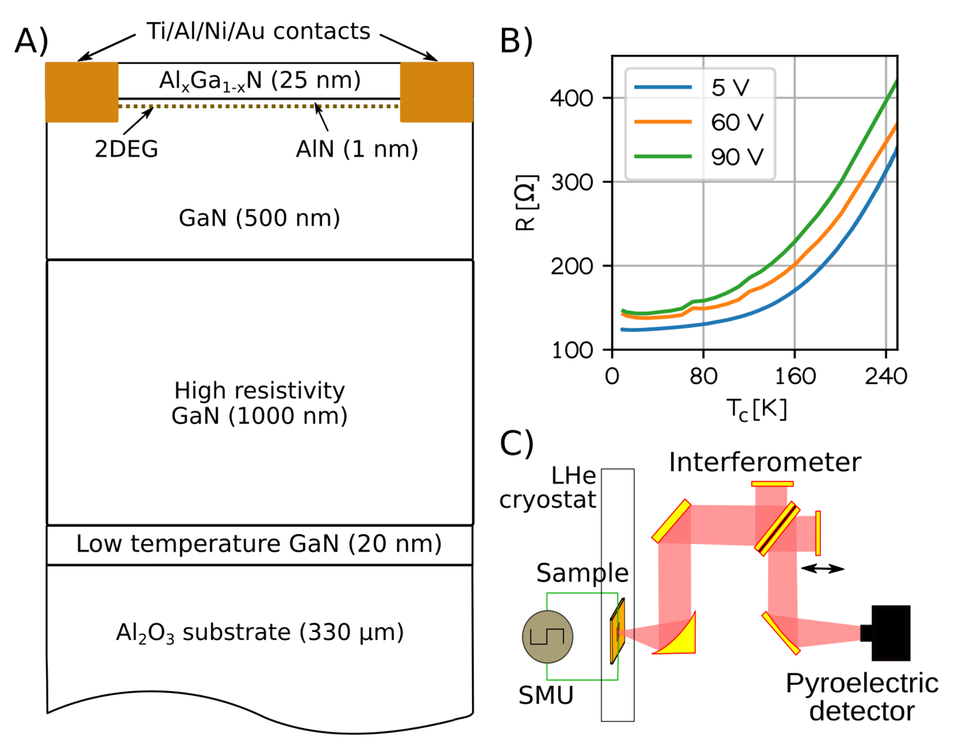
2. Materials and Methods
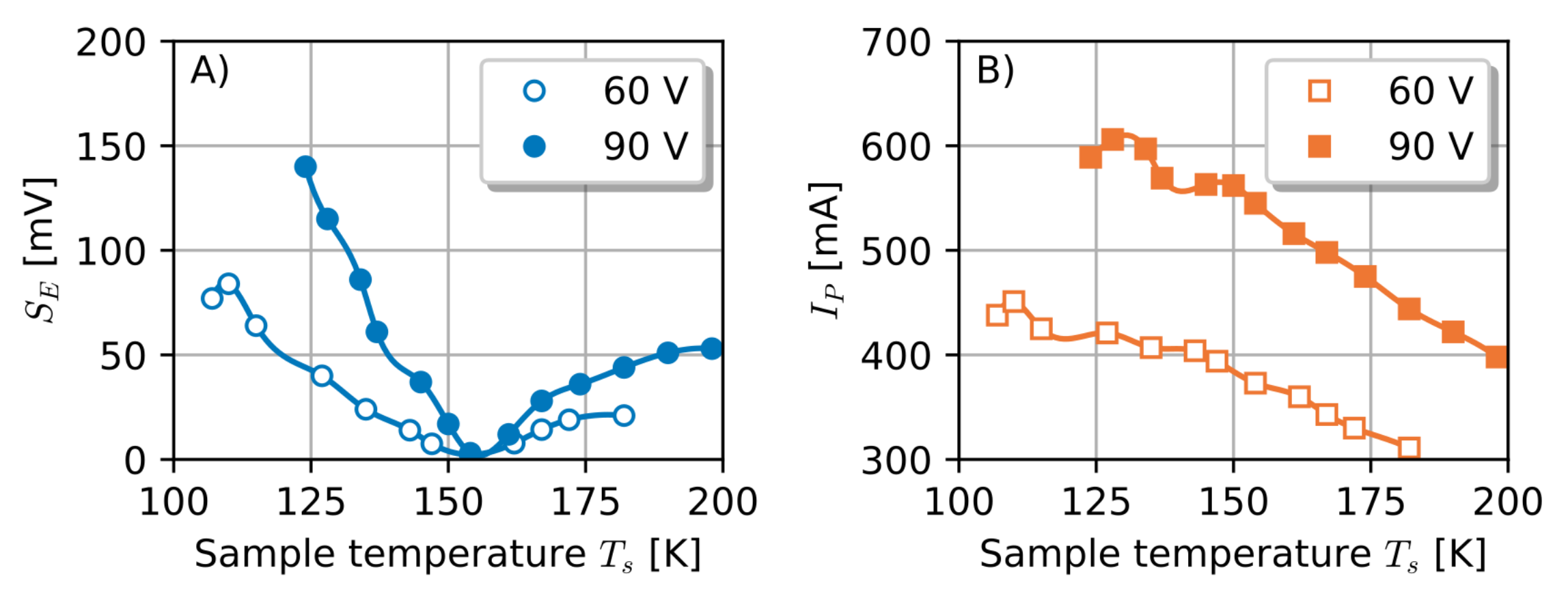
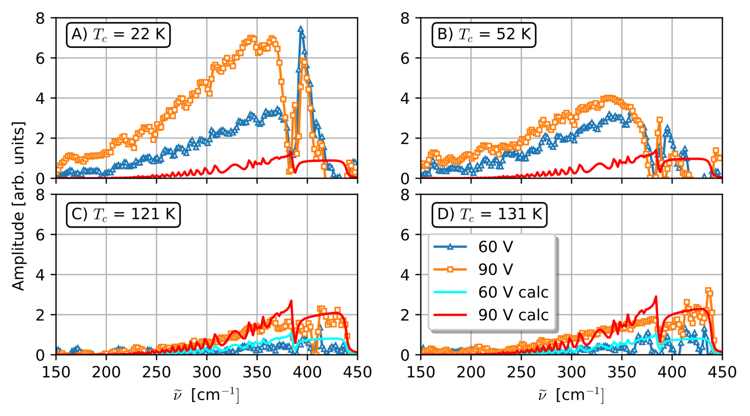
The investigated GaN/Al 0.2 Ga 0.8 N HEMT structures on Al 2 O 3 substrate (wafer No. TG2196) is depicted in Figure 1A. It was grown along c axis by the metal organic chemical vapor deposition [11]. The two-dimensional electron gas (2DEG) sheet concentration was n s = 9 × 10 12 cm 2 and Hall mobility measurements gave μ H = 1400 cm 2 / ( V · s ) and 4200 cm 2 / ( V · s ) at 293 and 77 K, respectively. Residual doping level was estimated to be below 10 17 cm 3 [12]. Two electrical ohmic contact stripes of 0.1 mm width and 2 mm length were formed at 2 mm distance from each other.
Large active area allowed to investigate the emission using a conventional far-infrared Fourier transform spectroscopy. The sample was kept in a closed-loop liquid helium cryostat with a TPX optical window. It was pumped electrically with voltage pulses of t p = 2.1 ms duration at modulation frequency of 7 Hz and bias amplitude up to U p = 90 V. The emitted radiation was collected with a short focal length off-axis parabolic mirror and directed to the input of Fourier spectrometer (“Thermo Scientific Nicolet-8700”) equipped with a SolidStateTM beam splitter and DTGS pyroelectric detector, operating in a step-scan mode. A lock-in technique was employed to demodulate the detected signal. Using this set-up, we were able to record emission spectra at the cryostat temperatures (measured at the cold finger) of 4–300 K in 50–600 cm 1 (1.5–18 THz) spectral range.

3. Results

The emission signal S E was detected at the cryostat cold finger temperature T c ranging from 10 K to 150 K at applied pulse voltages of 60 V and 90 V. Such voltages are heating up the sample, therefore its temperature T s differs from T c . To estimate T s at the bias, sample electrical resistance versus T c dependencies were measured (Figure 1B). The sample resistance dependence on temperature R ( T c ) was measured at U p = 5 V. As the sample heating during this measurement was found to be small, the assumption that T s = T c was made. Later, this curve was used as a reference in order to estimate the sample temperatures at different cryostat temperatures when U p = 60 V and 90 V. It was found indeed that at the bias of 60 V and 90 V the sample and cryostat cold finger temperatures differ significantly.
The emission intensity measured as a function of sample temperature T s is depicted in Figure 2A, whereas the current I P ( T s ) flowing through the sample is shown in Figure 2B. The emission signal is higher at low temperatures and decreases gradually until full signal suppression at T s = 155 K (at applied electrical power of 0.72 W and 0.33 W for U p = 60 V and 90 V, respectively). However, such a local minima is not observed in I P ( T s ) dependencies.
To gain a deeper understanding of the emission signal behavior described above, the spectra were measured at cryostat temperatures T c of 22 K, 52 K, 121 K, and 131 K, taking a few measuring points below and two above T s = 155 K. Figure 3 shows the emission spectra with the influence of the TPX window transmission and spectrometer’s beamsplitter efficiency removed. The spectra obtained below 155 K demonstrate the broad asymmetric peak with the weak spectral features in wavenumber range between 150 and 384 cm 1 . The upper range limit corresponds to the transverse optical sapphire phonon energy [13]. At higher wavenumbers, the sharp emission peak at the energy of longitudinal sapphire optical phonon energy ω LO = 387 cm 1 appears. Also, an intensive peak at 394 cm 1 is present, which could account for emission caused by radiative electron transitions in nitrogen vacancies in GaN [14].

4. Discussion

When T s > 155 K, the shape of emission spectra changes significantly (see Figure 3B,C for example). It has a rising character when wavenumbers increase; however, the dips are observed at the energies of Reststrahlen regions in sapphire. Therefore, it seems that the emission signal reaching the detector is the product of a black-body spectral radiance B ( ω , T ) and thermal emissivity E ( ω , T ) of the sample:
S ( ω , T ) = B ( ω , T ) · E ( ω , T ) .
According to Kirchhoff law, thermal emissivity is equal to sample absorptance E ( ω , T ) = α ( ω , T ) = 1 t ( ω , T ) r ( ω , T ) , where t ( ω , T ) and r ( ω , T ) are the transmittance and reflectance of the sample. To determine t ( ω , T ) and r ( ω , T ) the numerical implementation of Rigorious Coupled-Wave Analysis (RCWA) method was used [15]. The sample itself was considered to stay in vacuum environment and its dielectric function ε sl ( ω ) was modeled as a sum of dielectric functions of each layer. To estimate the dielectric function of a single layer, the phononic term was involved, and taken in factorized form [16]:
ε ph ( ω ) = ε i = 1 l ω TO , i 2 ω 2 j ω γ TO , i ω LO , i 2 ω 2 j ω γ LO , i .
Here, ε denotes high frequency dielectric permitivitty, ω TO ( LO ) and γ TO ( LO ) – TO(LO) phonon energy and damping factor, respectively. The multiplication operation is performed over the number l of those IR-active optical phonon modes which create the dipole moment normal to c -axis ( E l symmetry). The temperature dependent values of ω TO ( LO ) and γ TO ( LO ) for sapphire were taken from [16] and ε = 3.08 . In case of GaN, however, damping weakly depends on temperature in the interval from 85 K to 200 K [17], and γ TO = γ LO = 8 cm 1 was kept, whereas ε = 5.35 .
Two-dimensional electron thermal emission was not included in the calculations, as the intensity of such emission is at least a few orders of magnitude lower than the black-body radiation in a spectral range in which the experiment was conducted [18].
The black-body radiation of the sample was calculated using the parameters given above. The black-body spectral intensity is estimated as a difference of spectral intensity at a sample temperature at pumping pulse and the cryostat cold finger temperature: B ( ν ˜ , T ) = B ( ν ˜ , T p ) B ( ν ˜ , T b ) . An approximate value of T p was found from sample resistance dependence on temperature (see Figure 1B). T c = 121 K and 131 K corresponds to T s = 185 K and 193 K when U p = 90 V, and to T s = 162 K and 167 K when U p = 60 V. Theoretically calculated emission intensity is presented as solid curves in Figure 3. As it was assumed, its shape agrees well with the experimentally observed results, when the sample temperature is above 155 K. In addition, the dips in the Reststrahlen bands of sapphire are resolved in the spectra at 384–387 cm 1 (l = 1 sapphire optical phonon mode) and 440–482 cm 1 (l = 2). Also, the slope at 200–384 cm 1 coincides with experimental results, therefore a good agreement between experimental and calculated data shows that at T s > 155 K THz emission is caused by thermal radiation. Calculations were performed for the sapphire wafer only, and comparison showed, that the main contribution to emission spectra comes from sapphire substrate. Most probably, this result is the outcome of the fact that sapphire substrate thickness is much higher than the thickness of AlGaN/GaN heterostructure (330 μ m vs. 1.5 μ m, respectively).
At T s < 155 K, the emission signal cannot be described by Equation 1 as can be seen in panels A and B in Figure 3. The maximum of the broad intensity peak is located at ~350 cm 1 and does not move with voltage and temperature. Also, the intensity decreases with sample heating. Other physical mechanisms could be responsible for such behavior, for example electroluminescence from shallow Si, O, and C donors in unintentionally doped AlGaN and GaN layers [19].

5. Conclusions

The experimental investigation of electrically pumped THz emission from AlGaN/GaN HEMTs grown on sapphire substrate revealed that emission signal has a minima at T s = 155 K. The comparison of experimentally obtained THz spectroscopy data and theoretically calculated spectra showed that at temperatures above 155 K emission is caused by the thermal radiation of the sample. Also, at such temperatures, the emission spectra is mainly influenced by the thermal radiation coming from the sapphire substrate, which is much thicker than the AlGaN/GaN heterostructure. Other emission phenomena are dominating the net signal when the sample temperatures are below 155 K. Emission due to optical sapphire phonons is observed, also electroluminescence from shallow residual impurities could be responsible for the observed broadband THz emission. The results of our study also suggest that a better heat management should be provided in order to increase dissipation of electrical power and reduce thermal emission from the heated conductive channel, for example, the growth of AlGaN/GaN HEMT structures on native or SiC substrates.

Author Contributions

Conceptualization, I.K.; Methodology, I.K. and I.G.; Formal analysis, I.G.; investigation, I.G.; writing—original draft preparation, I.G.; writing—review and editing, I.K.; visualization, I.G.; supervision, I.K.; funding acquisition, I.G. All authors have read and agreed to the published version of the manuscript.

Funding

This research was funded by the European Social Fund under the No 09.3.3-LMTK-712 “Development of Competences of Scientists, other Researchers and Students through Practical Research Activities” measure.

Acknowledgments

The authors are grateful to Vytautas Jakštas for sample contacts processing and to Vytautas Janonis for the helpful advices concerning the RCWA calculations.

Conflicts of Interest

The authors declare no conflicts of interest. The funders had no role in the design of the study; in the collection, analyses, or interpretation of data; in the writing of the manuscript; or in the decision to publish the results.

Abbreviations

The following abbreviations are used in this manuscript:
THzterahertz
FETfield-effect transistor
HEMThigh-electron mobility transistor
2DEGtwo-dimensional electron gas
RCWArigorous coupled wave analysis

References

  1. Dhillon, S.; Vitiello, M.; Linfield, E.; Davies, A.; Hoffmann, M.C.; Booske, J.; Paoloni, C.; Gensch, M.; Weightman, P.; Williams, G.; et al. The 2017 terahertz science and technology roadmap. J. Phys. Appl. Phys. 2017, 50, 043001. [Google Scholar] [CrossRef]
  2. Łusakowski, J.; Teppe, F.; Dyakonova, N.; Meziani, Y.M.; Knap, W.; Parenty, T.; Bollaert, S.; Cappy, A.; Popov, V.; Shur, M.S. Terahertz generation by plasma waves in nanometer gate high electron mobility transistors. Phys. Status Solid. 2005, 202, 656. [Google Scholar] [CrossRef]
  3. Ikamas, K.; Nevinskas, I.; Krotkus, A.; Lisauskas, A. Silicon Field Effect Transistor as the Nonlinear Detector for Terahertz Autocorellators. Sensors 2018, 18, 3735. [Google Scholar] [CrossRef] [PubMed] [Green Version]
  4. Zagrajek, P.; Danilov, S.N.; Marczewski, J.; Zaborowski, M.; Kolacinski, C.; Obrebski, D.; Kopyt, P.; Salski, B.; But, D.; Knap, W.; Ganichev, S.D. Time Resolution and Dynamic Range of Field-Effect Transistor–Based Terahertz Detectors. J. Infrared Millim. Terahertz Waves 2019. [Google Scholar] [CrossRef] [Green Version]
  5. Otsuji, T.; Watanabe, T.; Moutaouakil, A.; Karasawa, H.; Komori, T.; Satou, A.; Suemitsu, T.; Suemitsu, M.; Sano, E.; Knap, W. Emission of terahertz radiation from two-dimensional electron systems in semiconductor nano-and hetero-structures. J. Infrared Millim. Terahertz Waves 2010, 32, 629. [Google Scholar] [CrossRef]
  6. El Fatimy, A.; Dyakonova, N.; Meziani, Y.; Otsuji, T.; Knap, W.; Vandenbrouk, S.; Madjour, K.; Théron, D.; Gaquiere, C.M.P. Nanofabrication Techniques and Their Applications to Terahertz Science and Technology. J. Appl. Phys. 2010, 107, 024504. [Google Scholar] [CrossRef] [Green Version]
  7. Lisauskas, A.; Rämer, A.; Burakevič, M.; Chevtchenko, S.; Krozer, V.; Heinrich, W.; Roskos, H.G. Terahertz emission from biased AlGaN/GaN high-electron-mobility transistors. J. Appl. Phys. 2019, 125, 151614. [Google Scholar] [CrossRef]
  8. Shalygin, V.A.; Moldavskaya, M.D.; Vinnichenko, M.Y.; Maremyanin, K.V.; Artemyev, A.A.; Panevin, V.Y.; Vorobjev, L.E.; Firsov, D.A.; Korotyeyev, V.V.; Sakharov, A.V.; et al. Selective terahertz emission due to electrically excited 2D plasmons in AlGaN/GaN heterostructure. J. Appl. Phys. 2019, 126, 183104. [Google Scholar] [CrossRef]
  9. Jakštas, V.; Grigelionis, I.; Janonis, V.; Valušis, G.; Kašalynas, I.; Seniutinas, G.; Juodkazis, S.; Prystawko, P.; Leszczyński, M. Electrically driven terahertz radiation of 2DEG plasmons in AlGaN/GaN structures at 110 K temperature. Appl. Phys. Lett. 2017, 110, 202101. [Google Scholar] [CrossRef]
  10. Grigelionis, I.; Jorudas, J.; Jakštas, V.; Janonis, V.; Kašalynas, I.; Prystawko, P.; Kruszewski, P.; Leszczyński, M. Terahertz electroluminescence of shallow impurities in AlGaN/GaN heterostructures at 20 K and 110 K temperature. Mater. Sci. Semicond. Process. 2019, 93, 280–283. [Google Scholar] [CrossRef]
  11. Jakštas, V.; Kašalynas, I.; Šimkienė, I.; Strazdienė, V.; Prystawko, P.; Leszczyński, M. Schottky diodes and high electron mobility transistors of 2DEG AlGaN/GaN structures on sapphire substrate. Lith. J. Phys. 2015, 54, 4. [Google Scholar] [CrossRef] [Green Version]
  12. Sai, P.; Jorudas, J.; Dub, M.; Sakowicz, M.; Jakštas, V.; But, D.B.; Prystawko, P.; Cywinski, G.; Kašalynas, I.; Knap, W.; Rumyantsev, S. Low frequency noise and trap density in GaN/AlGaN field effect transistors. Appl. Phys. Lett. 2019, 115, 183501. [Google Scholar] [CrossRef]
  13. Schubert, M.; Tiwald, T.E.; Herzinger, C.M. Infrared dielectric anisotropy and phonon modes of sapphire. Phys. Rev. B 2000, 61, 8187–8201. [Google Scholar] [CrossRef]
  14. Buckeridge, J.; Catlow, C.R.A.; Scanlon, D.O.; Keal, T.W.; Sherwood, P.; Miskufova, M.; Walsh, A.; Woodley, S.M.; Sokol, A.A. Determination of the Nitrogen Vacancy as a Shallow Compensating Center in GaN Doped with Divalent Metals. Phys. Rev. Lett. 2015, 114, 016405. [Google Scholar] [CrossRef] [PubMed] [Green Version]
  15. The RCWA MATLAB Code Was Developed for Free Release and Distribution in Professor Zhuomin Zhang’s Group at Georgia Institute of Technology. Available online: http://zhang-nano.gatech.edu/Rad_Pro.htm (accessed on 18 June 2018).
  16. Gervais, F.; Piriou, B. Anharmonicity in several-polar-mode crystals: adjusting phonon self-energy of LO and TO modes in Al2O3 and TiO2 to fit infrared reflectivity. J. Phys. Solid State Phys. 1974, 7, 2374. [Google Scholar] [CrossRef]
  17. Link, A.; Bitzer, K.; Limmer, W.; Sauer, R.; Kirchner, C.; Schwegler, V.; Kamp, M.; Ebling, D.G.; Benz, K.W. Temperature dependence of the E2 and A1(LO) phonons in GaN and AlN. J. Appl. Phys. 1999, 86, 6256–6260. [Google Scholar] [CrossRef]
  18. Shalygin, V.A.; Vorobjev, L.E.; Firsov, D.A.; Sofronov, A.N.; Melentyev, G.A.; Lundin, W.V.; Nikolaev, A.E.; Sakharov, A.V.; Tsatsulnikov, A.F. Blackbody-like emission of terahertz radiation from AlGaN/GaN heterostructure under electron heating in lateral electric field. J. Appl. Phys. 2011, 109, 073108. [Google Scholar] [CrossRef]
  19. Grigelionis, I.; Prystawko, P.; Jorudas, J.; Kašalynas, I. Electrically-controlled THz emission from AlGaN/GaN/Al2O3 high electron mobility transistor structures at a temperature of 20 K. In Proceedings of the 2019 44th International Conference on Infrared, Millimeter, and Terahertz Waves (IRMMW-THz), Paris, France, 6 September 2019; pp. 1–2. [Google Scholar] [CrossRef]
Figure 1. The layer composition of investigated AlGaN/GaN HEMT structure (A). Sample resistance dependencies on cryostat temperature at U p = 5 V, 60 V and 90 V (B). Schematics of spectroscopic experimental setup (C).
Applsci 10 00851 g001
Figure 2. (A) The temperature dependencies of pulsed emission signal S E . (B) Pulsed current I P in the sample at 60 V (full symbols) and 90 V (open symbols) pump voltages.
Applsci 10 00851 g002
Figure 3. Symbols denote Fourier transform terahertz emission spectra at cryostat itemperatures of 22 K, 52 K, 121 K, and 131 K (panels (AD), respectively) for pulse bias voltages of 60 V and 90 V. Solid curves denote the calculated thermal sample emission for cryostat base temperatures and bias voltages mentioned above.
Applsci 10 00851 g003

