Article

Rapid Optical Spin Initialization of a Quantum Dot in the Voigt Geometry Coupled to a Two-Dimensional Semiconductor

by
Dionisis Stefanatos
*,
Vasilios Karanikolas
,
Nikos Iliopoulos
and
Emmanuel Paspalakis
Materials Science Department, School of Natural Sciences, University of Patras, 26504 Patras, Greece
*
Author to whom correspondence should be addressed.
Appl. Sci. 2020, 10(3), 1001; https://doi.org/10.3390/app10031001
Submission received: 4 December 2019 / Revised: 14 January 2020 / Accepted: 28 January 2020 / Published: 3 February 2020
(This article belongs to the Section Optics and Lasers)

Abstract

:
We study the interaction of a quantum dot in the Voigt configuration with a laser pulse and particularly analyze the potential for rapid spin initialization by putting the quantum dot near a molybdenum disulfide (MoS 2 ) monolayer. The MoS 2 monolayer influences the spontaneous decay rates of the quantum dot, leading to anisotropically enhanced decay rates, for the quantum dot’s electric dipole moments parallel and perpendicular to the layer. By solving the relevant density matrix equations, we find that high spin initialization fidelity is obtained at short times. The fidelity is significantly higher than when the quantum dot is in free-space vacuum. We examine two different cases of the interaction of the quantum dot with the applied optical field. First, we use a continuous wave laser field and determine for various quantum dot—MoS 2 layer distances the field strength that leads to acceptable fidelity levels. The effect of the quality of the MoS 2 material on the fidelity of spin initialization is also examined. We also study the interaction of the quantum dot with a laser pulse and apply numerical optimal control to obtain the time-dependent field strength, which leads to maximum final fidelity for short time intervals. The latter approach gives beneficial results in comparison to the continuous wave field excitation.

1. Introduction

Quantum dots (QDs), also known as “artificial atoms”, are primary candidates for quantum information technologies [1]. An important structure is based on the electron spin states of a QD in the so-called Voigt geometry, which form the basic qubit, where one applies a magnetic field at a direction perpendicular to the growth axis of the QD [2,3,4,5,6,7,8,9,10,11,12,13,14,15,16,17,18,19,20,21,22]. The basic energy level scheme for a negatively charged QD in the Voigt configuration (see Figure 1a) consists of four energy levels. The lower levels | 1 and | 2 are for the electron spin states, and the two upper levels are for the trion states. Naturally, the QD is in an incoherent mixture state, with equal population distribution among the two spin states | 1 and | 2 . An important problem in this system is initialization, i.e., the creation of a particular electron spin state [10,14,15,16,17,19,20,21,22], which can be succeeded by the optical pumping method. Specifically, a linearly polarized optical field excites resonantly the QD system and couples one of the electron spin states to a specific trion state (let us assume it couples state | 1 to state | 4 ). Then, by spontaneous emission pumping of the population, the other spin state (in our example state | 2 ) is obtained after a few decay times. During the pumping process, the population also returns back to state | 1 due to spontaneous decay. This population needs to be pumped again, and this slows down the initialization process. Loo et al. proposed the idea to accelerate the optical initialization process by utilizing a preferential Purcell-accelerated deexcitation towards the desired target state [14] (in our example state | 2 ). The key to their proposal is to create an anisotropic Purcell-enhanced decay rate from the trion state to the target electron spin state by coupling the QD with a photonic structure. This idea has been explored by coupling the QD with various microphotonic and nanophotonic structures, like a semiconductor micropillar cavity, a photonic crystal nanocavity [15], a metallic prolate spheroidal nanoparticle [16], a metallic bow tie nanoantenna [17], and a planar metallo-dielectric nanostructure [19].
Recently, our group proposed the coupling of a QD in the Voigt geometry with a graphene monolayer, the basic two-dimensional material, for obtaining high fidelity electron spin initialization in short time intervals [22]. Here, we analyze a different two-dimensional material for accelerating the optical pumping process in a QD in the Voigt configuration. Specifically, the QD is placed next to a two-dimensional semiconductor, a molybdenum disulfide (MoS 2 ) monolayer, as shown in Figure 1b. MoS 2 is an atomically thin, two-dimensional, direct bandgap semiconductor [23,24,25]. It features a bandgap in the visible, strong excitonic resonances, and high oscillator strengths. MoS 2 also supports exciton-polaritons, and it has been predicted theoretically that it can modify the spontaneous decay rates for nearby quantum emitters [26,27,28,29]. Experiments with coupled quantum emitters (quantum dots and molecules) and MoS 2 layers have also appeared in the literature [30,31,32,33]. The spontaneous decay rates for a quantum emitter near a MoS 2 layer can be anisotropic for electric dipole moments parallel or perpendicular to the monolayer [28], which makes the MoS 2 layer a potential candidate for accelerating the spin initialization process in a nearby QD in the Voigt geometry. Here, we first compute the Purcell factors for the QD near a MoS 2 monolayer. Then, we solve the density matrix equations with the modified Purcell factors and investigate the fidelity of spin initialization under optical pumping conditions. We examine two different cases of interaction of the QD with the applied optical field. First, we use a continuous wave laser field and determine for various QD − MoS 2 layer distances the field strength that leads to acceptable fidelity levels. The effect of the quality of the MoS 2 material, as well as the effect of the host dielectric environment permittivity, on the fidelity of spin initialization, are examined. We also study the interaction of the QD with a laser pulse and apply numerical optimal control, using a state-of-the-art optimal control solver, to obtain the time-dependent field strength, which leads to maximum final fidelity for short time intervals. The latter approach gives beneficial results in comparison to the continuous wave field excitation. We also find that the resulting optimal pulse is robust to positioning error of the QD − MoS 2 monolayer structure and to additive constant control error.
The paper has the following structure. In the coming section, we present the density matrix equations for the interaction of the QD in the Voigt geometry with a resonant optical field near the MoS 2 monolayer. Section 3 contains the basic results of the paper for the creation of rapid spin initialization with high fidelity using the interaction of the QD with laser fields with constant and time-dependent field strengths. Finally, in Section 4, we summarize our findings.

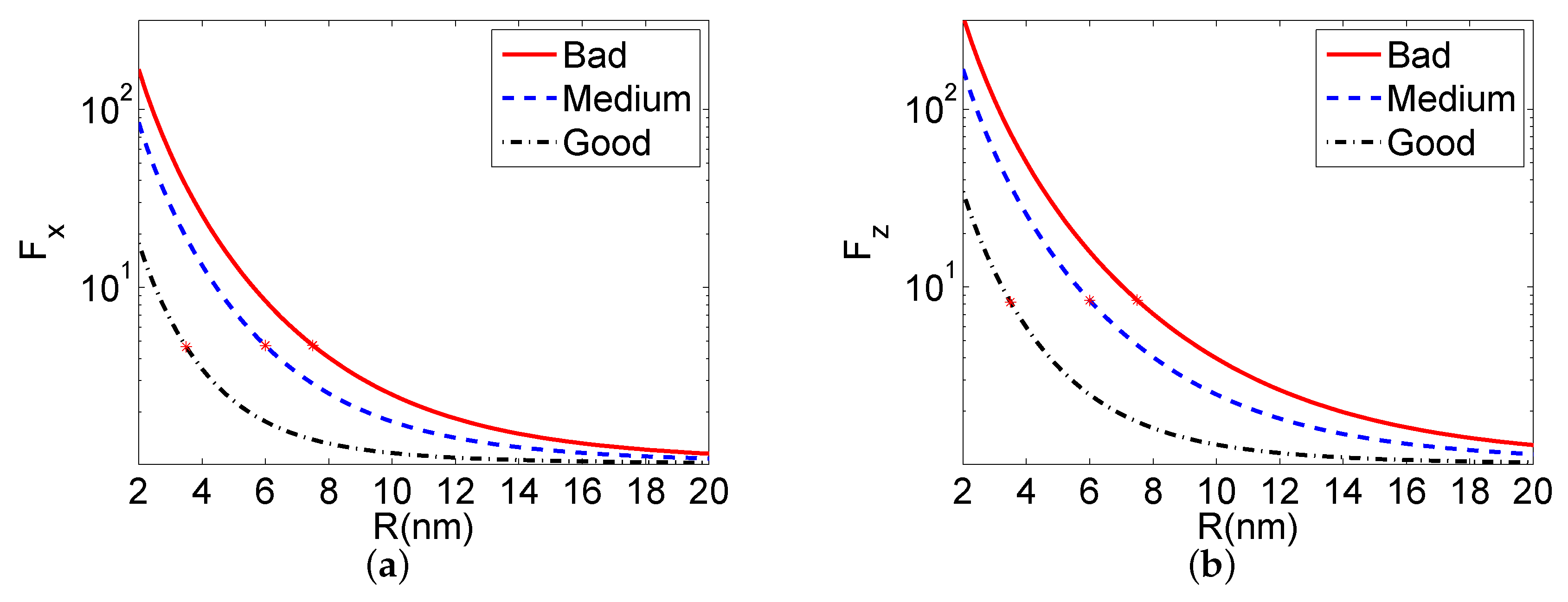
2. Density Matrix Equations for the QD Near a MoS 2 Monolayer under Interaction with an Optical Field

As we have already mentioned above, we study a singly-charged self-assembled QD. The growth axis of the QD was the y-axis, and an external magnetic field with the direction in the x-axis was applied to the QD. This created the QD in the Voigt geometry and lifted the degeneracy of the electron/hole levels by Zeeman splitting. Then, the ground spin energy levels were | 1 = | x and | 2 = | x , and the excited trion energy levels were | 3 = | x x x and | 4 = | x x x (see Figure 1a for the actual level structure). With ( ) and ( ) , we denote electron spins and heavy-holes, respectively. Here, the transitions | 1 | 4 and | 2 | 3 have x-polarized dipole moments, and the transitions | 1 | 3 and | 2 | 4 have z-polarized dipole moments. The goal of this paper is to create spin state | 2 . Therefore, we considered the interaction of the QD with a x-polarized optical field, which drives at exact resonance the transition | 1 | 4 , and then electron spin state | 2 is created by optical pumping.
The dynamics of the interaction of the QD with the optical field is studied by the density matrix equations. If we take the laser frequency of the applied field at exact resonance with the | 1 | 4 transition, the density matrix equations, under the dipole and rotating wave approximations, take the form:
(1) ρ ˙ 11 = γ 41 ρ 44 + γ 31 ρ 33 2 Ω ρ 41 I , (2) ρ ˙ 22 = γ 32 ρ 33 + γ 42 ρ 44 + 2 Ω ρ ˜ 23 I , (3) ρ ˙ 33 = ( γ 31 + γ 32 ) ρ 33 2 Ω ρ ˜ 23 I , (4) ρ ˙ 44 = ( γ 41 + γ 42 ) ρ 44 + 2 Ω ρ 41 I , (5) ρ ˙ 41 I = γ 41 + γ 42 2 ρ 41 I + Ω ( ρ 11 ρ 44 ) , (6) ρ ˜ ˙ 23 R = γ 31 + γ 32 2 ρ ˜ 23 R + ( ω 21 + ω 43 ) ρ ˜ 23 I , ρ ˜ ˙ 23 I = γ 31 + γ 32 2 ρ ˜ 23 I ( ω 21 + ω 43 ) ρ ˜ 23 R (7) + Ω ( ρ 33 ρ 22 ) ,
where ρ n m = ρ m n * , and we defined ρ ˜ 23 = ρ 23 e i ( ω 41 + ω 43 ) t . Furthermore, with the superscripts R , I , we denote, respectively, the real and imaginary part. The energy of level | n is ω n , n = 1 , 2 , 3 , 4 , , and the time-dependent, in general, Rabi frequency, which determines the interaction of the QD with the applied laser field, is Ω ( t ) . As we took the laser field to be at exact resonance with the transition | 1 | 4 , we chose its frequency as ω 0 = ω 4 ω 1 = ω 41 . We note that the dynamics that will be studied below will be from a few hundred ps to some ns. The spin-flip trion relaxation that may connect directly states | 4 and | 3 had a characteristic time of 1 μ s [10], so it did not contribute in the system dynamics in the time scales of interest, and it was omitted. This approximation was done in all relevant studies; see, e.g., [10,11,12,13,14,15,16,17,18,19,20,21,22].
The density matrix equations also include the effect of spontaneous decay from the trion to the spin states, where γ n m denotes the spontaneous decay rate for the transition | n | m with:
γ 41 = γ 32 = γ x = F x γ , γ 42 = γ 31 = γ z = F z γ ,
and γ is the free-space decay rate, for which we use the value γ = 1.2 μ eV [10,21] in the calculations. Furthermore, F l , with l = x , z , is the Purcell factor for the influence of the MoS 2 monolayer on the spontaneous decay rates.
The geometry we considered contains a homogeneous host dielectric environment with permittivity ε 1 with a MoS 2 monolayer in it; see Figure 1b. The MoS 2 monolayer lied on the x y plane at z = 0 . The QD was at distance z = R above the monolayer. The Purcell factors at z = R were calculated from first-order perturbation theory, with the application of Fermi’s golden rule, summing over all final states, and calculation of the relevant electromagnetic Green’s tensor at the position of the QD, with Green’s tensor representing the response of the geometry under consideration to a point-like excitation [34]. For details of the calculation, we refer the reader to [28]:
(9) F z = ε 1 + 3 c 2 ω Im i 0 d k s k s 3 k z 1 k 1 2 R N 11 e 2 i k z 1 R , (10) F x = ε 1 + 3 c 4 ω Im i 0 d k s k s k 1 R M 11 + k z 1 2 k 1 2 R N 11 e 2 i k z 1 R .
Here, k s , k z 1 = k 1 2 k s 2 denote the in-plane and perpendicular components of the wavevector, respectively, and k 1 = ω c ε 1 denotes the wavenumber in the host dielectric environment. Furthermore, R M 11 and R N 11 are the generalized Fresnel coefficients given by [35],
(11) R M 11 = α k 0 k z 1 + α k 0 , (12) R N 11 = α k 0 k z 1 k 1 2 + α k 0 k z 1
where α = 2 π σ / c and σ is the surface conductivity of MoS 2 .
The surface conductivity of the MoS 2 monolayer is given by:
σ ( ω ) = i ω χ 2 D ( ω ) ,
where the e h susceptibility, taking into account the two lower exciton energies, is given by the expression [29,36]:
χ 2 D ( ω ) = 4 e 2 v 2 π a e x 2 ω 2 g = A , B 1 E g ( ω + i γ g ) .
The two lower exciton energies are given by E A = 1.9 eV and E B = 2.1 eV . a e x = 0.8 nm was the exciton Bohr radius, and for MoS 2 we used the value v = 0.55 nm/fs [37]. We emphasize that the quality of the MoS 2 monolayer, which strongly depended on the material fabrication, was connected with the value of the damping parameters γ A and γ B ; the higher the value of the loss parameters, the worse the quality of the MoS 2 layer was. We defined the good quality MoS 2 for γ A = 0.5 meV and γ B = 1.1 meV, the medium quality MoS 2 for γ A = 2.5 meV and γ B = 5.6 meV, and the bad quality MoS 2 for γ A = 5.0 meV and γ B = 11.2 meV. We used the surface conductivity (13) in Equations (11) and (12).
Using the above relations, we could compute the Purcell factors for the QD near the MoS 2 monolayer. As the emission energy of the QD, we took ω 0 = 1.31 eV. In Figure 2, we display the distance dependence of the Purcell factors F x , F z by changing the distance between the QD and the MoS 2 monolayer. In the calculation, we assumed that ε 1 = 1 , i.e., that the host dielectric environment was free-space vacuum. We present results for three qualities of the semiconductor material in the layer, good (black dashed-dotted curve), medium (blue dashed curve), and bad (red solid curve). We observed that the worse the material quality was, the higher the Purcell factor became; at emission energies of ω 0 = 1.31 eV, the MoS 2 layer supported only lossy-surface-wave modes, which dissipated the QD’s energy. Hence, the highest value of the Purcell factor of the QD occurred for the bad quality MoS 2 .
In every case, an enhancement was obtained for the decay rates relevant to their vacuum values. Furthermore, a monotonic reduction of the decay rates with the increase of the distance R between the QD and the MoS 2 monolayer was found. In addition, for every distance, the decay rate corresponding to a dipole moment perpendicular to the monolayer (a dipole moment with z-orientation) was found to be always larger than the decay rate corresponding to a dipole moment parallel to the monolayer (a dipole moment with x-orientation). Therefore, the required anisotropically enhanced decay rates were obtained for a QD near a MoS 2 monolayer.

3. Rapid Spin Initialization with Optical Fields

The starting state of system of Equations (1)–(7) was ρ 11 ( 0 ) = ρ 22 ( 0 ) = 1 / 2 , ρ 33 ( 0 ) = ρ 33 ( 0 ) = ρ 41 I ( 0 ) = ρ ˜ 23 R ( 0 ) = ρ ˜ 23 I ( 0 ) = 0 . Below, we calculate the optical field, which maximized the fidelity of the target state | 2 when applied for given short durations. We examined both the cases of constant Rabi frequency Ω and time-dependent Rabi frequency Ω ( t ) .

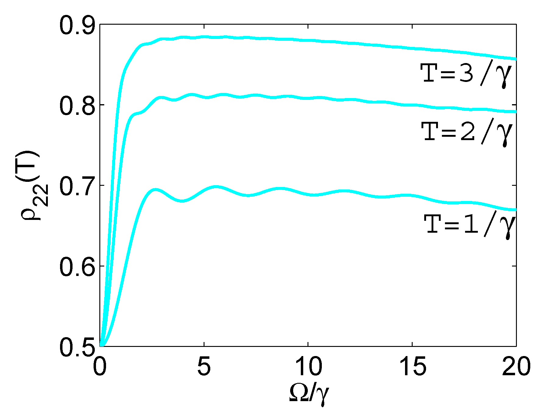
3.1. Constant Control

When the control Ω was constant, we could calculate analytically the final population (steady state) of the target state | 2 . From the equilibrium of Equations (1)–(7), we find:
ρ 22 ( ) = 1 + a 2 + b 2 4 + 2 a 2 + b 2 ,
where:
a = F x + F z 2 γ Ω , b = ω 21 + ω 43 Ω .
The time needed to arrive at the steady state could be estimated following [16], where the out-of-resonance transition | 2 | 3 was momentarily neglected. Under this assumption, state | 3 was decoupled, while states | 1 , | 2 , and | 4 formed a Λ system. Additionally, we could use equation ρ 11 = 1 ρ 22 ρ 44 to further eliminate ρ 11 , ending up with the reduced system:
(17a) ρ ˙ 22 = γ 42 ρ 44 , (17b) ρ ˙ 44 = ( γ 41 + γ 42 ) ρ 44 + 2 Ω ρ 41 I , (17c) ρ ˙ 41 I = γ 41 + γ 42 2 ρ 41 I + Ω ( 1 ρ 22 2 ρ 44 ) .
We could find an estimate of the necessary time to build ρ 22 by eliminating adiabatically ρ 44 , ρ 41 I , in which case, we obtained a rate equation for ρ 22 :
ρ ˙ 22 = r ( 1 ρ 22 ) ,
with:
r = F z 2 + a 2 γ
and a as in Equation (16).
We would like to reach high levels of ρ 22 as fast as possible. The goal could be obtained by choosing system parameters in a way to make both the population ρ 22 ( ) and the rate r large, but unfortunately, these objectives were conflicting. Observe that ρ 22 ( ) is a decreasing function of both Ω , F z , but r is an increasing function of Ω , while it depends non-monotonically on F z . The optimal parameters F x , F z , Ω were eventually determined from a compromise between these conflicting objectives.
Figure 3 displays contours of ρ 22 ( T ) as a function of the distance R between the QD −MoS 2 monolayer and the Rabi frequency Ω , for the three semiconductor qualities and three final times T = 1 / γ , 2 / γ , 3 / γ . Note that we used the Purcell factors F x , F z displayed in Figure 2. The three rows of the figure correspond to the three qualities (good, medium, and bad from top to bottom), while each column corresponds to a specific duration T. Observe from the second column of Figure 3, cases marked by red stars, that a high level ρ 22 ( T ) > 0.994 could be reached in a short time T = 2 / γ = 1.097 ns and for moderate Rabi frequency Ω = 5.17 γ . The corresponding optimal Purcell factors are listed in Table 1. In Figure 4, we display ρ 22 ( T ) in the absence of the monolayer, versus the Rabi frequency Ω and for the previously used durations. Note that in this case, ρ 22 ( T ) was less than 0.9 ; thus, the layer substantially sped up spin initialization. Figure 5 shows contour plots similar to those in Figure 3, but for three different permittivities of the dielectric host, ϵ 1 = 2 , 4 , 6 , when bad quality MoS 2 was used in the layer and the duration was set to T = 2 / γ = 1.097 ns. Observe that similar fidelity levels were obtained with the free-space vacuum case, although they slightly decreased with increasing permittivity. Finally, note that for larger permittivity values, the maximum fidelity was obtained for smaller distances between the QD and the monolayer.
Going back to Figure 3, note that for each quality (each row) and for larger durations (from left to right), the optimal value of ρ 22 ( T ) was attained for lower Ω and larger R, where the dependence on the distance corresponded actually to smaller F x + F z . This behavior could be understood since for larger times T, the steady state ρ 22 ( ) was approached, which is a decreasing function of Ω , F x + F z ; see Equations (15) and (16). Another interesting observation is that for each semiconductor quality and duration T, similar values of ρ 22 ( T ) were obtained, but at different distances from the monolayer. Thus, by choosing a different quality, we could change the optimal distance between the QD and the monolayer, which maximized electron spin initialization for the desired final time.

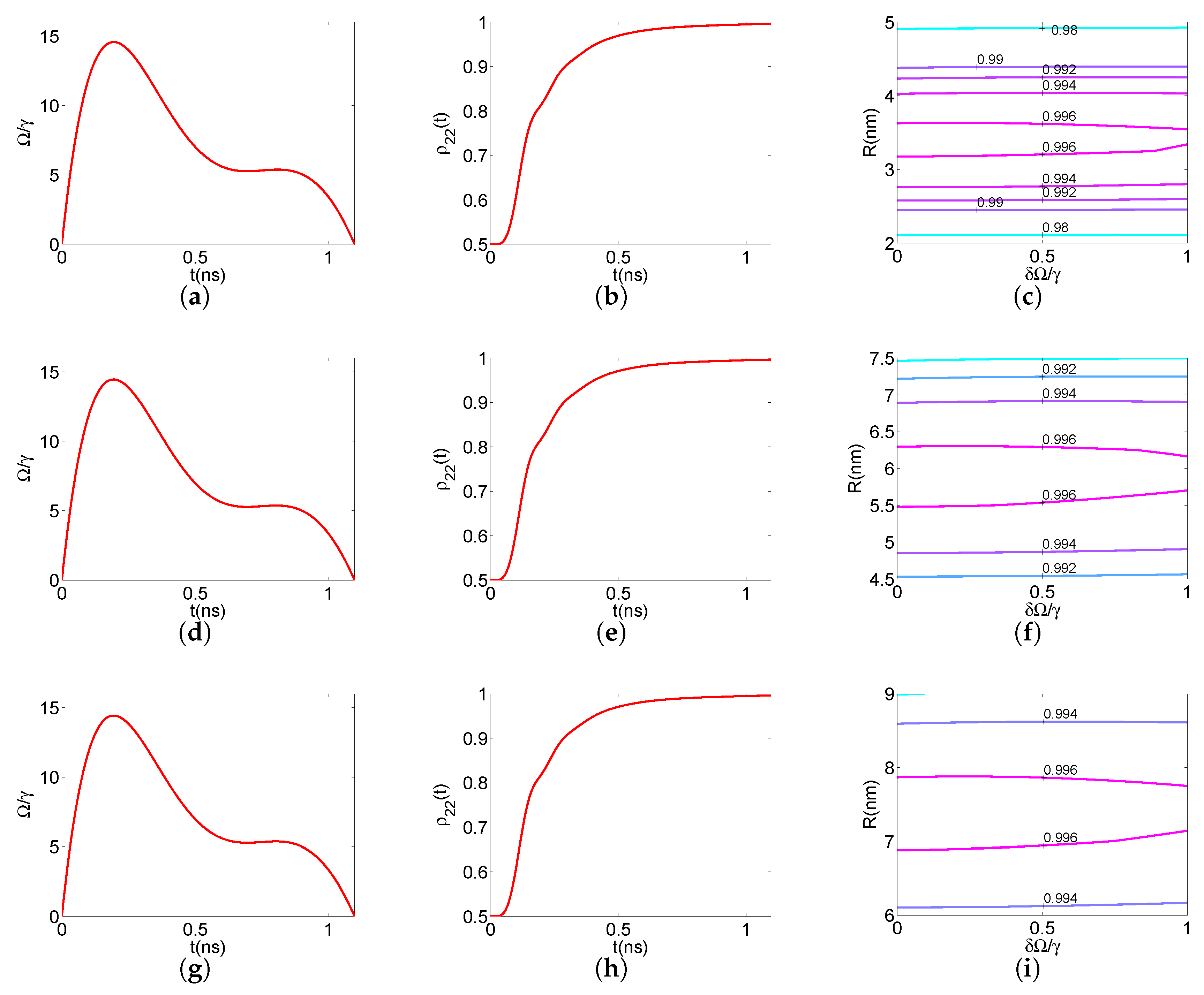
3.2. Time-Dependent Control

Here, we exploited numerical optimal control to find time-dependent Rabi frequency profiles Ω ( t ) that maximized ρ 22 ( T ) , while they vanished at t = 0 and t = T , i.e., they satisfied the boundary conditions:
Ω ( 0 ) = Ω ( T ) = 0 .
Such controls are easier to implement experimentally, since they do not contain jumps at the initial and final times.
The control Ω ( t ) was found using the BOCOP optimal control solver [38]. The advantages of this program are that it can take into account conditions as in Equation (20) and additionally offer the option to use as a control function a polynomial of time. Here, we treated the Rabi frequency Ω as an extra state variable, with boundary conditions (20), and used a polynomial control in the derivative:
d d τ Ω γ = k = 0 4 a k τ k ,
where τ = γ t is normalized time. Observe that we used a control polynomial of order four in the derivative, with coefficients a k to be found using the optimal control solver. The following condition was also imposed:
0 Ω ( t ) / γ 20 ,
to assure that the Rabi frequency lied within values that were feasible for experimental implementation. The optimal control problem for Equations (1)–(7), augmented by Equation (21) for Ω , was to determine the coefficients a k that maximized ρ 22 ( T ) for a given final time T, while the constraints (20) and (22) were satisfied. After calculating these optimal a k , we could find the corresponding Rabi frequency profile by integrating Equation (21):
Ω ( t ) γ = m = 1 5 a m 1 m ( γ t ) m .
The examples that we considered corresponded to the three cases marked with red stars in the second column of Figure 3: good quality semiconductor layer at R = 3.5 nm, medium quality semiconductor layer at R = 6 nm, and bad quality semiconductor layer at R = 7.5 nm. In all the examples, the duration was set to T = 2 / γ = 1.097 ns. The optimal coefficients found using BOCOP are listed in Table 2. In Figure 6, we display for each case (for each row, the order is good, medium, bad, from top to bottom) the resulting control field Ω ( t ) (first column) and the corresponding evolution ρ 22 ( t ) (second column). Observe that the shape of the optimal Ω ( t ) was similar for all the cases, as was also verified by examining the coefficients a k in Table 2, which were close to each other. The reason was that the Purcell factors used in the system of Equations (1)–(7) were similar for all three cases; see Table 1 or Figure 2 (points highlighted with a red star). The common final value ρ 22 ( T ) = 0.9963 exceeded the final value 0.9945 found using constant Rabi frequency Ω = 5.17 γ in the second column of Figure 3. In the last column of Figure 6, we plot contours of ρ 22 ( T ) for a positioning error | δ R | 1.5 nm around the nominal value R = 3.5 , 6 , 7.5 nm of each case and an additive constant error in the control 0 δ Ω / γ 1 . The final value ρ 22 ( T ) was quite robust with respect to the amplitude error, while values ρ 22 ( T ) 0.994 were found for a positioning error between 0.5 1 nm, depending on the case. Note that, with respect to positioning error, the case with a bad quality semiconductor layer at R = 7.5 nm (Figure 6i) was more robust than that of a medium quality layer at R = 6 nm (Figure 6f), which in turn was more robust than the case with a good quality layer at R = 3.5 nm (Figure 6). Such a behavior can be explained by inspecting the diagrams of Figure 2, which show the dependence of Purcell factors versus the distance R. The slope in these plots corresponds to the sensitivity of Purcell factors in changes of R, i.e., to positioning errors. It was obvious that for the cases of interest, highlighted with red stars, a smaller slope corresponded to the more robust situations. Similar results were also obtained for different host dielectric material permittivities (not shown here).

4. Conclusions

In this article, we continued our studies in accelerating spin initialization for a QD in the Voigt configuration using nearby two-dimensional materials [22] by studying the problem of a QD near a MoS 2 monolayer and studied in detail the fidelity for initialization under different excitation processes and different MoS 2 material qualities and host dielectric material permittivities. By calculating the modified spontaneous emission rates for a QD near the MoS 2 monolayer and using the results in the corresponding density matrix equations, we showed that highly efficient electron spin initialization was obtained for short time intervals. The fidelities obtained were much higher than for the QD in free-space. We examined two different cases of the interaction of the QD with the applied optical field. First, we used a continuous wave laser field and determined for various QD − MoS 2 layer distances the field strength, which led to acceptable fidelity levels. The effect of the quality of the MoS 2 material, as well as the effect of the host dielectric environment permittivity on the fidelity of spin initialization were also examined. We also studied the interaction of the QD with a laser pulse and applied numerical optimal control, using a state-of-the-art optimal control solver, to obtain the time-dependent field strength, which led to maximum final fidelity for short time intervals. The latter approach gave beneficial results in comparison to the continuous wave field excitation. We also found that the resulting optimal pulse was robust to the positioning error of the QD − MoS 2 monolayer structure and to additive constant control error. The overall conclusion of this work was that high-fidelity rapid initialization of a QD in the Voigt geometry may occur near a MoS 2 monolayer using both excitation methods, for different material qualities and different host dielectric material permittivities. The fidelity and robustness was similar to that obtained for a QD near a graphene monolayer [22], so the MoS 2 monolayer was a valid alternative to graphene for achieving rapid initialization of a QD in the Voigt geometry.

Author Contributions

Conceptualization, E.P. and D.S.; methodology, D.S. and V.K.; software, D.S. and V.K.; validation, N.I.; investigation, V.K.; writing, original draft preparation, D.S., V.K., and E.P.; writing, review and editing, E.P., D.S., and N.I.; visualization, N.I.; supervision, E.P.; funding acquisition, E.P. All authors have read and agreed to the published version of the manuscript.

Funding

The research is implemented through the Operational Program “Human Resources Development, Education and Lifelong Learning” and is co-financed by the European Union (European Social Fund) and Greek national funds (Project EΔBM34, Code MIS 5005825).

Conflicts of Interest

The authors declare no conflict of interest.

Abbreviations

The following abbreviations are used in this manuscript:
QDQuantum dot

References

  1. Michler, P. (Ed.) Quantum Dots for Quantum Information Technologies; Springer: Berlin/Heidelberg, Germany, 2017. [Google Scholar]
  2. Warburton, R.J. Single spins in self-assembled quantum dots. Nat. Mater. 2013, 12, 483–493. [Google Scholar] [CrossRef] [PubMed]
  3. Gao, W.B.; Imamoglu, A.; Bernien, H.; Hanson, R. Coherent manipulation, measurement and entanglement of individual solid-state spins using optical fields. Nat. Photonics 2015, 9, 363–373. [Google Scholar] [CrossRef]
  4. Xu, X.; Wu, Y.; Sun, B.; Huang, Q.; Cheng, J.; Steel, D.G.; Bracker, A.S.; Gammon, D.; Emary, C.; Sham, L.J. Fast spin state initialization in a singly charged InAs-GaAs quantum dot by optical cooling. Phys. Rev. Lett. 2007, 99, 097401. [Google Scholar] [CrossRef] [PubMed] [Green Version]
  5. Press, D.; Ladd, T.D.; Zhang, B.; Yamamoto, Y. Complete quantum control of a single quantum dot spin using ultrafast optical pulses. Nature 2008, 456, 218–221. [Google Scholar] [CrossRef] [PubMed]
  6. Delteil, A.; Sun, Z.; Gao, W.-B.; Togan, E.; Faelt, S.; Imamoglu, A. Generation of heralded entanglement between distant hole spins. Nat. Phys. 2016, 12, 218–223. [Google Scholar] [CrossRef] [Green Version]
  7. Lagoudakis, K.G.; McMahon, P.L.; Fischer, K.A.; Puri, S.; Müller, K.; Dalacu, D.; Poole, P.J.; Reimer, M.E.; Zwiller, V.; Yamamoto, Y.; et al. Initialization of a spin qubit in a site-controlled nanowire quantum dot. New J. Phys. 2016, 18, 053024. [Google Scholar] [CrossRef]
  8. Sun, S.; Kim, H.; Luo, Z.; Solomon, G.S.; Waks, E. A single-photon switch and transistor enabled by a solid-state quantum memory. Science 2018, 361, 57–60. [Google Scholar] [CrossRef] [Green Version]
  9. Economou, S.E.; Sham, L.J.; Wu, Y.; Steel, D.G. Proposal for optical U(1) rotations of electron spin trapped in a quantum dot. Phys. Rev. B 2006, 74, 205415. [Google Scholar] [CrossRef]
  10. Emary, C.; Xu, X.; Steel, D.G.; Saikin, S.; Sham, L.J. Fast initialization of the spin state of an electron in a quantum dot in the Voigt configuration. Phys. Rev. Lett. 2007, 98, 047401. [Google Scholar] [CrossRef] [Green Version]
  11. Economou, S.E.; Reinecke, T.L. Theory of fast optical spin rotation in a quantum dot based on geometric phases and trapped states. Phys. Rev. Lett. 2007, 99, 217401. [Google Scholar] [CrossRef] [Green Version]
  12. Emary, C.; Sham, L.J. Optically controlled single-qubit rotations in self-assembled InAs quantum dots. J. Phys. Condens. Matter 2007, 19, 056203. [Google Scholar] [CrossRef] [Green Version]
  13. Sun, H.; Feng, X.-L.; Wu, C.; Liu, J.-M.; Gong, S.-Q.; Oh, C.H. Optical rotation of heavy hole spins by non-Abelian geometrical means. Phys. Rev. B 2009, 80, 235404. [Google Scholar] [CrossRef] [Green Version]
  14. Loo, V.; Lanco, L.; Krebs, O.; Senellart, P.; Voisin, P. Single-shot initialization of electron spin in a quantum dot using a short optical pulse. Phys. Rev. B 2011, 83, 033301. [Google Scholar] [CrossRef] [Green Version]
  15. Majumdar, A.; Kaer, P.; Bajcsy, M.; Kim, E.D.; Lagoudakis, K.G.; Rundquist, A.; Vuckovic, J. Proposed coupling of an electron spin in a semiconductor quantum dot to a nanosize optical cavity. Phys. Rev. Lett. 2013, 111, 027402. [Google Scholar] [CrossRef]
  16. Antón, M.A.; Carreño, F.; Melle, S.; Calderón, O.G.; Cabrera-Granado, E.; Singh, M.R. Optical pumping of a single hole spin in a p-doped quantum dot coupled to a metallic nanoparticle. Phys. Rev. B 2013, 87, 195303. [Google Scholar] [CrossRef] [Green Version]
  17. Carreño, F.; Arrieta-Yáñez, F.; Antón, M.A. Spin initialization of a p-doped quantum dot coupled to a bowtie nanoantenna. Opt. Commun. 2015, 343, 97–106. [Google Scholar] [CrossRef] [Green Version]
  18. Kumar, P.; Nakajima, T. Coherent population trapping in negatively charged self-assembled quantum dots using a train of femtosecond pulses. Phys. Rev. A 2015, 91, 023832. [Google Scholar] [CrossRef] [Green Version]
  19. Peng, Y.; Yun, Z.-Y.; Liu, Y.; Wu, T.-S.; Zhang, W.; Ye, H. Fast initialization of hole spin in a quantum dot-metal surface hybrid system. Physica B 2015, 470–471, 1–5. [Google Scholar] [CrossRef]
  20. Kumar, P.; Nakajima, T. Fast and high-fidelity optical initialization of spin state of an electron in a semiconductor quantum dot using light-hole-trion states. Opt. Commun. 2016, 370, 103–109. [Google Scholar] [CrossRef]
  21. Paspalakis, E.; Economou, S.E.; Carreño, F. Adiabatically preparing quantum dot spin states in the Voigt geometry. J. Appl. Phys. 2019, 125, 024305. [Google Scholar] [CrossRef]
  22. Stefanatos, D.; Karanikolas, V.; Iliopoulos, N.; Paspalakis, E. Fast spin initialization of a quantum dot in the Voigt configuration coupled to a graphene layer. Physica E 2020, 117, 113810. [Google Scholar] [CrossRef]
  23. Mak, K.F.; Lee, C.; Hone, J.; Shan, J.; Heinz, T.F. Atomically thin MoS2: A new direct-gap semiconductor. Phys. Rev. Lett. 2010, 105, 136805. [Google Scholar] [CrossRef] [PubMed] [Green Version]
  24. Wang, Q.H.; Kalantar-Zadeh, K.; Kis, A.; Coleman, J.N.; Strano, M.S. Electronics and optoelectronics of two-dimensional transition metal dichalcogenides. Nat. Nanotechnol. 2012, 7, 699–712. [Google Scholar] [CrossRef] [PubMed]
  25. Mak, K.F.; Shan, J. Photonics and optoelectronics of 2D semiconductor transition metal dichalcogenides. Nat. Photonics 2016, 10, 216–226. [Google Scholar] [CrossRef]
  26. Gartstein, Y.N.; Li, X.; Zhang, C.-W. Exciton polaritons in transition-metal dichalcogenides and their direct excitation via energy transfer. Phys. Rev. B 2015, 92, 075445. [Google Scholar] [CrossRef] [Green Version]
  27. Basov, D.N.; Fogler, M.M.; de Abajo, F.J.G. Polaritons in van der Waals materials. Science 2016, 354, aag1992. [Google Scholar] [CrossRef] [Green Version]
  28. Karanikolas, V.D.; Marocico, C.A.; Eastham, P.R.; Bradley, A.L. Near-field relaxation of a quantum emitter to two-dimensional semiconductors: Surface dissipation and exciton polaritons. Phys. Rev. B 2016, 94, 195418. [Google Scholar] [CrossRef] [Green Version]
  29. Karanikolas, V.D.; Paspalakis, E. Localized exciton modes and high quantum efficiency of a quantum emitter close to a MoS2 nanodisk. Phys. Rev. B 2017, 96, 041404. [Google Scholar] [CrossRef]
  30. Prins, F.; Goodman, A.J.; Tisdale, W.A. Reduced dielectric screening and enhanced energy transfer in single-and few-layer MoS2. Nano Lett. 2014, 14, 6087–6091. [Google Scholar] [CrossRef] [Green Version]
  31. Raja, A.; Montoya-Castillo, A.; Zultak, J.; Zhang, X.-X.; Ye, Z.; Roquelet, C.; Chenet, D.A.; van der Zande, A.M.; Huang, P.; Jockusch, S.; et al. Energy transfer from quantum dots to graphene and MoS2: The role of absorption and screening in two-dimensional materials. Nano Lett. 2016, 16, 2328–2333. [Google Scholar] [CrossRef]
  32. Schädler, K.G.; Ciancico, C.; Pazzagli, S.; Lombardi, P.; Bachtold, A.; Toninelli, C.; Reserbat-Plantey, A.; Koppens, F.H.L. Electrical control of lifetime-limited quantum emitters using 2D materials. Nano Lett. 2019, 19, 3789–3795. [Google Scholar] [CrossRef] [PubMed] [Green Version]
  33. Liu, H.; Wang, T.; Wang, C.; Liu, D.; Luo, J.-B. Exciton radiative recombination dynamics and nonradiative energy transfer in two-dimensional transition-metal dichalcogenides. J. Chem. Phys. C 2019, 123, 10087–10093. [Google Scholar] [CrossRef]
  34. Novotny, L.; Hecht, B. Priciples of Nano-Optics, 2nd ed.; Cambridge Universuty Press: Cambridge, UK, 2012. [Google Scholar]
  35. Hanson, G.W. Dyadic Green’s functions and guided surface waves for a surface conductivity model of graphene. J. Appl. Phys. 2008, 103, 064302. [Google Scholar] [CrossRef] [Green Version]
  36. Haug, H.; Koch, S.W. Quantum Theory of the Optical and Electronic Properties of Semiconductors, 5th ed.; World Scientific Publishing: Singapore, 2009. [Google Scholar]
  37. Vasilevskiy, M.I.; Santiago-Pérez, D.G.; Trallero-Giner, C.; Peres, N.M.R.; Kavokin, A. Exciton polaritons in two-dimensional dichalcogenide layers placed in a planar microcavity: Tunable interaction between two Bose-Einstein condensates. Phys. Rev. B 2015, 92, 245435. [Google Scholar] [CrossRef] [Green Version]
  38. Bonnans, F.; Martinon, P.; Giorgi, D.; Grélard, V.; Maindrault, S.; Tissot, O. BOCOP: An Open Source Toolbox for Optimal Control; INRIA-Saclay: Ile de France, France, 2017. [Google Scholar]
Figure 1. (a) A structure of the energy levels for a QD in the Voigt configuration. (b) A schematic of the system under study, where the QD is placed at distance z = R on top of a MoS 2 monolayer.
Applsci 10 01001 g001
Figure 2. The distance dependence of the Purcell factors for (a) x- and (b) z-orientations of the transition dipole moment. R is the distance between the QD and the MoS 2 monolayer, for three qualities of the semiconductor material: good (black dashed-dotted line), medium (blue dashed line), and bad (red solid line). The red stars highlight the values for the three examples of Figure 6.
Applsci 10 01001 g002
Figure 3. Contours of ρ 22 ( T ) as functions of the distance R between the QD and the monolayer and the Rabi frequency Ω , for the three MoS 2 qualities (three rows from top to bottom corresponding to good, medium, and bad) and different durations, (a,d,g) T = 1 / γ = 0.548 ns, (b,e,h) T = 2 / γ = 1.097 ns, and (c,f,i) T = 3 / γ = 1.645 ns.
Applsci 10 01001 g003
Figure 4. Final value ρ 22 ( T ) in the absence of the monolayer as a function of the Rabi frequency Ω , for various durations.
Applsci 10 01001 g004
Figure 5. Contours of ρ 22 ( T ) for duration T = 2 / γ = 1.097 ns versus the distance R between the QD-monolayer and the Rabi frequency Ω , for the bad quality MoS 2 and three values of the host dielectric permittivity, (a) ϵ 1 = 2 , (b) ϵ 1 = 4 , and (c) ϵ 1 = 6 . Observe that similar levels of fidelity are obtained with the case where the host medium is taken to be the free-space vacuum ( ϵ 1 = 1 ), although they are slightly reduced with increasing permittivity. Specifically, the maximum fidelities for the three displayed cases with ϵ 1 = 2 , 4 , 6 are 0.9943 , 0.9941 , 0.9939 , respectively.
Applsci 10 01001 g005
Figure 6. Three examples with optimized time-dependent control for duration T = 2 / γ = 1.097 ns: good quality MoS 2 layer at R = 3.5 nm (first row), medium quality MoS 2 layer at R = 6 nm (second row), and bad quality MoS 2 layer at R = 7.5 nm (third row). (a,d,g) Optimal control Ω ( t ) . (b,e,h) Corresponding ρ 22 ( t ) . The final value ρ 22 ( T ) = 0.9963 exceeds the value 0.9945 achieved with constant Rabi frequency in the second column of Figure 3. (c,f,i) Sensitivity diagram of ρ 22 ( T ) achieved with the optimal profile Ω ( t ) , for a positioning error around the nominal value R = 3.5 , 6 , 7.5 nm and a constant error δ Ω in the control.
Applsci 10 01001 g006
Table 1. Optimal Purcell factors related to the three cases marked by red stars in the second column of Figure 3, where the final time is T = 2 / γ = 1.097 ns: good quality MoS 2 layer at R = 3.5 nm, medium quality MoS 2 layer at R = 6 nm, and bad quality MoS 2 layer at R = 7.5 nm.
Purcell factorsGoodMediumBad
F x 4.644354.724924.73458
F z 8.233018.404878.43176
Table 2. Optimal coefficients a k , k = 0 , 1 , , 4 for the polynomial control (23) and the three examples that we consider: good quality MoS 2 layer at R = 3.5 nm, medium quality MoS 2 layer at R = 6 nm, and bad quality MoS 2 layer at R = 7.5 nm. In all the cases, the duration is set to T = 2 / γ = 1.097 ns.
CoefficientsGoodMediumBad
a 0 102.1785101.6637101.5777
a 1 −476.4625−475.7275−475.5947
a 2 642.1003644.4623644.8125
a 3 −333.5799−337.1246−337.6715
a 4 57.909359.071959.2532

