Article

Model Predictive Control Method Based on Deterministic Reference Voltage for Single-Phase Three-Level NPC Converters

School of Electrical and Electronics Engineering, Chung-ang University, Seoul 06974, Korea
*
Author to whom correspondence should be addressed.
Appl. Sci. 2020, 10(24), 8840; https://doi.org/10.3390/app10248840
Submission received: 11 November 2020 / Revised: 7 December 2020 / Accepted: 9 December 2020 / Published: 10 December 2020
(This article belongs to the Special Issue Design and Analysis of Electrical Machines and Drives)

Abstract

:
When single-phase three-level neutral-point-clamped (NPC) converters operate, there are two main control objectives that need to be met for correct operation. First, the ac source current must be controlled to be sinusoidal. Second, the dc capacitor voltages must be balanced. In original model predictive control (MPC) methods for NPC converters, an optimization process involving an empirical weighting factor design is required to meet both of these objectives simultaneously. This study proposes an MPC approach developed for single-phase three-level NPC converters to meet these objectives using a single reference voltage consisting of a difference-mode term and a common-mode term in each phase. The difference-mode term and the common-mode term are responsible for sinusoidal ac source current synthesis and dc capacitor voltage balancing, respectively. Then, a single cost function compares the adjusted reference voltage with possible voltage candidates to select an optimal switching state, resulting in the smallest cost function value. Different from the conventional MPC method, the proposed approach avoids the selection of weighting factors and the attendance of various control objectives. Thanks to the deterministic approach, the proposed MPC method is straightforward to implement and maintain fast transient performance while guaranteeing the control objectives. Finally, the effectiveness and feasibility of the proposed approach for single-phase three-level NPC are verified through comprehensive experimental results.

1. Introduction

Recently, single-phase three-level neutral point clamped (NPC) converters have been addressed for various applications, especially in the interface of renewable energy sources and storage system because of its reduced total harmonic distortion (THD), lower device power losses, and lower electromagnetic interference (EMI) compared with two-level converters [1,2,3,4,5,6,7,8]. Three-level NPC converters operated with model predictive control (MPC) methods, aided by fast and inexpensive microprocessors, are currently used to generate sinusoidal voltage and current [9,10,11,12]. Furthermore, NPC converters must maintain the balance of two dc capacitor voltages to avoid deteriorating output performance [13,14,15,16,17,18,19,20,21]. Hence, the two main control objectives that three-level NPC converters need to be met for correct operation are regulated sinusoidal source current and capacitor voltages’ balancing. MPC methods with multiple control objectives, as in the case of three-level NPC converters, commonly employ a cost function using weighting factors that consider proper pertinence and emphasis among control terms. The conventional MPC method determines a weighting factor that is mostly based on empirical procedures, although some research has been comprehensively explored to improve weighting factor selection work [22,23,24,25,26,27]. Therefore, it should be noted that the weighting factor tuning works are not straightforward and practical for implementation. Several studies have been conducted to eliminate the weighting factors of the model predictive control methods [28,29,30]. In [28], the capacitor voltage control part of the MPC method for the T-type converters was eliminated from the cost function. Thus, the corresponding weighting factor can be removed because the cost function only consists of the current control terms. In this algorithm, the capacitor voltage adjustment is obtained by selecting an appropriate small vector and a corresponding switching state to reduce the neutral point (NP) voltage unbalance in advance. Although this method can successfully eliminate the weighting factor, the capacitor voltage balance can be limited in operating regions with high reference voltage magnitude, which does not employ the small vectors. In [29], the MPC method with a three-step control procedure was developed to eliminate weighting factors for the T-type converters. The first step selects N switching states with the smallest errors using a cost function that controls only the capacitor voltage. In the second step, the cost function that controls only real and reactive power terms is used to select K number of switching states that minimize power errors among the N number of switching states. In the last step, the cost function that controls the switching frequency is used to select one of the K switching states to minimize errors. Although the proposed method based on the three cascading processes can implement the model predictive control method without the weighting factor, computational burden and calculation times of this control method can be increased due to the additional repetition steps. In [30], a Lyapunov-based finite control-set MPC was presented to achieve weighting factors’ elimination for the nested neutral- point-clamped converters but the complexity of this control scheme is high.
Based on the deterministic approach and previous work [31,32,33], this paper presents an MPC control scheme using a novel cost function design using only one reference voltage to achieve the multiple control objectives for single-phase three-level NPC converters. The reference voltage is generated by using a difference-mode voltage term and a common-mode term to regulate the source current and capacitor voltages’ balancing, respectively. The difference-mode voltage term for sinusoidal ac current generation forces the ac source current to follow the reference current, which is introduced as a bipolar voltage with a 180° phase difference between its a and b phases, as shown in Figure 1. In addition, the common-mode voltage term for the NP voltage balance is added to both the a and b phases and is calculated from the difference between the periodic samples of the two capacitor voltages. The common-mode voltage term, as proposed in this paper, which modifies the difference-mode reference voltage term to reduce the NP voltage imbalance, provides an inherent capability to obtain the NP voltage balance without weighting factor design. The optimal switching state, which achieves stated control objectives before, is selected by comparing the reference voltage with possible voltage candidates. The proposed MPC method avoids the selection of weighting factors and the attendance of various control objectives, compared with the conventional MPC method. The proposed method is straightforward to implement and maintains fast, transient performance while guaranteeing the control objectives. The precision and practicality of the proposed approach are confirmed by the presented experimental results using a prototype test.

2. Single-Phase NPC Converter Structure and Conventional MPC Approach

A single-phase three-level NPC converter, operating in rectifier mode, is shown in Figure 1. In the ac input side of the converter, a voltage source v s provides the source current i s through an ac side filter including input inductor L s and resistor R s . The output dc side is composed of two capacitors C and an output resistor load RL, where v c 1 and v c 2 indicate the dc capacitor voltages, and V d c represents the output dc side voltage. The input ac side is connected to the output dc side through two legs with eight switching devices and antiparallel diodes. The Insulated Gate Bipolar Transistors (IGBTs) and corresponding switching states in phase a and b are represented by S a j and S b j (j = 1, 2, 3, 4), respectively. The switching states of each phase can be described as
S x = {   1   i f   S x 1 , S x 2 :   O N 0   i f   S x 2 , S x 3 :   O N   1   i f   S x 3 , S x 4 :   O N   x = a ,   b ) .
In this, the upper and lower switches operate complementarily. The combination of switching states in Equation (1) generates nine different operating states in single-phase NPC operation. The possible switching state, the resulting switching status, the converter input voltage v a b , and corresponding capacitor voltages are shown in Table 1 for these nine states.
The nine operating states can generate the five-level input voltage v a b , which results in redundant operating states. As presented in Table 1, the two redundant states, (1, 0) and (0, −1), for ( S a , S b ) produce the same converter input voltage level but a different effect on the capacitor voltages. Likewise, the redundant states (0, 1) and (−1, 0) synthesize the same converter input voltage and opposite capacitor voltage behaviors. Hence, these redundant states will be used to control the capacitor voltages, v c 1 and v c 2 . The currents i c 1 and i c 2 , in Figure 1, are described by the operating status and the source current i s in Equations (2) and (3), respectively. Therefore, these currents are acquired without other measurements [28].
i c 1 = S a ( S a + 1 ) S b ( S b + 1 ) 2 i s
i c 2 = S a ( S a 1 ) S b ( S b 1 ) 2 i s
The dynamics of capacitor voltage in dc link are expressed as follows:
d v c x d t = 1 C i c x   ( x = 1 ,   2 )
Using a constant sampling period Ts, the capacitor voltage dynamics in the discrete-time domain is describe as
d v c x d t v c x ( k + 1 ) v c x ( k ) T s   ( x = 1 ,   2 )
where v c x ( k ) and v c x ( k + 1 ) represent the capacitor voltages at kth and (k + 1)th instant, respectively. Using Equation (5), the Equation (4) is described in the discrete-time domain as:
v c x ( k + 1 ) = v c x ( k ) + T s C i c x ( k )   ( x = 1 ,   2 )
Additionally, capacitor voltage variations during one sampling period, Δ v c x ( k ) = v c x ( k + 1 ) v c x ( k ) , from Equations (2), (3) and (6), is determined by the switching states, Sa and Sb, and the source current. The variance among the upper capacitor voltage and the lower capacitor voltage at the kth instant is described as:
v c ( g a p ) ( k ) = v c 1 ( k ) v c 2 ( k ) .
Furthermore, the difference between the two capacitor voltages in each sampling instant, Δ v c ( g a p ) ( k ) , can be deduced using Equations (2), (3) and (6) as:
Δ v c ( g a p ) ( k ) = Δ v c 1 ( k ) Δ v c 2 ( k )   = T s C ( S a 2 S b 2 ) i s ( k ) .
The ac source current of the converter is obtained as follows:
v s = R s i s + L s d i s d t + v a b .
The source current dynamic is deduced in the discrete-time domain as follows:
i s ( k + 1 ) = ( 1 R s T s L s ) i s ( k )   + T s L s ( v s ( k ) v a b ( k ) ) .
The predicted source current in Equation (10) can be changed following five possible values of the converter input voltage. Therefore, from Equations (7) and (8), the capacitor voltage balancing task can be carried out by adjusting the switching states S a ( k ) and S b ( k ) , whereas the source current is regulated by varying the input voltage, v a b ( k ) , as in Equation (10). Hence, the cost function, including the source current control term and the capacitor voltage balancing term, is obtained as
g = | i s * ( k + 1 ) i s ( k + 1 ) | + λ c | v c 1 ( k + 1 ) v c 2 ( k + 1 ) |
where λ c is a weighting factor to assign relative emphasis on the capacitor voltage balancing percentage. Besides, the predicted ac source reference current can be deduced from using the Lagrange extrapolation as
i s * ( k + 1 ) = 3 i s * ( k ) 3 i s * ( k 1 ) + i s * ( k 2 )
where i s * ( k ) is the current at the sampling instant k and i s * ( k 1 ) and i s * ( k 2 ) are the past current values at the sampling instants k 1 and k 2 , respectively. In addition, a delay compensation technique to alleviate the adverse effects of inevitable calculation delay needs a one-step further prediction of the ac source current and the future ac source reference current [34,35]. If Equations (6), (10) and (12) are shifted by one step forward, the future capacitor voltages, ac source current, and reference current at the (k + 2)th instant are obtained as:
v c x ( k + 2 ) = v c x ( k + 1 ) + T s C i c x ( k + 1 ) ( x = 1 ,   2 ) ,
i s ( k + 2 ) = ( 1 R s T s L s ) i s ( k + 1 ) + T s L s ( v s ( k + 1 ) ( k + 1 ) ) ,
and
i s * ( k + 2 ) = 3 i s * ( k + 1 ) 3 i s * ( k ) + i s * ( k 1 ) .
Likewise, by shifting Equation (11) by one step forward, the cost function for the delay compensation technique at the (k + 2)th instant is obtained as:
g = | i s * ( k + 2 ) i s ( k + 2 ) | + λ c | v c 1 ( k + 2 ) v c 2 ( k + 2 ) | .

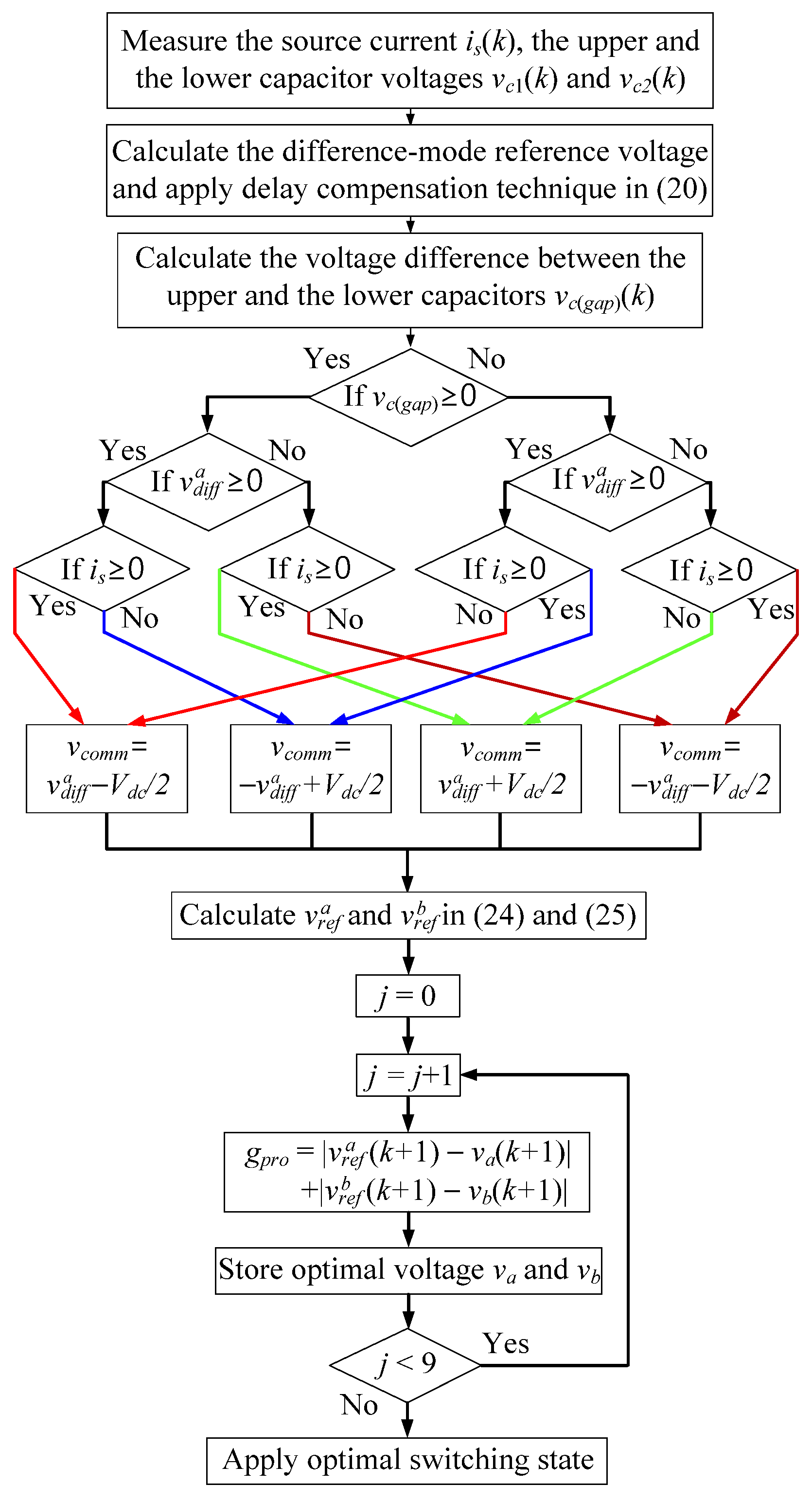
3. Proposed MPC Method

Since the purpose of the proposed method is to control two objectives using MPC with a single reference voltage and a cost function based on voltage instead of the current-based cost function in Equation (11), the reference voltage for source current regulation and capacitor voltages’ balancing should be derived. This paper developed the reference voltage as the sum of two voltage terms: the difference-mode reference voltage and the common-mode reference voltage. These reference voltages are for ac source current control and dc capacitor voltages’ balancing, respectively.

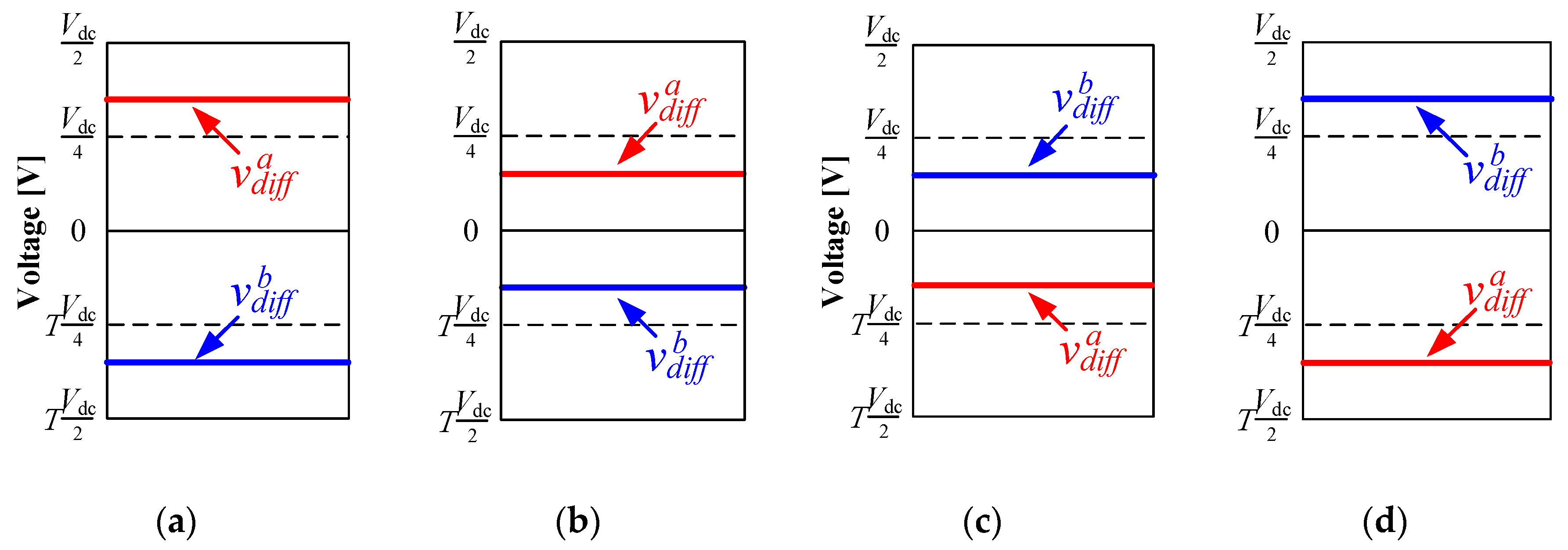
3.1. Difference-Mode Voltage Term for AC Source Current Generation

Replacing the one-step predicted source currents in Equation (10) with the one-step predicted current references, i s * ( k + 1 ) , and using the converter voltage reference v a b * ( k ) , the Equation (10) can be given as in [34,35]:
v a b * ( k ) = v s ( k ) R s i s ( k ) L s ( i s * ( k + 1 ) i s ( k ) ) T s
The a- and b-phase reference voltages, v d i f f a and v d i f f b , should be satisfied with the following relationship [13,36,37,38,39]:
v a b * ( k ) = v d i f f a ( k ) v d i f f b ( k ) = 2 v d i f f a ( k ) .
Thus, the a-phase reference voltage can be deduced from Equations (17) and (18) as:
v d i f f a ( k ) = 0.5 [ v s ( k ) R s i s ( k )   L s ( i s * ( k + 1 ) i s ( k ) ) T s ] .
By shifting Equation (19) one step forward for delay compensation [34,35], the a-phase reference voltage at k + 1 sampling instant, which can force the source current to follow the reference current, can be written as:
v d i f f a ( k + 1 ) = 0.5 [ v s ( k + 1 ) R s i s ( k + 1 )   L s ( i s * ( k + 2 ) i s ( k + 1 ) ) T s ] .
The resulting cost function can be described in Equation (21) with the reference voltage and actual voltage in each phase.
g p r o = | v d i f f a ( k + 1 ) v a ( k + 1 ) | + | v d i f f b ( k + 1 ) v b ( k + 1 ) |
where v a ( k + 1 ) and v b ( k + 1 ) denote the a-phase and b-phase voltages of the converter at the (k + 1)th step with respect to the neutral point “o”. The voltage-based cost function in Equation (21) compares reference voltages with the possible voltage candidates. Although there are two control objectives in Equation (21), the two terms are for the a-phase and b-phase voltage control in the converter, which always has the same weighting. As a result, the two terms do not use the weighting factor. The phase voltages of the converter, v a ( k + 1 ) and v b ( k + 1 ) , can take the values in Equation (22):
v x ( k + 1 ) = { V d c 2   ( S x 1 , S x 2 = 1 )   0   ( S x 2 , S x 3 = 1 ) V d c 2   ( S x 3 , S x 4 = 1 )   ( x = a ,   b )
It can be seen that the optimal switching state in the voltage-based cost function of Equation (21) is determined from the reference voltage because the MPC method selects a switching state resulting in the minimum cost function. For instance, if the a-phase reference voltage, v d i f f a , is higher than V d c / 4 and lower than V d c / 2 , as in Figure 2, the a-phase switching state Sa becomes one as seen from Equations (22) and (23). Because the two reference voltages v d i f f a and v d i f f b have the same magnitude with opposite polarities, there are four possible cases depending on the reference voltage positions, as shown in Figure 2.
Thus, an optimal switching state in each phase, calculated by the cost function in Equation (21), can be determined as a function of the difference-mode reference voltage by:
S i = { 1   ( V d c 4 v d i f f i V d c 2 ) 0   ( V d c 4 < v d i f f i < V d c 4 ) 1   ( V d c 2 v d i f f i V d c 4 ) ( i = a ,   b ) .
It can be seen from Equation (23) that the reference voltage positions in Figure 2a–d result in (1, −1), (0, 0), (0, 0), and (−1, 1) as the optimal operating states, respectively. The switching states determined by the difference-mode reference voltage can lead only to the three operating states, (1, −1), (0, 0), and (−1, 1), none of which can contribute NP voltage balancing because they force both the capacitor voltages to rise or fall together as shown in Table 1. As a result, in cases that capacitor voltages deviate from the nominal value, resulting in NP voltage unbalance, the MPC approach cannot minimize the differences between two capacitor voltages. Furthermore, it can be noted that only three-level line-to-line voltages with ± V d c and zero can be produced by the difference-mode reference voltages term. In this paper, a common-mode voltage term will be considered to add to the reference voltage in order to carry the capacitor voltages’ balancing task. In the next section, a common-mode voltage to regulate the NP voltage balance is added to the difference-mode voltage, which is for sinusoidal source current generation.

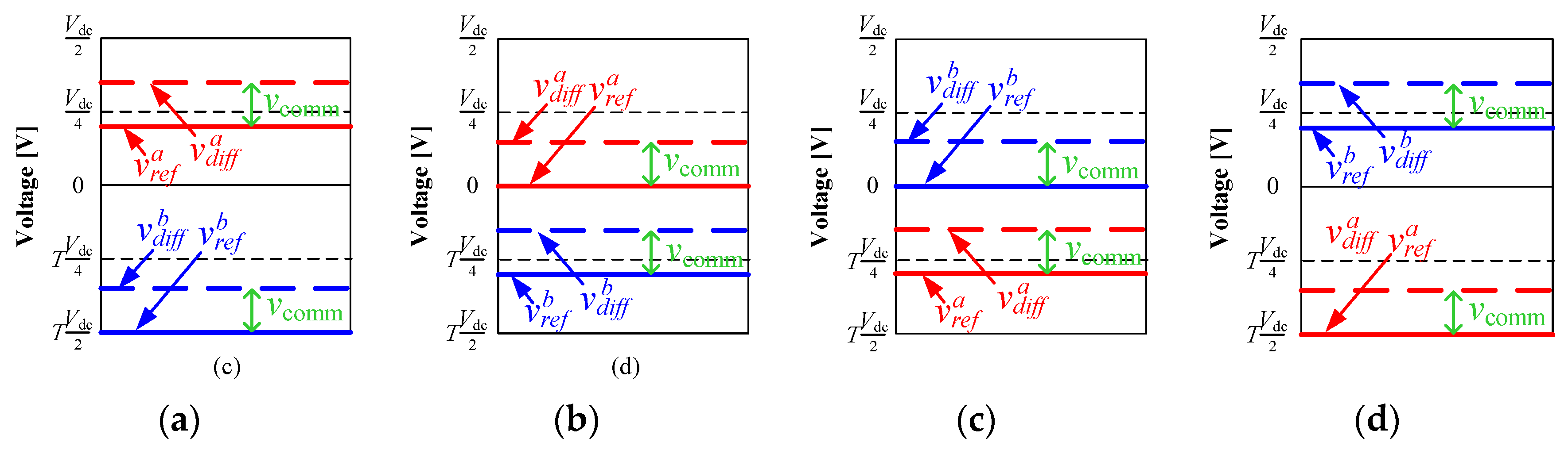
3.2. Common-Mode Voltage Term for Capacitor Voltage Balancing

For NP voltage balancing, the four switching states with redundancy in Table 1 need to be selected. As a result, the proposed method includes a common-mode reference voltage, which allows the reference voltage to select redundant switching states for NP voltage balancing. In the proposed MPC method, the reference voltage is defined by adding the difference-mode voltage term and the common-mode term as in:
v r e f a ( k + 1 ) =   v d i f f a ( k + 1 ) + v c o m m ( k + 1 )
v r e f b ( k + 1 ) =   v d i f f b ( k + 1 ) + v c o m m ( k + 1 ) .
The difference-mode voltage terms in the reference voltages deal with sinusoidal source current generation, whereas the common-mode voltage term employs the NP voltage balancing. Figure 3 shows that the reference voltages added by the positive common-mode voltage can change the positions of the difference-mode reference voltages shown in Figure 2. For example, Figure 3a illustrates that the difference-mode reference voltages, v d i f f a ( k + 1 ) and v d i f f b ( k + 1 ) , were placed just like Figure 2a. By adding the positive common-mode voltage, the reference voltages will be increased, as presented in Figure 3a. Changing the position of the reference voltages can make the operating state become (1, 0), as known from Equation (23), which corresponds to the redundant switching state for NP voltage balance control. Note that the switching state in Figure 3a can remain in (1, −1) after adding the common-mode voltage term v c o m m ( k + 1 ) if the magnitude of the positive common-mode voltage is small. Likewise, Figure 3c,d shows that the reference voltages with a positive common-mode voltage can result in the operating state (0, 1), which is also a redundant switching state for NP voltage balancing. Similarly, it is seen from Figure 4 that adding a negative common-mode voltage can result in NP voltage balancing states.
Because it is confirmed that the addition of the common-mode voltages to the difference-mode voltages can balance NP voltages, it is necessary to determine the polarity and the magnitude of the common-mode voltage. To ensure stable NP voltage balancing, the Lyapunov theory is employed as
d V d t 0 ,   V 0
where V = v c ( g a p ) 2 . The difference between the upper and lower capacitor voltages should satisfy the following for NP voltage balance:
2 v c ( g a p ) d v c ( g a p ) d t 0 .
Equation (27) can be expressed in the discrete-time domain as:
v c ( g a p ) ( k ) Δ v c ( g a p ) ( k ) T s 0 .
Using Equation (8), Equation (28) is written as
v c ( g a p ) ( k ) i s ( k ) C S p o l y 0
where S p o l y = S a 2 S b 2 . Thus, one can obtain the voltage polarity between the upper and lower capacitors, the source current, and the switching states, which should be satisfied for stable NP voltage balancing operation, as in
s g n ( v c ( g a p ) ( k ) i s ( k ) S p o l y ) 0
where sgn(.) is a function to output the polarity of an input variable. From Figure 3 and Figure 4, it can be seen that the polarity of the difference-mode reference voltage, the polarity of the common-mode voltage, and the switching states are related. They are summarized in Table 2.
On the basis of Table 2, one can obtain
s g n ( S p o l y ) = s g n ( v d i f f a v c o m m ) .
Using Equations (30) and (31), the polarity of the common-mode voltage can be derived as a function of the sign of the capacitor voltage difference, the source current, and the a-phase difference-mode reference voltage as:
s g n ( v c o m m ( k + 1 ) ) = s g n ( v c ( g a p ) ( k ) i s ( k ) v d i f f a ( k + 1 ) ) .
The amplitude of the common-mode voltage, because the phase voltage of the converter should be confined by the dc-link voltage, is determined as:
V d c 2   v r e f a ( k + 1 ) + v c o m m ( k + 1 ) V d c 2 .
In this paper, the magnitude of the common-mode voltage is, for fast NP voltage balancing operation, determined as:
| v c o m m ( k + 1 ) | = V d c 2 | v r e f a ( k + 1 ) | .
The common-mode voltage, which should be added to decrease the difference between the two capacitor voltages at the next step, is summarized in Table 3. The proposed method developed for the single-phase NPC converters can be applied to the three-phase NPC converters and other multilevel converters by modifying the common-mode voltages for appropriate converter structures. Figure 5 shows the overall structure of the proposed MPC method. The difference-mode reference voltages, v d i f f a ( k + 1 ) and v d i f f b ( k + 1 ) , are in charge of controlling the source current and, thus, the actual source current can track the reference current. The common-mode voltage, v c o m m ( k + 1 ) , calculated by the voltage difference between the two capacitors, drives the NP voltage balance. As a result, the reference voltages, v r e f a ( k + 1 ) and v r e f b ( k + 1 ) , can balance the two capacitor voltages as well as generate a five-level converter voltage waveform for source current control by simply combining the difference-mode reference voltage and the common-mode voltage.
Figure 6 shows a flow chart of the proposed algorithm. In the flow chart, the difference-mode reference voltage and the capacitor voltage difference are calculated on the basis of the measured source current and capacitor voltages. Using the difference-mode reference voltage and the direction of the source current, the common-mode reference voltage can be obtained. By adding the difference-mode and the common-mode voltages, the reference voltages in each phase of the converter are calculated. Once the reference voltages are obtained, the cost function is used to select an optimal switching state through repetitive operations.

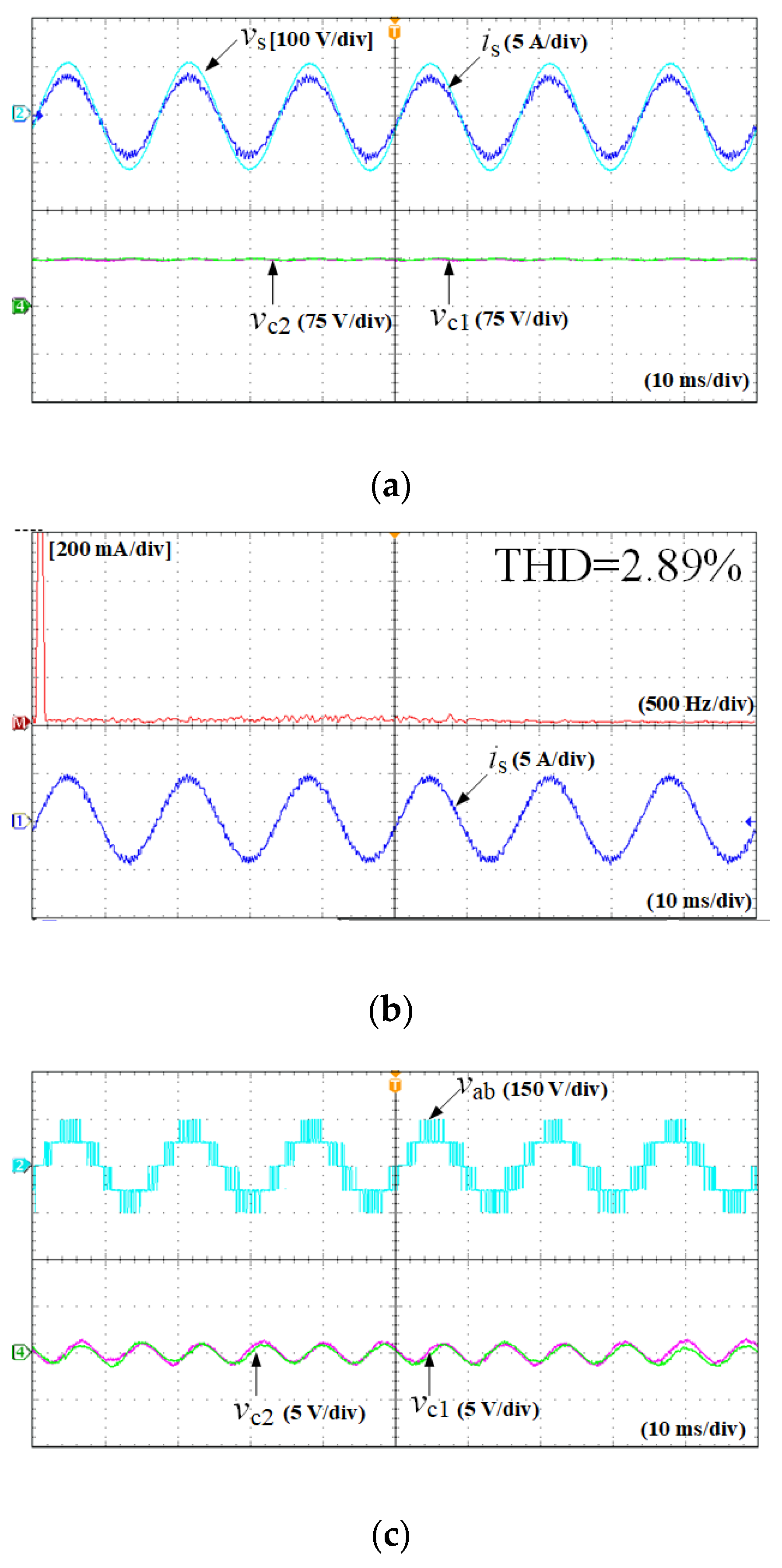
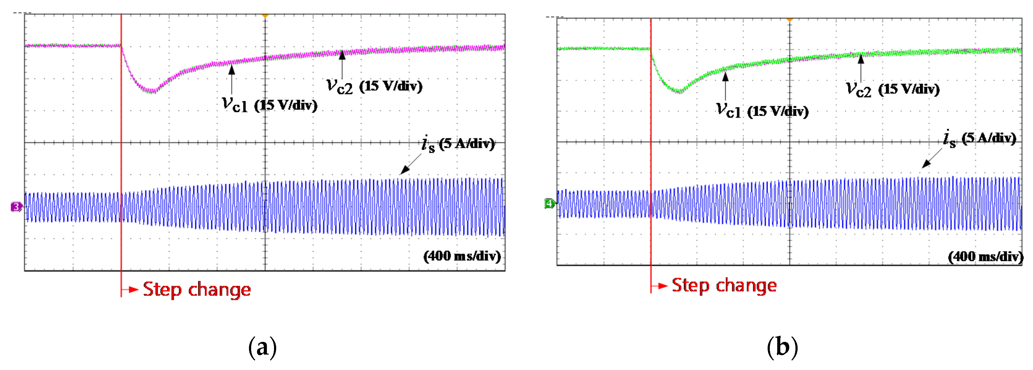
4. Experimental Results

The proposed method was tested with a prototype of the single-phase three-level NPC converter circuit. The peak value of the source line voltage was 110 V, the dc-link voltage was set to 150 V, and R L was 100 Ω. The proposed method and the conventional method for comparison were implemented on a digital signal processor (DSP) board TMS320F28335 (Texas Instruments Incorporated, Dallas, TX, USA). The sampling period T s was set to 50 µs to generate a sinusoidal ac source current with a unity power factor. Figure 7 shows the performance of the conventional MPC method as a function of different weighting factors. From Figure 7, the conventional MPC method in the experiment in this paper used the value 0.5 for the weighting factor.
The source voltage, source current, frequency spectra of the source current, line-to-line converter voltage, and the two capacitor voltages obtained by the conventional and proposed methods are shown in Figure 8 and Figure 9. It can be seen that the source currents are sinusoidal in phase with the source voltages and that the two capacitor voltages are well balanced for both methods. The frequency spectra of the source currents obtained from the conventional and proposed methods are also shown where it is evident that the total harmonic distortion (THD) of the proposed method is slightly lower than that of the conventional method. The converter input voltage and the two capacitor voltage waveforms obtained by the two methods are almost similar, as shown in Figure 8 and Figure 9. For the purposes of comparison, experimental results obtained by using only the difference-mode reference voltage without adding the common-mode voltage term are shown in Figure 10. It can be seen that the difference-mode reference voltage can synthesize sinusoidal source current even with a higher THD value as well as maintain the two capacitor voltages. In addition, the line-to-line converter input voltage exhibits only a three-level waveform with ± V d c and zero, as shown in Figure 10c. It can be seen that the model predictive control method with only the difference-mode voltage to control the grid currents can increase the current ripples, as shown in Figure 8 and Figure 10, because the limited number of the switching states are used. However, the proposed algorithm with both the difference-mode and the common-mode voltages results in reduced current ripples in comparison with the conventional method, as shown in Figure 8 and Figure 9.
In Figure 11a,b, experimental waveforms of the two capacitor voltages resulting from the conventional and the proposed methods are shown when intentionally imbalanced capacitor voltages occur. Both the conventional and proposed methods can balance the capacitor voltages with the almost same speed, as shown in Figure 11. Moreover, Figure 11c clearly illustrates that the NP voltage imbalance cannot be reduced if only the difference-mode reference voltage is used.
Figure 12 and Figure 13 show experimental waveforms of step changes of the load resistance from 200 Ω to 100 Ω and the dc load voltage from 150 V to 120 V obtained by the two methods. It is seen that the proposed method achieved dynamic responses as quickly as the conventional method.
Table 4 shows the calculation time of the conventional and the proposed methods to compare the computational complexity. The numbers of clocks of the conventional and the proposed methods were measured in the DSP board in the experimental setup and they were converted to the execution time required to perform the two control algorithms. As can be seen from Table 4, the proposed method yielded almost the same calculation time as the conventional method.
Table 5 summarizes the comparison between the conventional and proposed methods obtained by the above analysis and experimental results. Apparently, the proposed method did not require the tedious weighting factor selection procedure, which allowed time saving. The experimental results provided satisfactory performance under steady-state operation with slightly better source current THD and good capacitor voltages’ balancing. Additionally, the dynamic performance was guaranteed as fast as the conventional method. Meanwhile, the difference in computational time was negligible.

5. Conclusions

This paper proposes an MPC method for NPC converters to accomplish multiple objectives using single reference voltages without using a weighting factor in a cost function. The reference voltages in the proposed MPC algorithm consist of a difference-mode term and a common-mode term in each phase. The difference-mode term and the common-mode term are responsible for sinusoidal source current synthesis and capacitor voltage balancing, respectively. By simply comparing the single reference voltage with all possible voltage candidates producible in the single-phase three-level NPC converter, an optimal state for the dc voltage balance as well as the sinusoidal source current control with unity power factor can be selected at every step. As a result, the proposed method is free from the multi-objective optimization issues and the empirical approaches to selecting proper weighting factors that accompany conventional MPC methods for NPC converters. The proposed method is easy to implement since it has a deterministic approach for capacitor voltage balance as well as sinusoidal source current control, guaranteeing fast dynamic performance. The proposed method was verified experimentally for a single-phase three-level NPC converter.

Author Contributions

Conceptualization, S.K.; methodology, S.K. and E.-S.J.; software, E.-S.J.; validation, E.-S.J.; formal analysis, E.-S.J.; investigation, S.K. and E.-S.J.; resources, S.K.; data curation, E.-S.J. and M.N; writing—original draft preparation, E.-S.J. and M.H.N.; writing—review and editing, M.H.N.; visualization, E.-S.J.; supervision, S.K.; project administration, S.K.; funding acquisition, S.K. All authors have read and agreed to the published version of the manuscript.

Funding

This research was supported by the National Research Foundation of Korea (NRF) grant funded by the Korean government (MSIT) (2020R1A2C1013413).

Conflicts of Interest

The authors declare no conflict of interest.

References

  1. Kaźmierkowski, M.P.; Krishnan, R.; Blaabjerg, F. Control in Power Electronics: Selected Problems; Academic Press: Amsterdam, The Netherlands; New York, NY, USA, 2002; ISBN 9780080490786. [Google Scholar]
  2. Hill, R.J. Electric railway traction. Part 2: Traction drives with three-phase induction motors. Power Eng. J. 1994, 8, 143–152. [Google Scholar] [CrossRef]
  3. Steimel, A. Electric railway traction in Europe. IEEE Ind. Appl. Mag. 1996, 2, 6–17. [Google Scholar] [CrossRef]
  4. Takahashi, S.; Ogasawara, S.; Takemoto, M.; Orikawa, K.; Tamate, M. Common-Mode Voltage Attenuation of an Active Common-Mode Filter in a Motor Drive System Fed by a PWM Inverter. IEEE Trans. Ind. Applicat. 2019, 55, 2721–2730. [Google Scholar] [CrossRef]
  5. Jun, E.-S.; Park, S.; Kwak, S. Model Predictive Current Control Method with Improved Performances for Three-Phase Voltage Source Inverters. Electronics 2019, 8, 625. [Google Scholar] [CrossRef] [Green Version]
  6. Guzman, R.; de Vicuna, L.G.; Camacho, A.; Miret, J.; Rey, J.M. Receding-Horizon Model-Predictive Control for a Three-Phase VSI With an LCL Filter. IEEE Trans. Ind. Electron. 2019, 66, 6671–6680. [Google Scholar] [CrossRef] [Green Version]
  7. Mun, S.; Kwak, S. Reducing Common-Mode Voltage of Three-Phase VSIs using the Predictive Current Control Method based on Reference Voltage. J. Power Electron. 2015, 15, 712–720. [Google Scholar] [CrossRef]
  8. Fernão Pires, V.; Romero-Cadaval, E.; Vinnikov, D.; Roasto, I.; Martins, J.F. Power converter interfaces for electrochemical energy storage systems–A review. Energy Convers Manag. 2014, 86, 453–475. [Google Scholar] [CrossRef]
  9. Acuna, P.; Moran, L.; Rivera, M.; Aguilera, R.; Burgos, R.; Agelidis, V.G. A Single-Objective Predictive Control Method for a Multivariable Single-Phase Three-Level NPC Converter-Based Active Power Filter. IEEE Trans. Ind. Electron. 2015, 62, 4598–4607. [Google Scholar] [CrossRef]
  10. Habibullah, M.; Lu, D.D.-C.; Xiao, D.; Rahman, M.F. Finite-State Predictive Torque Control of Induction Motor Supplied From a Three-Level NPC Voltage Source Inverter. IEEE Trans. Power Electron. 2017, 32, 479–489. [Google Scholar] [CrossRef]
  11. Yaramasu, V.; Wu, B. Predictive Control of a Three-Level Boost Converter and an NPC Inverter for High-Power PMSG-Based Medium Voltage Wind Energy Conversion Systems. IEEE Trans. Power Electron. 2014, 29, 5308–5322. [Google Scholar] [CrossRef]
  12. Song, W.; Feng, X.; Smedley, K.M. A Carrier-Based PWM Strategy with the Offset Voltage Injection for Single-Phase Three-Level Neutral-Point-Clamped Converters. IEEE Trans. Power Electron. 2013, 28, 1083–1095. [Google Scholar] [CrossRef]
  13. Choi, U.-M.; Lee, H.-H.; Lee, K.-B. Simple Neutral-Point Voltage Control for Three-Level Inverters Using a Discontinuous Pulse Width Modulation. IEEE Trans. Energy Convers. 2013, 28, 434–443. [Google Scholar] [CrossRef]
  14. Tallam, R.M.; Naik, R.; Nondahl, T.A. A Carrier-Based PWM Scheme for Neutral-Point Voltage Balancing in Three-Level Inverters. IEEE Trans. Ind. Applicat. 2005, 41, 1734–1743. [Google Scholar] [CrossRef]
  15. de Freitas, I.S.; Bandeira, M.M.; de Macedo Barros, L.; Jacobina, C.B.; dos Santos, E.C.; Salvadori, F.; da Silva, S.A. A Carrier-Based PWM Technique for Capacitor Voltage Balancing of Single-Phase Three-Level Neutral-Point-Clamped Converters. IEEE Trans. Ind. Appl. 2015, 51, 3227–3235. [Google Scholar] [CrossRef]
  16. Wang, S.; Ge, X.; Xiong, C.; Song, W.; Feng, X. Single-phase three-level space vector pulse width modulation algorithm for grid-side railway traction converter and its relationship of carrier-based pulse width modulation. IET Electr. Syst. Transp. 2014, 4, 78–87. [Google Scholar] [CrossRef]
  17. Nabae, A.; Takahashi, I.; Akagi, H. A New Neutral-Point-Clamped PWM Inverter. IEEE Trans. Ind. Appl. 1981, IA-17, 518–523. [Google Scholar] [CrossRef]
  18. Lai, J.-S.; Peng, F.Z. Multilevel converters-a new breed of power converters. IEEE Trans. Ind. Appl. 1996, 32, 509–517. [Google Scholar] [CrossRef]
  19. Stala, R. Application of Balancing Circuit for DC-Link Voltages Balance in a Single-Phase Diode-Clamped Inverter with Two Three-Level Legs. IEEE Trans. Ind. Electron. 2011, 58, 4185–4195. [Google Scholar] [CrossRef]
  20. Habibullah, M.; Lu, D.D.-C.; Xiao, D.; Fletcher, J.E.; Rahman, M.F. Predictive Torque Control of Induction Motor Sensorless Drive Fed by a 3L-NPC Inverter. IEEE Trans. Ind. Inf. 2017, 13, 60–70. [Google Scholar] [CrossRef]
  21. Song, W.; Ma, J.; Zhou, L.; Feng, X. Deadbeat Predictive Power Control of Single-Phase Three-Level Neutral-Point-Clamped Converters Using Space-Vector Modulation for Electric Railway Traction. IEEE Trans. Power Electron. 2016, 31, 721–732. [Google Scholar] [CrossRef]
  22. Barros, J.D.; Silva, J.F. Optimal Predictive Control of Three-Phase NPC Multilevel Converter for Power Quality Applications. IEEE Trans. Ind. Electron. 2008, 55, 3670–3681. [Google Scholar] [CrossRef]
  23. Barros, J.D.; Silva, J.F.A.; Jesus, E.G.A. Fast-Predictive Optimal Control of NPC Multilevel Converters. IEEE Trans. Ind. Electron. 2013, 60, 619–627. [Google Scholar] [CrossRef]
  24. Scoltock, J.; Geyer, T.; Madawala, U.K. Model Predictive Direct Power Control for Grid-Connected NPC Converters. IEEE Trans. Ind. Electron. 2015, 62, 5319–5328. [Google Scholar] [CrossRef]
  25. Donoso, F.; Mora, A.; Cardenas, R.; Angulo, A.; Saez, D.; Rivera, M. Finite-Set Model-Predictive Control Strategies for a 3L-NPC Inverter Operating With Fixed Switching Frequency. IEEE Trans. Ind. Electron. 2018, 65, 3954–3965. [Google Scholar] [CrossRef]
  26. Calle-Prado, A.; Alepuz, S.; Bordonau, J.; Nicolas-Apruzzese, J.; Cortes, P.; Rodriguez, J. Model Predictive Current Control of Grid-Connected Neutral-Point-Clamped Converters to Meet Low-Voltage Ride-Through Requirements. IEEE Trans. Ind. Electron. 2015, 62, 1503–1514. [Google Scholar] [CrossRef] [Green Version]
  27. Jun, E.-S.; Kwak, S. A Highly Efficient Single-Phase Three-Level Neutral Point Clamped (NPC) Converter Based on Predictive Control with Reduced Number of Commutations. Energies 2018, 11, 3524. [Google Scholar] [CrossRef] [Green Version]
  28. Yang, Y.; Wen, H.; Fan, M.; Xie, M.; Chen, R. Fast Finite-Switching-State Model Predictive Control Method Without Weighting Factors for T-Type Three-Level Three-Phase Inverters. IEEE Trans. Ind. Inf. 2019, 15, 1298–1310. [Google Scholar] [CrossRef]
  29. Wu, W.; Wang, D.; Liu, L. A Multi-Layer Sequential Model Predictive Control of Three-Phase Two-Leg Seven-Level T-Type Nested Neutral Point Clamped Converter Without Weighting Factors. IEEE Access 2019, 7, 162735–162746. [Google Scholar] [CrossRef]
  30. Liu, X.; Qiu, L.; Fang, Y.; Ma, J.; Wu, W.; Peng, Z.; Wang, D. Lyapunov-based finite control-set model predictive control for nested neutral point-clamped converters without weighting factors. Int. J. Electr. Power Energy Syst. 2020, 121, 106071. [Google Scholar] [CrossRef]
  31. Jun, E.; Sangshin-Kwak; Baek, J. Model Predictive Control Method with NP Voltage Balance by Offset Voltage Injection for Single-phase NPC Converters. In Proceedings of the 2019 IEEE 28th International Symposium on Industrial Electronics (ISIE), Vancouver, BC, Canada, 12–14 June 2019; IEEE: Vancouver, BC, Canada, 2019; pp. 914–919. [Google Scholar]
  32. Jun, E.-S.; Nguyen, M.H.; Kwak, S. Three-Phase Three-Level Neutral Point Clamped Rectifier with Predictive Control Method without Employing Weighting Factor. Appl. Sci. 2020, 10, 5149. [Google Scholar] [CrossRef]
  33. Jun, E.-S.; Nguyen, M.H.; Kwak, S.-S. Model Predictive Control Method With NP Voltage Balance by Offset Voltage Injection for Three-Phase Three-Level NPC Inverter. IEEE Access 2020, 8, 172175–172195. [Google Scholar] [CrossRef]
  34. Kwak, S.; Park, J.-C. Predictive Control Method with Future Zero-Sequence Voltage to Reduce Switching Losses in Three-Phase Voltage Source Inverters. IEEE Trans. Power Electron. 2015, 30, 1558–1566. [Google Scholar] [CrossRef]
  35. Kim, J.-C.; Moon, S.-K.; Kwak, S. Direct model-based predictive control scheme without cost function for voltage source inverters with reduced common-mode voltage. Int. J. Electron. 2018, 105, 629–644. [Google Scholar] [CrossRef]
  36. Wang, S.; Song, W.; Ma, J.; Zhao, J.; Feng, X. Study on Comprehensive Analysis and Compensation for the Line Current Distortion in Single-Phase Three-Level NPC Converters. IEEE Trans. Ind. Electron. 2018, 65, 2199–2211. [Google Scholar] [CrossRef]
  37. Han, P.; He, X.; Ren, H.; Wang, Y.; Peng, X.; Shu, Z.; Gao, S.; Wang, Y.; Chen, Z. Fault Diagnosis and System Reconfiguration Strategy of Single-phase Three Level Neutral-Point-Clamped Cascaded Inverter. IEEE Trans. Ind. Appl. 2019, 55, 3863–3876. [Google Scholar] [CrossRef]
  38. Wang, S.; Song, W.; Zhao, J.; Feng, X. Hybrid single-carrier-based pulse width modulation scheme for single-phase three-level neutral-point-clamped grid-side converters in electric railway traction. IET Power Electron. 2016, 9, 2500–2509. [Google Scholar] [CrossRef]
  39. Lee, J.-S.; Kwak, R.; Lee, K.-B. Novel Discontinuous PWM Method for a Single-Phase Three-Level Neutral Point Clamped Inverter with Efficiency Improvement and Harmonic Reduction. IEEE Trans. Power Electron. 2018, 33, 9253–9266. [Google Scholar] [CrossRef]
Figure 1. Structure of single-phase NPC converter.
Applsci 10 08840 g001
Figure 2. Four possible situations depending on the location of the difference-mode reference voltages, leading to switching state of: (a) (1, −1); (b) (0, 0) with the a-phase reference voltage v d i f f a > 0 ; (c) (0, 0) with v d i f f a < 0 ; (d) (−1; 1).
Applsci 10 08840 g002
Figure 3. Possible locations of reference voltages in phase a and b ( v r e f a and v r e f b ) with a positive common-mode voltage ( v c o m m > 0 ) corresponding to Figure 2, leading to switching states: (a) (1, 0); (b) (1, 0); (c) (0, 1); (d) (0, 1).
Applsci 10 08840 g003
Figure 4. Possible locations of reference voltages ( v r e f a and v r e f b ) with a negative common-mode voltage ( v c o m m > 0 ) corresponding to Figure 2, leading to switching states: (a) (0, −1); (b) (0, −1); (c) (−1, 0); (d) (−1; 0).
Applsci 10 08840 g004
Figure 5. Control diagram of the proposed MPC method.
Applsci 10 08840 g005
Figure 6. A flow chart of the proposed MPC method.
Applsci 10 08840 g006
Figure 7. The THD of the source current and peak-to-peak value of the capacitor ripple voltage obtained by the conventional MPC method vs. weighting factor ( λ c ).
Applsci 10 08840 g007
Figure 8. Experimental results from the conventional method: (a) source voltage ( v s ) , source current ( i s ), capacitor voltages ( v c 1 and v c 2 ); (b) fast Fourier transform (FFT) spectrum of source current ( i s ); and (c) line-to-line converter voltage ( v a b ) and ac component of capacitor voltages ( v c 1 and v c 2 ).
Applsci 10 08840 g008
Figure 9. Experimental results from the proposed method: (a) source voltage ( v s ) , source current ( i s ), capacitor voltages ( v c 1 and v c 2 ); (b) FFT spectrum of source current ( i s ); and (c) line-to-line converter voltage ( v a b ) and ac component of capacitor voltages ( v c 1 and v c 2 ).
Applsci 10 08840 g009
Figure 10. Experimental results using only the difference-mode reference voltage without the common-mode voltage terms: (a) source voltage ( v s ) , source current ( i s ), capacitor voltages ( v c 1 and v c 2 ); (b) FFT spectrum of source current ( i s ); and (c) line-to-line converter voltage ( v a b ) and ac component of capacitor voltages ( v c 1 and v c 2 ).
Applsci 10 08840 g010
Figure 11. Experimental results for capacitor voltages’ ( v c 1 and v c 2 ) correction from an unbalanced voltage condition obtained by: (a) the conventional method; (b) the proposed method; and (c) using only the difference-mode reference voltage without the common-mode voltage term.
Applsci 10 08840 g011
Figure 12. Experimental results for capacitor voltages ( v c 1 and v c 2 ) and source current ( i s ) with a step change of the load resistor from 200 Ω to 100 Ω obtained by: (a) the conventional method; (b) the proposed method.
Applsci 10 08840 g012
Figure 13. Experimental results for capacitor voltages ( v c 1 and v c 2 ) and source current ( i s ) with a step change of dc voltage from 150 V to 120 V obtained by: (a) the conventional method; (b) the proposed method.
Applsci 10 08840 g013
Table 1. Units for magnetic properties.
#Operating StatusSwitching StateInput VoltageCapacitor Voltage
S a S b S a 1 S a 2 S b 1 S b 2 v a b v c 1 v c 2
100OFFONOFFON0--
211ONONONON0--
3−1−1OFFOFFOFFOFF0--
41−1ONONOFFOFF V d c
510ONONOFFON V d c / 2
60−1OFFONOFFOFF V d c / 2
701OFFONONON V d c / 2
8−10OFFOFFOFFON V d c / 2
9−11OFFOFFONON V d c
# items number.
Table 2. Polarity relationship among switching states, a-phase difference-mode reference voltage, and the common-mode voltage.
S a S b S p o l y v d i f f a v c o m m
101(+)(+)
−101(−)(−)
01−1(−)(+)
0−1−1(+)(−)
Table 3. Offset voltage to be injected to decrease the difference between two capacitor voltages at the next step.
v c ( g a p ) v d i f f a i s v c o m m
v c ( g a p ) 0 v d i f f a 0 i s 0 v d i f f a V d c 2
i s < 0 v d i f f a + V d c 2
v d i f f a < 0 i s 0 v d i f f a + V d c 2
i s < 0 v d i f f a V d c 2
v c ( g a p ) < 0 v d i f f a 0 i s 0 v d i f f a + V d c 2
i s < 0 v d i f f a V d c 2
v d i f f a < 0 i s 0 v d i f f a V d c 2
i s < 0 v d i f f a + V d c 2
Table 4. Computational complexity comparison between the conventional and proposed methods.
Conventional MethodProposed Method
Computational time (µs)5.2625.263
Table 5. Summarized comparison between the conventional and proposed methods.
CriteriaConventional MethodProposed Method
Weighting Factor Tuning ProcedureYesNo
Steady-state performanceSource current THD (%)2.992.89
(slightly better)
Capacitor voltage balancingGoodGood
Transient-state performanceCapacitor voltages balancing speedFastFast
Reference trackingFastFast
OvershootNoNo
Computational time (µs)5.2625.263
Publisher’s Note: MDPI stays neutral with regard to jurisdictional claims in published maps and institutional affiliations.

