1. Introduction
In current photonic networks, wavelength-division multiplexing (WDM), in which optical signals with different wavelengths are combined into one optical fiber and separated after transmission, is essential for large network capacity. Since its invention around 1980, the arrayed waveguide grating (AWG) has been globally applied for WDM as a wavelength multiplexer and demultiplexer [
1,
2,
3]. AWGs have highly contributed to telecommunications growth in line with the progress in silica-based planar lightwave circuits (PLCs), which have other applications such as optical splitters, switches, and attenuators [
4].
Figure 1a illustrates the configuration of an AWG, which is compared with the conventional prism-type spectrometer. The AWG is composed of input waveguides, an input slab waveguide, arrayed waveguides, an output slab waveguide, and output waveguides. The configuration and function are the same as that of the prism-type spectrometer. The arrayed waveguides correspond to a prism as a dispersive medium, and the input/output slabs correspond to collimating and focusing lenses. The AWG features compactness and uniform insertion loss owing to its wafer-process fabrication. A silica AWG on silicon or silica substrate has further benefits, including low loss, compatibility with silica-based optical fiber compared with other materials, an easily scalable and customizable channel number and spectral shape, cost-effective mass productivity, and high reliability under various mechanical and environmental conditions. There are a variety of AWGs with respect to their channel number, spacing, and so on. In the early 2000s, when Internet usage surged rapidly, a record large number of 400 channels and narrow spacing of 1 GHz were reported [
5,
6]. Currently, the International Telecommunication Union (ITU) has standardized several channel spacing options, such as 12.5, 50, and 100 GHz [
7]. A WDM system with less than 200-GHz spacing is called dense WDM (DWDM), which is widely used in commercial long-haul and metro networks. For example, 40 channels with 100-GHz spacing in the 1.5-μm wavelength band (C-band) is one of the common allocations. In regards to other AWG characteristics, temperature compensation or athermalization have been adopted [
8,
9]. Methods for reducing crosstalk between channels have also been reported [
10]. Another essential characteristic is flat-top shaping, which will be covered in the next section in detail.
Long-haul traffic has grown owing to the contribution of AWGs in DWDM line-side networks. However, data traffic in shorter reaches is becoming more and more important recently. The global trend in data traffic is summarized in
Figure 1b. The solid line (black) represents data traffic on a logarithmic scale [
11]. Since the remarkable increase after the millennium, traffic has continuously increased and will reach petabits per second soon after 2020. In the meantime, client-side interfaces have also progressed exponentially. The triangles and dashed line (blue) are the standardization year and extrapolated Ethernet growth, respectively, which indicate that Ethernet speed has increased by a factor of ten within about a seven-year period. The 100-gigabit Ethernet (100 GbE) and beyond have been standardized since 2010. Based on current technology trends, client-side networks such as those used in datacenters and for mobile links with the reach of 100 km or less will consume more data for local wireless traffic with the advent of self-driving vehicles, edge computing for artificial intelligence, and automation with the Internet-of-Things (IoTs). These developments will require real-time operation without latency, ensured security, and event-driven data processing. Accordingly, future networks should not only be cloud storage-based but also have distributed computing edges to accommodate a variety of data protocols other than TCP/IP. Toward the realization of such data-centric communications and computing, photonics technology will play a more important role in overcoming electronic limitations on operating frequency and power consumption, referred to as Moore’s law [
12]. In particular, wavelength scalability and functionality through multi-wavelength integrated devices will be a key to promoting the spread of future innovative all-photonic networks [
13].
Here, we review our research and development of receivers integrated with an AWG for WDM toward the data-centric era. Among the various merits of the AWG, we focus on its low-loss and flat-top functions. The receivers feature a multimode-output AWG (MM-AWG), which is a low-loss flat-top WDM filter. The milestones of our work are plotted by circles (red) in
Figure 1b.
Section 2 describes the basic design of the MM-AWG and covers another essential factor, namely optical coupling between multimode output and a photodiode (PD). In later sections, we describe our WDM photoreceivers for 10, 40, and 100 Gb/s and beyond in detail [
14,
15,
16,
17,
18,
19,
20,
21] along with recent progress on 400-Gb/s transmission.
Section 6 summarizes the paper.
2. MM-AWG and Optical Coupling
Insertion loss and transmission bandwidth are the essential parameters in AWG design. In general, both are apt to be in a trade-off relationship. For example, parabola shaping is a simple solution to increase bandwidth by adding a taper structure at slab waveguides, though the loss increases [
22]. To overcome the tradeoff, synchronic configurations have been proposed [
23,
24], which consist of a cascading Mach-Zehnder interferometer (MZI) and AWG that provide low loss and a wide-band filter shape. This is a sophisticated approach, however, requiring high process uniformity for phase matching and a large chip for the cascading layout. Therefore, those types of AWGs have mainly been applied for high-spec networks with a large number of channels.
As mentioned before, WDM is more important in client-side optics. Currently, for instance, WDM-based Ethernet specifications have already been standardized for 40 and 100 Gb/s and beyond [
25,
26]. As the client-side demultiplexer, free-space optics with thin-film filters (TFFs) has been used, especially in coarse WDM (CWDM) systems with a small number of wavelengths [
27,
28]. However, this optics has drawbacks. One is the need for complex and precise assembly in building an optical block using TFFs and collimating lenses. Furthermore, it is more difficult to configure for denser or larger-scale WDM. Hence, an alternative demultiplexer based on a PLC is a very promising candidate, which has also been widely implemented in optical transceivers. In our study, we used the MM-AWG, a low-loss flat-top demultiplexer, to build WDM photoreceivers with total bit rates of 10, 40, 100 Gb/s, and beyond.
In contrast to the conventional AWG with single-mode output waveguides, the MM-AWG with multimode output waveguides provides a flat-top passband with low loss [
29,
30]. We describe the procedure for estimating the spectral shape of MM-AWG using
Figure 2. The design condition exemplified here is based on a silica PLC for the 1.3-μm band with an index difference between the core and cladding of 2%, which is utilized in our 100-Gb/s photoreceiver (described later in
Section 5). First, as shown in
Figure 2a, the effective index of a waveguide is calculated as function of waveguide width. A vector finite difference mode solver was used to estimate the effective index in each mode order [
31]. Parameter
m is the mode order. The more the width of the output waveguides is enlarged, the higher the modes that are generated. In this case, a total of six modes, including the fundamental one (
m = 0), exist within the waveguide width of 15 μm. Second, as shown in
Figure 2b, the spectral shapes of the AWG are calculated for each mode and combined. The spectral flatness is determined by the number of modes taken into account, or by the waveguide width. The more modes taken into account, the flatter the spectral shape becomes, together with a reduction of insertion loss.
Here, we explain the layout design and typical spectrum of the MM-AWG. The design condition is based on a silica PLC for the 1.5-μm band, which is used in our 10-Gb/s receiver (presented in the next section).
Figure 3a shows a schematic of the design of the AWG chip and a cross-sectional view of the waveguide. This silica-based MM-AWG has eight output ports consisting of single-mode-input and multimode-output waveguides. All the output channels are designed on the CWDM grid with the channel spacing of 20 nm. The MM-AWG has a gull-wing shape, and the chip size is 11 mm × 65 mm, using the index difference of 0.75%. The core sizes of the input and output waveguides are 6 × 6 and 6 × 30 μm, respectively. Note that the chip size is dependent on the index difference. Since the curvature or bending radius decreases as the index difference increases, the AWG layout shrinks and the chip size decreases for larger index differences. In addition, core size also depends on the index difference. A higher index provides a smaller core. For optical coupling between single-mode PLC waveguide and standard single-mode fiber with core size from 8 to 10 μm, the optimal index difference in our PLC to minimize coupling loss is about 0.5%. The transmission spectrum of a fabricated MM-AWG is shown in
Figure 3b. The insertion loss of the MM-AWG is as low, as less than 1 dB in each passband when multimode fiber is connected to the output port of the AWG. The 0.5-dB bandwidth is larger than 13 nm, which corresponds to channel spacing as wide as 65%.
The demultiplexed multimode optical signal is not appropriate for retransmission through a single-mode optical fiber due to the loss of higher modes. Therefore, a photoreceiver in which the multimode signal is instantly converted into electric signal should be used. However, even if the spectral shape is flat at the output of the MM-AWG, poor coupling with PDs degrades the shape. Next, we need to design the optical coupling between the multimode output of the MM-AWG and the PD.
The output beam from a multimode waveguide can be approximated by combining higher-order Gaussian beams. The electric field radiated from a waveguide,
, is represented as:
where
and
are the electric field and beam waist (spot size) at the waveguide edge, respectively, and
is a Hermite polynomial of
m order. Here,
,
, and
are defined as:
From the above Equations, coupling efficiency between the electric field of the MM-AWG output and PD are estimated.
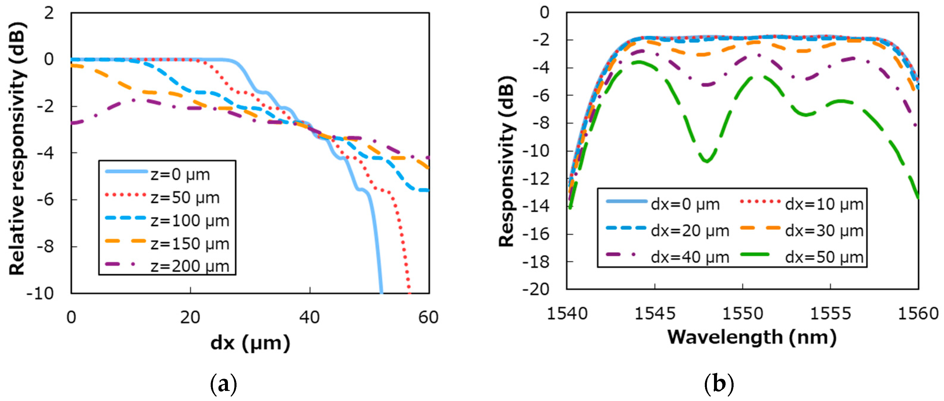
Figure 4a shows the calculated relative responsivity of optical coupling for the highest mode. The design condition is based on a silica PLC for the 1.5-μm band with the index difference of 0.75%. Here,
z is the distance between the edge of the MM-AWG output and the PD surface, and
dx represents displacement from the center. The diameter of the PD is assumed to be 80 μm. Since the beam output from the MM-AWG creates complicated speckle patterns that can be mixed by fundamental and higher modes, a sufficiently large detection area of the PD is required to capture all the modes. We consider the following conditions:
dx and
z are small enough to obtain flat responsivity but large enough for alignment and tolerance to assembly error. The diameter of the PD should be large enough to provide flat responsivity but small enough to obtain high-speed operation. This plot reveals that received intensity degrades depending on both
z and
dx. The degradation of 1 dB occurs at
dx ~20 μm for
z = 100 μm and at
dx ~10 μm for
z = 150 μm.
Figure 4b shows measured spectral shapes coupled by MM-AWG and PD, which depend on offset
dx at
z = 150 μm. The results clearly show that the shape distorts and responsivity degrades when misalignment increases. Whereas the calculation in
Figure 4a is only for one of the modes (
m = 6), the shapes in
Figure 4b include all the coupled modes. In this condition, the assembly tolerance is within ±30 μm for 1-dB degradation of responsivity. With these design guidelines, we succeeded in developing high-speed photoreceivers.
3. Receiver Integration for WDM with 10-Gb/s Throughput
Here, we describe our photoreceiver integrated with the MM-AWG for 10-Gb/s throughput. The reason for applying WDM for such a “low speed” is that dividing the bitrate per channel, or reducing the baud rate, provides three merits. First, it enables us to use a PD with a large receiving diameter, which relaxes the assembly tolerance required to maintain minimum coupling loss between higher-mode beams and PD. Second, a lower baud rate is more suitable for longer reaches in terms of the dispersion penalty and noise figure. In addition, the link margin or distance can be further improved by using an avalanche photodiode (APD), which, theoretically, provides more than 100 times the gain of the conventional PD [
32]. Third, cost-effective parts are available for electrical circuits and boards, as well as optical components operating in the 1.5-μm band, or C-band. The use of CWDM is another option to relax the specifications of those components. We chose eight-wavelength CDWM with 20-nm channel spacing with the baud rate of 1.25 Gb/s [
14].
Figure 5a is a schematic of the configuration of the integrated 10-Gb/s CWDM photoreceiver. It is composed of an MM-AWG, a PD array attached to a ceramic carrier, a circuit board including transimpedance amplifiers (TIAs), and a sub-mount. A pigtail fiber is connected to the input edge of the AWG. For hybrid integration with the MM-AWG and the PD array, we used mechanical alignment. The sub-mount, which serves as an alignment platform, is made with machining accuracy of better than 10 μm. On the sub-mount (inset), several grooves are formed and filled with bonding adhesive in assembly. Owing to the tensile strain induced by the adhesive spreading in the grooves while curing, high mounting accuracy for the MM-AWG and PD array of better than 5 μm is provided. Therefore, the total alignment error in this mechanical alignment is less than 15 μm.
A photograph of the fabricated photoreceiver is shown in
Figure 5b. The MM-AWG was fixed at the center of the aluminum sub-mount. A circuit board with TIAs was also mounted on the sub-mount. The eight-channel silica-based MM-AWG had the index difference between the core and cladding of 0.75%, and the cores of the input and output waveguides are 6 × 6 and 6 × 30 μm in size, respectively. The eight-channel PD array consists of InGaAs pin-PDs on a ceramic carrier. Each PD has a responsivity of over 1 A/W. The signal output from the PD array was fed into electrical transmission lines on the ceramic carrier followed by the TIAs via bonding wires. The size of the package is 100 × 50 mm.
The responsivity spectra of the photoreceiver shown in
Figure 5c indicate that we obtained a high, flat-top responsivity for all channels. Within each passband of 13 nm, the responsivity ranges from 0.7 to 0.85 A/W. The crosstalk level is better than −22 dB. The polarization-dependent loss is 0.2 dB or less at the center wavelength of the grid, which is the same as that of the MM-AWG itself. The coupling loss between the input fiber and the PD is estimated at 1 dB, the same as in the fiber-coupled measurement; therefore, there is almost no degradation due to optical coupling by mechanical alignment.
As shown in
Figure 5d, we also measured the bit-error-rate (BER) characteristics when all the channels were driven simultaneously. The experimental setup is shown on the left. The signal from the pulse-pattern generator (PPG) was a 1.25-Gb/s non-return-to-zero (NRZ) 2
7-1 pseudo-random bit sequence (PRBS). The WDM signal generated from 10-Gb/s transmitters and a coupler was transmitted in a single-mode fiber with back-to-back connection and fed into the photoreceiver while input power was changed by the valuable optical attenuator (VOA). The BER of the photoreceiver was measured by clock-and-data recovery (CDR) followed by an error detector (ED). We observed error-free transmission with the minimum receiver sensitivity from −24 to −20 dBm at a rate of 10
−11. Since the sensitivity tends to degrade in edge channels such as channel 1 and 8, the layout of transmission lines and electrical components on the circuit board should be optimized for further reduction of the sensitivity deviation.
4. Receiver Integration for WDM with 40-Gb/s Throughput
The second photoreceiver we developed operates at higher speeds and is more compact than the previous one. One option to scale up from 10 to 40 Gb/s is just to increase the number of wavelengths; however, a configuration with a few tens of wavelengths for DWDM is not appropriate in terms of compactness and cost-effectiveness. To decrease the number of wavelengths, or increase baud rate per channel, we necessarily consider not only higher-speed operation but also the dispersion penalty and electrical crosstalk. Regarding dispersion, we choose the 1.3-μm wavelength band, the so-called O-band, which mitigates the penalty compared with that in the C-band. As for electrical crosstalk, we applied a fan-out design in a PLC circuit to enhance electrical isolation as much as possible. Here, we referred to a specification from the Very Short Reach (VSR) interface for 40-Gb/s, allocated in the Optical Internetworking Forum, which is called VSR-5 [
33]. The channel number is four, with wavelength spacing of 24.5 nm, which is slightly wider than the 20-nm spacing of CWDM with the baud rate of around 10 Gb/s [
15].
Figure 6a is a schematic view of our integrated photoreceiver. It comprises a MM-AWG PLC, a fan-out PLC, and an electrical circuit including TIAs. The PLC of the AWG and the fan-out PLC are separated chips bonded by adhesive with high optical transparency. Such a dual-PLC structure enables us to optimize the two PLCs separately in terms of yield and size. On the fan-out PLC, edge-illuminating PDs are flip-chip bonded. For assembly with higher accuracy than that with 10-Gb/s photoreceiver, we used visual alignment. The inset illustrates the hybrid integration of the PDs on the fan-out PLC. The alignment is performed visually using markers on the PD and PLC, and the assembly error is less than 1 μm [
4]. Designing the fan-out so that the channels are separated can suppress electrical inter-channel crosstalk. According to our estimation from RF simulation, separation over 1.5 mm provides electrical isolation of more than 20 dB at the frequency of 10 GHz.
Photographs of the fabricated photoreceiver are shown in
Figure 6b. The MM-AWG bonded with the fan-out PLC and circuit board are mounted in a package. The enlarged photograph shows the InGaAs PD, which is hybridly integrated on the fan-out PLC, connected to TIA via electrical wire. The index difference between the core and cladding was 1.5%. The measured 3-dB-down bandwidth of the receiver was larger than 9 GHz, and the adjacent crosstalk was better than 21 dB, as we estimated. The size of the small and compact package is 64 × 25 mm.
Figure 6c shows the responsivity spectrum of the receiver. For all channels, a high responsivity of about 0.4 A/W was observed. While there is some degradation of flatness because of the loss of higher modes in the optical coupling, the responsivity shows that high assembly accuracy was achieved.
The BER characteristics of the 4 × 10-Gb/s receiver are shown in
Figure 6d. The experimental setup is shown on the left. Each 10-Gb/s signal was input into a 40-Gb/s transmitter, which we also fabricated. The transmission length of the fiber was 5 km. When all the channels were driven simultaneously, error-free transmission was successfully achieved with a receiver sensitivity of less than −12 dBm. The sensitivity degradation was less than 1.5 dB compared with a single-channel drive. The results indicate that the inter-channel crosstalk was sufficiently suppressed by using the fan-out PLC.
5. Receiver Integration for WDM with Throughput by 100-Gb/s and beyond
The third WDM photoreceiver has the baud rate of 25 Gb/s. Here, we mainly describe the receiver with throughput of 100 Gb/s by four-channel WDM. Moreover, our basic design can leverage beyond 100 Gb/s, such as 200 and 400 Gb/s. Using a low-loss MM-AWG with a higher index difference as well as highly accurate assembly with lensed optical coupling, we were able to develop a compact photoreceiver [
16]. We referred to IEEE’s standard for transceivers for Ethernet 100 GbE [
25] and multi-source agreements (MAs), which stipulate that the size of the transceiver should have a size, or form factor, that can be accommodated in the restricted rack space in datacenters. For the transmission reach of 10 and 40 km, a 4-channel WDM should be used with a 25-Gb/s NRZ signal for each channel. The wavelength allocation is called LAN-WDM, which is in the 1.3-μm band, and the grid spacing is 800 GHz with the passband of 360 GHz. This is one of the best allocations for a lower dispersion penalty than in CDWM as well as for more cost-effective components than in DWDM.
Figure 7a illustrates the core assembly of 100-Gb/s LAN-WDM photoreceiver, which is composed of an MM-AWG, a collimating lens, a focusing lens array, and a PD array, all bonded as a single assembly block. The four-channel InGaAs PD array is mounted on a ceramic carrier by flip-chip bonding for back illumination. Between the MM-AWG and PD array, the focusing lens array based on a graded-index (GRIN) micro lens is fixed to the edge of the output waveguides. On the input side, the beam-collimating lens is directly attached to the MM-AWG. For all the optical connection in the core assembly, we used an active alignment technique. It provides very high accuracy alignment by way of inputting an optical signal into each component. The assembly configuration between the PLC and PD array is the same as that in our integrated coherent receiver [
34], while the main difference is that the multimode beam from the MM-AWG is coupled with the PDs by a dedicated optical design. For both optical coupling to the multimode beam and high-speed operation, we use a racetrack shape in the PD active region.
A photograph of the fabricated photoreceiver is shown in
Figure 7b along with a photograph of the footprint of the Ethernet transceiver. Viewed from the outside, the receiver consists of a metal hermetically sealed package, a receptacle LC connector with another focusing lens, and flexible printed circuits (FPCs). The core assembly including the AWG and PDs is mounted in the package together with a four-channel TIA on a circuit board. The MM-AWG was fabricated with index difference of 2% with the core width of 5 μm for single-mode input and 15 μm for multimode output. The receiver can be applied for a reach of 10 km by using pin-PD. Furthermore, the reach can be extended by replacing the pin-PD with an APD [
35]. The size of the package is 7 × 18 × 6 mm
3, excluding the receptacle and FPCs, which is small enough to install it in compact transceivers such as QSFP-DD and OSFP [
36,
37].
Figure 7c shows the responsivity spectrum of our fabricated photoreceiver. A flat-top spectral shape of over 500 GHz was observed, and the maximum responsivity reached higher than 0.7 A/W for all channels. The total optical loss is about 1.5 dB, which includes 0.8-dB AWG loss, 0.3-dB coupling loss from PLC to PD, and 0.3-dB loss from PLC to receptacle. The crosstalk between adjacent channels is less than 25 dB in the 360-GHz passband. In addition to performing measurements at room temperature, we also conducted environmental tests, such as temperature tracking from 5 to 80 °C and high-temperature storage at 85 °C. Mechanical vibration and shock were also investigated. In all the tests, we confirmed the loss change as low as less than 0.2 dB, which reveals the high reliability of the photoreceiver owing to our stable core assembly structure.
Figure 7d shows the measured BER characteristics of the 100-Gb/s pin-PD photoreceiver. The 4 × 25 Gb/s NRZ signals were input into a 100-Gb/s transmitter we also fabricated [
38]. After 10-km fiber transmission, the WDM signal was detected at our receiver while input power was changed by a VOA. The BER of the photoreceiver was measured by CDR and an ED. As a result, we obtained the minimum receiver sensitivity of less than −10.9 dBm in optical modulation amplitude (OMA) at a BER = 10
−12. As compared with back-to-back (BtoB) transmission, we also confirmed that the crosstalk penalty was negligible. These results can satisfy the specifications for 10-km 100 GbE links with a sensitivity margin of over 4 dB even though the photoreceiver is based on a pin-PD. By replacing the pin-PD with an APD, we confirmed further extended reach of 40 km.
We have used our photoreceiver design concept in developing several types of other photoreceivers and aggregating configurations. For example, ramping up to 200-Gb/s throughput was achieved by adopting four-level pulse-amplitude modulation (PAM4) [
18]. In addition, we have also developed a 400-Gb/s photoreceiver using eight-channel WDM together with the PAM4 format [
21]. Moreover, we have demonstrated 400-Gb/s aggregations of 16 λ × 25-Gb/s NRZ and 8 λ × 50-Gb/s PAM4 signals by using the 100GbE devices and functional cyclic AWGs [
19,
20]. Furthermore, we have recently reported 400-Gb/s transmission with 4 × 100-Gbit/s/λ WDM photoreceivers [
39,
40,
41]. These consecutive studies have clearly shown our receiver integration technology is very promising for current networks as well as for future data-centric architectures.

 ,
, 


