Abstract
We report on the microelectronic characteristics of a novel hybrid heterojunction device based on a solution processable semiconducting polymer poly(9,9-dioctylfluorenyl-2,7-diyl)- co-(N,N0-diphenyl)-N,N′di(p-butyl-oxy-pheyl)-1,4-diamino-benzene) (PFB) and p-type silicon (p-Si). The PFB/p-Si heterojunction is prepared by spin coating 20 mg/mL solution of PFB in chloroform on the precleaned polished surface of p-Si substrate. Thermal evaporation of silver (Ag) electrode on top of PFB completes the fabrication of the Ag (90 nm)/PFB (180 nm)/p-Si heterojunction device. Morphology of PFB thin film is studied by using an atomic force microscope (AFM) and scanning electron microscope (SEM), which reveals grains are randomly distributed with slightly different grain sizes and shapes. It leads the film to form nonuniformity and some roughness in its topography that results in limiting the current (I) flow across the film/interface with p-Si. Ultraviolet (UV–vis) absorption and X-ray diffraction (XRD) spectra are measured for optical bandgap and crystal structure analysis of PFB. The key microelectronic parameters—rectification ratio (RR), ideality factor (n), barrier height (Φb), series resistance (Rs) and reverse saturation current (I0)—of the Ag/PFB/p-Si heterojunction are found from current–voltage (I–V) characteristics at room temperature (300 K) in dark conditions (≈0 lux). The Ag/PFB/p-Si heterojunction device exhibits improved microelectronic parameters when compared to those of earlier reported devices that were prepared in the same configuration. This improvement in the device parameters reveals enhancement in the microelectronic properties across the interface/depletion region of the Ag/PFB/p-Si device, which can be attributed to the remarkable electronic properties of PFB such as its relatively high hole mobility and better charge carriers’ conduction. The charge transport mechanisms through the device is also studied. Having the smaller values of I0 ≈ 7 × 10⁻¹⁰ A and n ≈ 3.23, as well as higher shunt resistance (Rsh) of 32 GΩ for the Ag/PFB/p-Si device suggest its potential for many electronic and optoelectronic applications.
1. Introduction
Organic semiconductors are one of the most favorable emerging materials for their possible applications in electronic, optoelectronic, thermoelectric, and photonic devices [1,2,3,4,5]. For instance, these materials have been successfully employed in organic light emitting diodes (OLEDs), organic field effect transistors (OFETs), organic photovoltaics (OPVs), and organic solid-state lasers [6,7,8,9]. Organic semiconductors possess exciting electrical and optoelectronic properties due to its pi (π)-conjugated molecular structure that permits the conduction of charge carriers through a hopping process [10]. They offer several distinct properties of their kind, which include mechanical flexibility, solubility in various organic solvents, easy processing for device fabrication (spin coating, drop casting, inkjet printing, etc.), chemical as well as thermal stabilities, and relatively low-cost, when compared to inorganic semiconductors [11,12]. In light of the aforementioned properties, it is believed that in near future, organic semiconductors may replace the existing technology of inorganic semiconductors, which are more expensive and require complicated procedures at high temperatures for device fabrication [13].
Organic semiconducting materials can be found either as small molecules, oligomers, or polymers. Particularly, polymeric semiconductors have the advantage that they are generally soluble in different solvents, which makes them suitable for easy device fabrication via spin coating and drop casting. Amongst a large number of semiconducting polymers, poly-(9,9-dioctylfluorenyl- 2,7-diyl)-co-(N,N0-diphenyl)-N,N′di(p-butyl-oxy-pheyl)-1,4-diamino-benzene) (PFB) is one of the best semiconducting materials that has relatively higher hole mobility due to its large π-conjugated structure, as well as good chemical and thermal stabilities [14]. PFB has found its applications in OLEDs and OPVs due to its high photoluminescence, fluorescence, and strong absorption with broad band in the UV–vis spectrum [15,16]. However, at the microscopic level, the microelectronic properties of PFB thin films at the junction/interface with other semiconducting materials still need to be studied, understood, and tuned for improvements.
Interfaces and junctions between different semiconductors and/or metals play a pivotal role, like a building block in semiconductor devices [17,18] such as PV cells [19,20], FET [21], and photo detectors [18]. A hybrid organic–inorganic heterojunction device is fabricated by forming a thin organic semiconductor layer on an inorganic semiconductor, which behaves as a rectifying junction [22]. The structure of the hybrid organic–inorganic heterojunction is of great importance due to the fact that it utilizes the higher charge carrier mobility of an inorganic semiconductor and its solution processing ability, as well as the easy fabrication process of organic semiconductor thin films for device fabrication. These hybrid heterojunctions also provide an excellent platform for wide-range and superior applications by employing desired organic materials that possess interesting optoelectronic properties, remarkable scalability, and high flexibility. Organic materials in heterojunction devices with inorganic semiconductors manifest fabrication at low temperature by simple cost-effective deposition techniques [23]. Although the benefits and significance of organic heterojunction are sufficiently vast, the complete understanding about their properties still remains an issue of discussion.
Herein, we study the microelectronic properties of the Ag/PFB/p-Si heterojunction to explore and understand the junction parameters for its potential applications in electronic and optoelectronic devices such as OPVs and organic–inorganic hybrid sensors. Current–voltage (I–V) characteristics of the device are studied by using the conventional I–V method and Norde’s functions for comparison of microelectronic parameters. Furthermore, the morphological, structural, and optical properties are also studied to understand surface features, crystallinity, and bandgap of the PFB thin films.
2. Experimental Work
The polished surface of p-Si wafer (100) obtained from Sigma Aldrich was used as a substrate. The substrate was treated with HF:H2O to etch the top oxide layer from Si. It was then cleaned in ultrasonic bath with acetone and isopropanol for 5 min in each. A uniform solution of PFB was prepared in chloroform at 20 mg/mL with the help of a magnetic stirrer at room temperature (300 K). The solution was spin coated on p-Si substrate at 3000 rpm for 20 s. Then, the sample was allowed to dry at 60 °C by using a hot plate for 1 h under nitrogen gas flow. A 90 nm-thick layer of silver (Ag) electrode was thermally deposited on PFB via a vacuum thermal evaporator at 1.5 × 10⁻⁵ mbar to make the sandwich-type Ag/PFB/p-Si heterojunction device. The current–voltage (I–V) characteristics were performed to extract different device parameters. Additionally, morphology of the PFB thin film was investigated by using an atomic force microscope (AFM) NanoScope-IIIa SPM from Dimension TM 3100, Digital Instruments Veeco Metrology Group, which was operated in noncontact mode to avoid any damage to the film. The scan area was 2 μm × 2 μm while the scan rate was kept as low as 0.86 Hz to see detailed surface features. Scanning electron microscopy (SEM) JEOL JSM-840 was also carried out to correlate with the AFM images. A two-dimensional SEM image on 2.5 μm × 2.5 μm scale was recorded at 50,000× magnification operated at 15 kV. The spectroscopic studies of PFB were carried out via ultraviolet and visible (UV–vis) UV/Vis/NIR spectrophotometer LAMBDA 950 PerkinElmer and Fourier transform infrared (FT-IR) IR Tracer-100 FTIR Spectrometer (Shimadzu). The crystallinity of PFB was investigated by using X-ray diffraction (XRD) with a Philips X’Pert X-ray powder diffractometer with a copper-target (Cu anode 2000 W) high-intensity X-ray tube operated at 40 kV and 35 mA.
Electrical characterization of the fabricated heterojunction was carried out using an MDC CSM/Win system. HP4140B pA and HP4275A C-V meters were connected with the MDC MDC811-150 instrument [24]. Figure 1a,b show the molecular structure of PFB and schematic diagram of the fabricated Ag/PFB/p-Si heterojunction device.
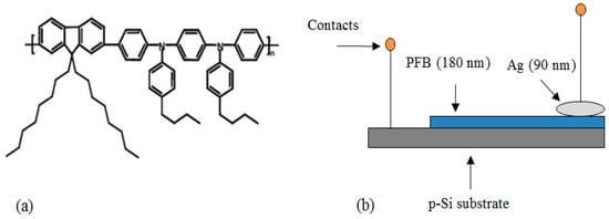
Figure 1.
(a) Molecular structure of PFB and (b) schematic diagram of Ag/PFB/p-Si heterojunction.
3. Results
To probe surface morphology of PFB thin film, deposited on p-Si substrate, SEM and AFM analyses were performed. Figure 2a shows SEM images of PFB thin film. The micrograph reveals the porous sponge-like structure of the film, which improves the sensing mechanism of the film. This type of structure makes it suitable for deposition over flexible substrate. Moreover, such films can be employed in a number of applications such as photodetectors, solar cells, and sensors. The micrograph also exhibits some agglomeration that produces discontinuity in the film and affects the flow of current. The agglomerates and discontinuity in the film are believed to be responsible for lowering the current in the diode and thus the mobility. Further investigations on the morphology of the film can be carried out to improve the conductivity of the film. Energy dispersive X-ray spectroscopy (EDX) is a very important technique employed for elemental analysis of the sample. Figure 2b shows the EDX spectrum of the PFB polymer thin film. The peaks in the spectrum provide information about the elements and their percentage existence. The higher peak intensity in the spectrum shows higher concentration of Si. It is confirmed from the spectra that the PFB thin film/p-Si comprises carbon (C), oxygen, and Si. As from the molecular structure of PFB—shown in Figure 1a—it does not contain Si and oxygen; however, these elements appear in the EDX spectrum with highest intensities. The source of Si and oxygen peaks in the spectrum is the Si substrate and the possible oxide layer on Si, respectively. It is due the fact that the EDX beam has large penetration depth and is able to go through the PFB thin film to reach the Si substrate. Whereas, the peak of C arises from the PFB film. Since the SEM micrograph reveals some roughness, the AFM analysis is performed in a noncontact mode to estimate the film roughness of PFB thin film. The 2D and 3D AFM images of PFB polymer on p-Si substrate are shown in Figure 2c,d, respectively. The micrographs exhibit rough and nonuniform film. Moreover, the 3D image shows fairly high spikes. From the AFM analysis, root-mean square (RMS) roughness of the PFB film was found to be 25 ± 10 nm, which is 13.9% of the total film thickness (180 nm). The grains are randomly oriented with distinct sizes and shapes, which is in agreement with the SEM analysis. The nonuniform surface profile due to random distribution and size of grains produce discontinuity in the film that act as potential wells and are responsible for limiting the current by trapping charge carriers.
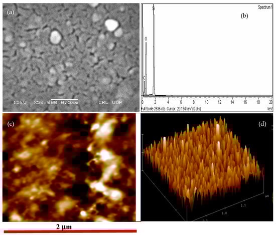
Figure 2.
Surface morphology of PFB thin film: (a) SEM micrograph, (b) EDX spectrum, (c) 2D atomic force microscope (AFM) micrograph, and (d) 3D AFM image of PFB thin film.
The absorption spectrum of PFB polymer on p-Si substrate is shown in Figure 3a. There are two distinct sharp peaks in the spectrum, which correspond to the Soret band and the Q-band. The first peak appearing at 220 nm lies in the ultraviolet spectral region (Soret band) and the second peak lies at 380 nm and its shoulder at 320 nm lies in the visible region (Q-band). There is a complete agreement of the acquired results with the those reported previously [25]. The optical bandgap is calculated from the plot of (αE)2 versus E, shown in Figure 3b, by extrapolating the linear part of (aE)2 to zero. Here, E denotes the energy of absorbed light and α is the absorption coefficient. The optical bandgaps were estimated for visible region and infrared regions as 2.88 and 5.22 eV, respectively. The X-ray diffraction pattern of PFB film, at room temperature, is shown in Figure 3c. It can be clearly seen from the figure that there is no significant peak in the curve, which verifies the noncrystalline nature of PFB. Instead a characteristic hump at 2θ ≈ 20° and noisy behavior in the XRD diffractogram is observed, which imply π–π stacking of the aromatic rings in PFB polymer and exhibits the amorphous nature of PFB.
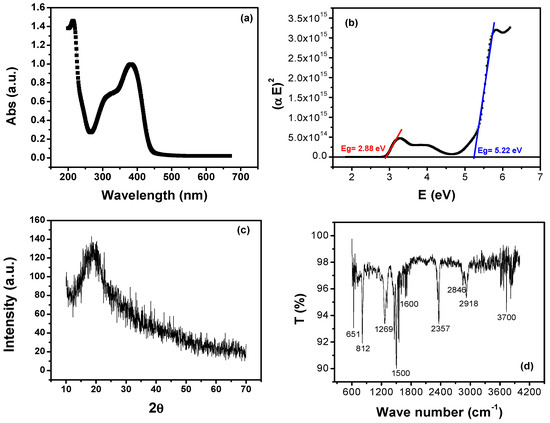
Figure 3.
(a) UV–vis absorption spectrum, (b) Tauc’s plot for bandgap measurement, (c) XRD diffractogram, and (d) FTIR spectrum of PFB thin film.
The bond dynamics of PFB are investigated by FTIR spectroscopy within a wide energy range of 600–4200 cm−1, as shown in Figure 3d. In the FTIR spectroscopy, one measures the absorption/transmission of photons by molecules in the infrared (IR) region. Furthermore, different peaks represent the areas of IR spectrum where specific bond vibrations occur. The FTIR spectrum acts as a fingerprint for the identification of different compounds, molecules, functional groups, and nature of their bonds. From left to right, two strong peaks are observed at 651 and 812 cm−1, both of which correspond to C-H bending vibration. A medium-strong peak at 1269 cm−1 reveals C-N stretching, whereas an intense peak at 1500 cm−1 demonstrates C-C stretching mode. The medium-weak peak at 1600 cm−1 and strong spike at 2357 cm−1 are attributed to C=C stretching of conjugated alkene and C≡C stretching modes, respectively. There are also some relatively broad and weak peaks at 2846–2918 cm−1 containing C-H stretch mode. The sample displays a relatively broad intense hydrogen-bonded O-H stretch absorption centered on 3700 cm−1. The overall FTIR analysis of PFB is presented in Table 1.

Table 1.
PFB molecular composition with chemical bond dynamics.
To study the microelectronic properties of the Ag/PFB/p-Si heterojunction, I–V characteristics are carried out at 300 K in dark conditions. The I–V graph shown in Figure 4a is nonlinear and asymmetric, which demonstrate that p-Si/PFB heterojunction exhibits rectifying current behavior in the forward bias. An exponential increase in the forward current is observed due to the formation of a depletion region between the p-Si and PFB thin film. Rectification ratio (RR), the ratio of forward and reverse current, is extracted from the I–V curve of the heterojunction whose maximum value is found to be 23.6 at ±7.2 V, and the value of turn-on voltage Vturn on is 3.92 V. In the case of heavily doped semiconductors, rectifying behavior of the heterojunction is well described by thermionic emission–diffusion theory and/or field emission theory [26]. Assuming that PFB has as much high hole mobility as a heavily doped p-type semiconductor [27], then the forward-bias characteristics of the Ag/PFB/p-Si can be studied by thermionic emission–diffusion theory according to Equation (1). The current can be calculated by the following equation:
where I is forward current, I0 represents reverse saturation current, n is the ideality factor, q is electronic charge, V is applied voltage, Rs is series resistance, T is absolute temperature, and k is the Boltzmann constant. I0 in Equation (1) can be expressed as:
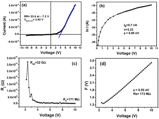
Figure 4.
(a) I–V curves at room temperature, (b) ln (I)–V characteristics, (c) junction resistance vs. V curve, and (d) F(V) vs. V plot for the Ag/PFB/p-Si device.
In Equation (2), A is the area of the diode, A* is the effective Richardson constant (32 A/cm2 k2 for p-Si [28]), and Φb is barrier height. The following equation is used to calculate n:
At V around 0 V, I0 is obtained from the intercept of the semilogarithmic I–V characteristics of the plot shown in Figure 4b. The value of I0 calculated from the ln(I)–V curve is 0.07 nA, whereas the value of Φb is extracted from the y-intercept of the ln(I)–V characteristics in the forward region. It is calculated from the following equation:
Using Equation (4), Φb is found to be 0.89 eV, which is a key parameter to determine the behavior of the depletion region in the heterojunction device. In p-type semiconductors such as PFB, Φb manifests itself as the energy difference between the Fermi level and the maximum valence band that controls the flow of holes across the interface of the device [29].
The ln(I)–V characteristics are used to find the value of n for the Ag/PFB/p-Si heterojunction. The n normally describes dependence of the diode current on applied voltage and compares the quality of the fabricated device with that of the ideal one. For an ideal rectifying device (diode) the value of n is “one”; however, in practice, n always exceed unity [30] due to the possible formation of oxide layer on Si surface, which acts as insulating layer and results in increasing Rs at the interface of PFB/p-Si [31]. From the ln(I)–V curve, along with Equation (3), n is calculated to be 3.23. Recently, it was widely reported that the value of n varies from 2 to 11 for organic-semiconductor-based rectifying devices [32,33,34,35,36]. In the present case, the higher value of n = 3.23 can be ascribed to Rs and the nonuniform surface profile of PFB thin film, which can be observed from the SEM and AFM images. Still, this value is small and closer to one when compared to the reported values for n in the case of other organic semiconductors. Hence, PFB/p-Si heterojunction can find its potential applications in electronic and optoelectronic devices.
Besides the significance of Rs, the performance and stability of the device also depend on shunt resistance (Rsh). Ideally, zero value of Rs allows maximum flow of charge in the device, while significantly high (infinite) values of Rsh cause minimum leakage current. A graph is plotted between the junction resistance Rj = dV/dI vs. V, as shown in Figure 4c, to calculate the values of Rsh and Rs for the Ag/PFB/p-Si heterojunction device. The flat portion of I–V characteristics provides the value of Rs, while Rsh is obtained from the highest peak value in the graph. The extracted values of Rsh and Rs from the graph are 32 GΩ and 171 MΩ, respectively. The deviation of the Ag/PFB/p-Si device from ideal behavior is due to the Rs = 171 MΩ across the heterojunction of PFB/p-Si.
Norde’s function is an alternate technique to determine and/or cross-verify the values obtained for Φb and Rs [37]. Norde’s function is expressed by Equation (5):
The F(V0) denotes minimum value of F(V), I0 represents current at V = V0, and shows an integer whose value is always greater than “n”. The F(V) vs. V plot is shown in Figure 4d for the Ag/PFB/p-Si device. Using Equations (5)–(7) along with Figure 4d, the values of Rs and Φb are extracted to be 173 MΩ and 0.93 eV, respectively. This method renders concordant results with the conventional I–V method, as shown in Table 2.
Table 2.
Comparison of various parameters of the Ag/PFB/p-Si device extracted from the conventional I-V and Norde’s techniques.
The high value of n obtained for the Ag/PFB/p-Si device is possibly due to the presence of interfacial states at the heterojunction, which further implies that the thermionic emission is not the only dominating charge carrier transport mechanism [38]; however, there exist some other conduction mechanisms as well. The charge transport mechanisms in the Ag/PFB/p-Si device are studied from double logarithmic I–V (log I vs. log V) characteristics according to power/Child’s law, i.e., I ∝ Vm, where m is the slope of a linear portion of the log I vs. log V curve, as shown in Figure 5. As reported elsewhere [39,40], there are various regions in the graph that can be explained on the basis of the power law of current. The region, for which m = 1, is an ohmic region, m = 2 yields the space-charge limited current (SCLC) region and m > 2 demonstrates the trapped-charge limited current (TCLC) region [41]. It can be observed from Figure 5 that the Ag/PFB/p-Si device has three distinct regions. At low voltages, region 1 (0.38 < log V < 0.44) has a slope m equal to 3.8. This region conforms to the TCLC mode of conduction. The carriers injected at the interface cause current to flow in proportion to the square of applied bias, obeying Child’s law. In this region, the density of injected free charge-carriers is much greater than that of the thermally generated free charge-carrier [42]. Subsequently, in the intermediate voltage range of region 2 (0.45 < log V < 0.66), m = 1. This region is governed by an ohmic transport mechanism, where current increases linearly with the applied voltage because effective density of injected carriers might be less than the thermal carrier density [43]. In region 3, at higher voltages (0.67 < log V < 1), the slope almost equals 0.5, indicating that the dominant conduction mechanism in this domain is thermionic emission, where free carriers are thermally generated at the interface of the top electrode, Ag, and organic layer PFB.
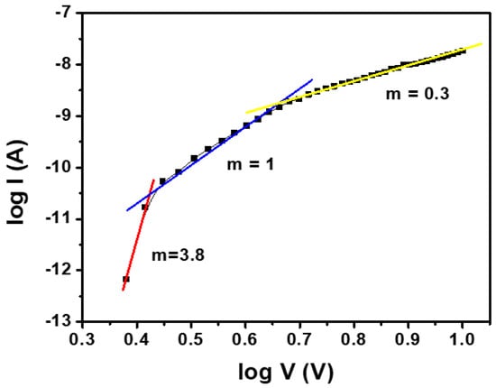
Figure 5.
The forward log I vs. log V graph of the Ag/PFB/p-Si device.
Overall comparison of the microelectronic parameters of Ag/PFB/p-Si heterojunction and those of other organic semiconductor/p-Si devices reported elsewhere [25] are given in Table 3. The comparison reveals that the Ag/PFB/p-Si device can overtake the existing similar devices in several key microelectronic parameters. However, higher value of Rs might be the reason for the divergence of the diode from the ideal behavior.
Table 3.
Comparison of device parameters of the Ag/PFB/p-Si heterojunction with the previously reported heterojunction devices.
4. Conclusions
The Ag/PFB/p-Si heterojunction is fabricated by using PFB as an active semiconducting layer with Ag as ohmic contact. The microelectronic properties of the Ag/PFB/p-Si device are studied by two different characterization methods, i.e., conventional I–V and Norde’s functions. It is observed that the measured device parameters (smaller value of n and I0) confirms better quality of the PFB/p-Si heterojunction. The lower ratio of Rs to Rsh demonstrates relatively stable junction of PFB/p-Si. The microelectronic parameters obtained from Norde’s functions are in closer agreement with those obtained from the conventional I–V method. From the SEM and AFM analysis, the surface features of PFB film are nonuniform, which results in a higher value of Rs that subsequently decreases the current across the PFB/p-Si interface. XRD reveals the amorphous nature of PFB, whereas UV–vis spectrum exhibits its optical bandgap as 2.88 eV in the visible range. On the basis of this study, PFB is proposed to be used as an active material for its potential applications in electronics and optoelectronics.
Author Contributions
Conceptualization, M.T. and M.I.; methodology, M.I., M.T., and M.Z.; software, M.I. and M.T.; validation F.A., M.R.S., and M.T.; formal analysis, M.T. and M.R.S.; investigation, M.T. and M.Z.; resources, M.I. and M.T.; data curation, M.Z. and M.R.S.; writing—M.I. and M.T.; writing—review and editing, M.T.; M.I., F.A., and M.R.S.; supervision, M.T.; project administration, M.T.; funding acquisition, M.A.I. and R.M. All authors have read and agreed to the published version of the manuscript.
Funding
Universiti Kebangsaan Malaysia (UKM) for funding the research under Grant Code GUP-2017-093.
Acknowledgments
All the authors are grateful to the Abdul Wali Khan University Mardan, Pakistan, Higher Education Commission (HEC) of Pakistan, for providing the research facilities and Project No. 10170/KPK/NRPU/R&D/HEC.
Conflicts of Interest
The authors declare no conflict of interest.
References
- Islam, Z.U.; Tahir, M.; Syed, W.A.; Aziz, F.; Wahab, F.; Said, S.M.; R Sarker, M.; Md Ali, S.H.; Sabri, M.F.M. Fabrication and Photovoltaic Properties of Organic Solar Cell Based on Zinc Phthalocyanine. Energies 2020, 13, 962. [Google Scholar] [CrossRef]
- Chen, Z.; Obaid, S.N.; Lu, L. Recent advances in organic optoelectronic devices for biomedical applications. Opt. Mater. Express 2019, 9, 3843. [Google Scholar] [CrossRef]
- Kim, J.T.; Lee, J.; Jang, S.; Yu, Z.; Park, J.H.; Jung, E.D.; Lee, S.; Song, M.H.; Whang, D.R.; Wu, S.; et al. Solution processable small molecules as efficient electron transport layers in organic optoelectronic devices. J. Mater. Chem. A 2020, 8, 13501–13508. [Google Scholar] [CrossRef]
- Zeb, M.; Tahir, M.; Muhammad, F.; Mohd Said, S.; Mohd Sabri, M.F.; R Sarker, M.; Hamid Md Ali, S.; Wahab, F. Amplified Spontaneous Emission and Optical Gain in Organic Single Crystal Quinquethiophene. Crystals 2019, 9, 609. [Google Scholar] [CrossRef]
- Preliminary Study of Effective Copper Indium Sulfide (CuInS2) Quantum Dots as Photo-Sensitizer in Solar cell-UKM Journal Article Repository. Available online: http://journalarticle.ukm.my/15337/ (accessed on 16 October 2020).
- Jiang, Y.; Liu, Y.-Y.; Liu, X.; Lin, H.; Gao, K.; Lai, W.-Y.; Huang, W. Organic solid-state lasers: A materials view and future development. Chem. Soc. Rev. 2020, 49, 5885–5944. [Google Scholar] [CrossRef]
- Kleemann, H.; Krechan, K.; Fischer, A.; Leo, K. A Review of Vertical Organic Transistors. Adv. Funct. Mater. 2020, 30, 1907113. [Google Scholar] [CrossRef]
- Tahir, M.; Muddusir; Khan, D.N.; Gul, S.; Wahab, F.; Said, S.M. Photovoltaic effect on the microelectronic properties of perylene/p-Si heterojunction devices. J. Mater. Sci. Mater. Electron. 2019, 30, 19463–19470. [Google Scholar] [CrossRef]
- Sinin, N.A.M.; Ibrahim, M.A.; Sepeai, S.; Sulaiman, M.Y.; Teridi, M.A.M.; Ludin, N.A.; Zaidi, S.H. Modification of BSF layer in bifacial solar cell via photosensitization of molecules nanostructure. J. Teknol. 2016, 78, 109–114. [Google Scholar]
- Zeb, M.; Tahir, M.; Muhammad, F.; Khan, D.N.; Sayyad, M.H.; Said, S.M.; Wahab, F. Perylene Tetracarboxylic Diimide: Characterization and Its Role in the Electrical Properties of an Ag/N-BuHHPDI/PEDOT:PSS/p-Si Heterojunction Device. J. Electron. Mater. 2019, 49, 395–401. [Google Scholar] [CrossRef]
- Muhammad, F.; Tahir, M.; Zeb, M.; Uddin, S.I.; Ahmed, S. Enhancement in the Microelectronic Properties of a PFB–CdSe Quantum Dots Nanocomposite Based Schottky Barrier Diode. J. Electron. Mater. 2019, 48, 5169–5175. [Google Scholar] [CrossRef]
- Fatima, N.; Karimov, K.S.; Qasuria, T.A.; Ibrahim, M.A. A novel and stable way for energy harvesting from Bi2Te3Se alloy based semitransparent photo-thermoelectric module. J. Alloy. Compd. 2020, 849, 156702. [Google Scholar] [CrossRef] [PubMed]
- Roenker, K.P.; Cahay, M. Simulation of Pentacene Organic Metal-Oxide Field Effect. Ph.D. Thesis, University of Cincinnati, Cincinnati, OH, USA, 2003. [Google Scholar]
- McNeill, C.R.; Greenham, N.C. Conjugated-polymer blends for optoelectronics. Adv. Mater. 2009, 21, 3840–3850. [Google Scholar] [CrossRef]
- Muhammad, F.; Tahir, M.; Zeb, M.; Kalasad, M.N.; Mohd Said, S.; Sarker, M.R.; Sabri, M.F.M.; Ali, S.H.M. Synergistic enhancement in the microelectronic properties of poly-(dioctylfluorene) based Schottky devices by CdSe quantum dots. Sci. Rep. 2020, 10, 1–13. [Google Scholar] [CrossRef] [PubMed]
- McNeill, C.R.; Watts, B.; Swaraj, S.; Ade, H.; Thomsen, L.; Belcher, W.; Dastoor, P.C. Evolution of the nanomorphology of photovoltaic polyfluorene blends: Sub-100 nm resolution with x-ray spectromicroscopy. Nanotechnology 2008, 19, 424015. [Google Scholar] [CrossRef]
- Al-Hardan, N.H.; Jalar, A.; Abdul Hamid, M.A.; Keng, L.K.; Ahmed, N.M.; Shamsudin, R. A wide-band UV photodiode based on n-ZnO/p-Si heterojunctions. Sens. Actuators A Phys. 2014, 207, 61–66. [Google Scholar] [CrossRef]
- Kressel, H. Materials for Heterojunction Devices. Annu. Rev. Mater. Sci. 1980, 10, 287–309. [Google Scholar] [CrossRef]
- Mustakim, N.S.M.; Sepeai, S.; Ludin, N.A.; Teridi, M.A.M.; Ibrahim, M.A. Properties of nanostructured rutile titanium dioxide (TiO2) thin film deposited with silver sulfide (Ag2S) quantum dots as photoanode for solar photovoltaic. In Solid State Phenomena; Trans Tech Publications Ltd.: Stafa-Zurich, Switzerland, 2019; Volume 290, pp. 329–335. [Google Scholar]
- Mohamed Mustakim, N.S.; Ubani, C.A.; Sepeai, S.; Ahmad Ludin, N.; Mat Teridi, M.A.; Ibrahim, M.A. Quantum dots processed by SILAR for solar cell applications. Sol. Energy 2018, 163, 256–270. [Google Scholar] [CrossRef]
- Rost, C.; Gundlach, D.J.; Karg, S.; Rieß, W. Ambipolar organic field-effect transistor based on an organic heterostructure. J. Appl. Phys. 2004, 95, 5782–5787. [Google Scholar] [CrossRef]
- Forrest, S.R.; Kaplan, M.L.; Schmidt, P.H. Organic-on-inorganic semiconductor contact barrier diodes. II. Dependence on organic film and metal contact properties. J. Appl. Phys. 1984, 56, 543–551. [Google Scholar] [CrossRef]
- Wang, H.; Wang, J.; Huang, H.; Yan, X.; Yan, D. Organic heterojunction with reverse rectifying characteristics and its application in field-effect transistors. Org. Electron. 2006, 7, 369–374. [Google Scholar] [CrossRef]
- Xu, Y.; Berger, P.R.; Cho, J.; Timmons, R.B. Capacitance-voltage characterization of pulsed plasma polymerized allylamine dielectrics for flexible polymeric field effect transistors. J. Electron. Mater. 2004, 33, 1240–1247. [Google Scholar] [CrossRef]
- Seoudi, R.; El-Bahy, G.S.; El Sayed, Z.A. Ultraviolet and visible spectroscopic studies of phthalocyanine and its complexes thin films. Opt. Mater. 2006, 29, 304–312. [Google Scholar] [CrossRef]
- Physics of Semiconductor Devices, 2nd ed.; John Wiley and Sons: New York, NY, USA, 18 November 1981.
- Singh, A.K.; Prakash, R.; Dwivedi, A.D.D.; Chakrabarti, P. Electronic properties and junction behavior of polyanthranilic acid/metal contacts. IEEE Electron Device Lett. 2008, 29, 571–574. [Google Scholar] [CrossRef]
- Tahir, M.; Sayyad, M.H.; Wahab, F.; Khan, D.N. The electrical characterization of Ag/N-BuHHPDI/p-Si heterojunction by current-voltage characteristics. Mod. Phys. Lett. B 2013, 27, 1350080. [Google Scholar] [CrossRef]
- Tung, R.T. The physics and chemistry of the Schottky barrier height. Appl. Phys. Rev. 2014, 1, 011304. [Google Scholar]
- Sze, S.M.; Ng, K.K. Physics of Semiconductor Devices; John Wiley & Sons, Inc.: Hoboken, NJ, USA, 2006; ISBN 9780470068328. [Google Scholar]
- Akkiliç, K.; Uzun, I.; Kiliçoǧlu, T. The calculation of electronic properties of an Ag/chitosan/n-Si Schottky barrier diode. Synth. Met. 2007, 157, 297–302. [Google Scholar] [CrossRef]
- Grant, P.M.; Tani, T.; Gill, W.D.; Krounbi, M.; Clarke, T.C. Properties of metal/polyacetylene Schottky barriers. J. Appl. Phys. 1981, 52, 869–872. [Google Scholar] [CrossRef]
- Turut, A.; Köleli, F. Semiconductive polymer-based Schottky diode. J. Appl. Phys. 1992, 72, 818–819. [Google Scholar] [CrossRef]
- Nazarova, I.B.; Krinichnyi, V.I.; Goldenberg, L.M. Schottky diodes based on poly(p-phenylene) and poly(1,4-dipyrrolobenzene). Synth. Met. 1993, 53, 399–402. [Google Scholar] [CrossRef]
- Gamier, F.; Horowitz, G. Organic Semiconducting Polymers for New Electronic Devices; Springer: Berlin/Heidelberg, Germany, 1987; pp. 423–427. [Google Scholar]
- Chen, S.A.; Fang, Y.; Lee, H.T. Polyacrylic acid-doped polyaniline as p-type semiconductor in Schottky barrier electronic device. Synth. Met. 1993, 57, 4082–4086. [Google Scholar] [CrossRef]
- Norde, H. A modified forward I-V plot for Schottky diodes with high series resistance. J. Appl. Phys. 1979, 50, 5052–5053. [Google Scholar] [CrossRef]
- Taguchi, R.; Kobayashi, T.; Muto, J. Characteristics of electrochromic magnesium phthalocyanine films for initial oxidation-reduction cycling. J. Mater. Sci. Lett. 1994, 13, 1320–1322. [Google Scholar] [CrossRef]
- Carbone, A.; Kotowska, B.K.; Kotowski, D. Space-charge-limited current fluctuations in organic semiconductors. Phys. Rev. Lett. 2005, 95, 236601. [Google Scholar] [CrossRef] [PubMed]
- Lee, J.; Hwang, D.K.; Park, C.H.; Kim, S.S.; Im, S. Pentacene-based photodiode with Schottky junction. In Proceedings of the Thin Solid Films; Elsevier: Amsterdam, The Netherlands, 2004; Volume 451–452, pp. 12–15. [Google Scholar]
- Aydin, M.E.; Türüt, A. The electrical characteristics of Sn/methyl-red/p-type Si/Al contacts. Microelectron. Eng. 2007, 84, 2875–2882. [Google Scholar] [CrossRef]
- Güllü, Ö.; Aydoǧan, Ş.; Türüt, A. Fabrication and electrical characteristics of Schottky diode based on organic material. Microelectron. Eng. 2008, 85, 1647–1651. [Google Scholar] [CrossRef]
- Aydoǧan, Ş.; Incekara, Ü.; Deniz, A.R.; Türüt, A. Extraction of electronic parameters of Schottky diode based on an organic Orcein. Microelectron. Eng. 2010, 87, 2525–2530. [Google Scholar] [CrossRef]
- Tahir, M.; Sayyad, M.H.; Wahab, F.; Aziz, F.; Shahid, M.; Munawar, M.A. Perylene diimide: Synthesis, fabrication and temperature dependent electrical characterization of heterojunction with p-silicon. Phys. B Condens. Matter 2013, 426, 6–12. [Google Scholar] [CrossRef]
- Poddar, R.; Luo, C. A novel approach to fabricate a PPy/p-type Si heterojunction. Solid State Electron. 2006, 50, 1687–1691. [Google Scholar] [CrossRef]
Publisher’s Note: MDPI stays neutral with regard to jurisdictional claims in published maps and institutional affiliations. |
© 2020 by the authors. Licensee MDPI, Basel, Switzerland. This article is an open access article distributed under the terms and conditions of the Creative Commons Attribution (CC BY) license (http://creativecommons.org/licenses/by/4.0/).