Article

Amplification of Radiation-Induced Signal of LED Strip by Increasing Number of LED Chips and Using Amplifier Board

by
Edrine Damulira
1,*,
Muhammad Nur Salihin Yusoff
1,*,
Ahmad Fairuz Omar
2 and
Nur Hartini Mohd Taib
3
1
Medical Radiation Programme, School of Health Sciences, Universiti Sains Malaysia, Kubang Kerian 16150, Malaysia
2
Engineering Physics Laboratory, School of Physics, Universiti Sains Malaysia, Penang 11800, Malaysia
3
Department of Radiology, School of Medical Sciences, Universiti Sains Malaysia, Kubang Kerian 16150, Malaysia
*
Authors to whom correspondence should be addressed.
Appl. Sci. 2020, 10(2), 651; https://doi.org/10.3390/app10020651
Submission received: 6 December 2019 / Revised: 8 January 2020 / Accepted: 11 January 2020 / Published: 16 January 2020
(This article belongs to the Special Issue GaN-Based Light-Emitting Diodes)

Abstract

:

Featured Application

This work could initiate a cutting-edge technology that exploits dual applicability of LEDs i.e., not only for the classical purpose as a luminary, but also for medical radiation detection (diagnostic X-rays).

Abstract

Transducers, such as photodiodes, phototransistors, and photovoltaic cells are promising radiation detectors. However, for accurate radiation detection and dosimetry, signals that emanate from these devices have to be sufficient to facilitate accurate calibrations, i.e., assigning a quantity of radiation dose to a specific magnitude of the signal. More so, purposely fabricated for luminescence, LEDs produce significantly low signals during radiation detection applications. Therefore, this paper investigates the enhancement and augmentation of photovoltaic signals that were generated when LED strips were being exposed to diagnostic X-rays. Initially, signal amplification was achieved through increasing the effective LED active area (from 60 to 120 chips); by successively connecting LED strips. Further, signal amplification was undertaken by injecting the raw LED strip signal into an amplifier board with adjustable gains. In both the signal amplification techniques, the tube voltage (kVp), tube current-time product (mAs), and source-to-detector distance (SDD) were varied. The principal findings show that effective active area-based signal amplifications produced an overall average of 91.16% signal enhancement throughout all of the X-ray parameter variations. On the other hand, the amplifier board produced an average of 36.48% signal enhancement for the signals that were injected into it. Chip number increment-based signal amplifications had a 0.687% less coefficient of variation than amplifier board signal amplifications. The amplifier board signal amplifications were impaired by factors, such as dark currents, amplifier board maximum operational output voltage, and saturation. Therefore, future electronic signal amplification could use amplifier boards having low dark currents and high operational voltage headroom. The low-cost and simplicity that are associated with active-area amplification could be further exploited in a hybrid amplification technique with electronic amplification and scintillators.

1. Introduction

Silicon, being the most abundant element on earth [1], has facilitated the large-scale production of innumerable silicon-based electronic circuit components such as photonic devices. Therefore, photonic devices are readily available at low cost and are fundamentally fabricated for luminescence applications—detect and produce light. However, medical applications not only use photonic devices for luminescence, but also for diagnostic and therapeutic radiation detection [2].
Multiplication registers and intensifier screens implement sensitivity enhancement in charge-coupled devices (CCDs), such as electron-multiplying CCDs (EMCCDs) and intensified CCDs (ICCDs), respectively [3]. Consequently, EMCCDs and ICCDs have a notably higher sensitivity than traditional CCDs—especially while detecting extremely low light photons [3].
Semiconductor-based detectors, such as avalanche photodiodes (APDs), are also associated with intrinsic signal amplification [4]. However, transimpedance amplifiers and bipolar junction transistors are applied to externally amplify photodiode detected signals [5,6,7]. Therefore, photonic device raw signal amplification is of paramount importance—particularly for low radiation-induced signal detection [8,9,10].
The current literature and research results have established LEDs as visible light/optical [11,12,13] and diagnostic X-ray [14] detectors. In applications [11,12,13], two LEDs were employed (one LED as a light emitter and the other as a detector of the light emitted by the first LED) in the form of a paired emitter detector diode (PEDD). Besides, the comparison of blue and red LED emission and sensitivity spectra discovered drift of the LED detection sensitivity to shorter wavelengths—for both the tested LEDs [11]. This LED sensitivity to short wavelengths could imply the ability to detect electromagnetic radiation with short wavelengths, e.g., diagnostic X-rays. LEDs could, thus, be an alternative detection device for diagnostic X-rays, because they are not only spectrally selective (detect a specific wavelength range) [11,15], but could also be resistant to diagnostic X-ray-induced structural damages [16,17] (in comparison to other photodetectors, such as photodiodes). The output signal achieved during detection-mode is very low because LEDs are optimized for luminescence (~0.5–4.5 nA [11]).
LED luminary output enhancements, such as those that were observed in [18], have been executed. These have greatly improved the efficiency of LEDs as light emitters. Contrastingly, similar studies augmenting LED efficiency as a detector are non-existent in the present-day literature.
Although research [11] has highlighted that LED visible-light-induced signals could be approximately ten times as low as that of photodiode visible-light-induced signals, there is still little evidence regarding the technique to enhance the sensitivity of LEDs—when employed as detectors for diagnostic X-rays. More so, in the early nineties, the application of LEDs as detectors was mainly discouraged due to low detected signals; the technology then was not adequate for providing a solution to this setback [11]. In our earlier work [14], the cold white LED strip was characterized with the best dosimetric response in comparison to warm white, red, green, and blue LED strips. This work approved our further exploitation of the cold white LED strip for dosimetry applications with respect to dosimetric traits, such as LED signal linearity to diagnostic X-ray dose and tube current-time product (mAs), and slight degradations in LED signal output as a consequence of accumulated dose/increased radiation exposure. Even though quantifiable, the cold white signals were low and they ranged from 0 to 1.1 mV.
Today, operational amplifiers and high gain transistors are applied to amplify the electrical output signals of photodiodes [5]. This study similarly utilizes an amplifier board as a sensitivity augmentation method, because both photodiodes and LEDs mainly consist of PN junctions; the board mainly comprises operational amplifiers and transistors. This methodology concurs with that of Bui’s group [11] that amplified a PEDD’s photovoltaic signal while using an operational amplifier. In the other sensitivity enhancement approach, the LED sensitive/active area was increased by increasing the number of LED chips. In both sensitivity augmentation methods, our LEDs were in the photovoltaic configuration—similar to elsewhere [12,13]. Stated otherwise, we did not apply any biasing voltage to the LEDs. Applying a negative voltage to the LEDs (photoconductive configuration) would lead to the detection of dark currents, which would make it difficult to distinguish the low diagnostic radiation-induced signal from the dark current.
Therefore, this study aims at enhancing the sensitivity of LEDs to diagnostic X-rays by amplifying its radiation-induced current.

2. Materials and Methods

2.1. Experimental Set-Up

X-ray beams from a static X-ray tube (Quantum Medical Imaging, New York, NY, USA) were perpendicularly incident on 12 V DC SMD 5050 cold white LED strips. These cold white LED strips constitute a gallium-nitride (GaN) semiconductor that was coated with a phosphor. Each strip had 12 chips, and the sensitive area for each chip was approximately 12.6 mm2. During the LED strip fabrication, these chips were connected in parallel by the manufacturer.
The X-ray tube was operated in a non-automatic exposure control (AEC) mode, and the field size was collimated to 26 × 26 cm2 for all of the exposures in this study. The tube voltage was manually adjusted in steps of 10 from 70 to 140 kVp, while maintaining a constant tube current-time product and source-to-detector distance (SDD) of 80 mAs and 60 cm, respectively. However, the tube current-time product setting had pre-set values of 20.2, 25.6, 32, 40, 51.2, 64, 80, 102.4, 128, 160, 201.6, and 256 mAs and the tube voltage and SDD were kept constant at 120 kVp and 80 cm, respectively. While fixing the tube voltage and current-time product at 120 kVp and 256 mAs respectively, the SDD was varied from 60 to 90 cm—in 5 cm steps. A 30 cm × 30 cm × 8 cm solid water phantom slab absorbed the treatment couch sourced backscattered radiation, as observed in Figure 1.
Ambient light signals were mitigated by executing the irradiations in a light-tight surrounding and then masking the LED chip sensitive areas with black vinyl tape. Despite these mitigations, an ambient signal (0–0.2 mV)—perhaps due to ambient temperature/heat, was observed before irradiations; whilst directly injecting the signal into the multimeter. The ambient signal was deducted from the total detected signal to obtain the net radiation-induced signal.
A single-channel dosimeter probe (A-CF1E1003, Iba Dosimax plus: Schwarzenbruck, Germany) was simultaneously irradiated with the LED chips. The dosimeter’s measurable parameter ranges were absorbed dose; 200 nGy–9999 mGy, dose rate; 80 nGy/s–70 mGy/s for 50–150 kV; and time (1 ms–19,999 s).
An electric cable wire for LED strip lighting (Red and Black Tinned Copper 22 AWG wire, Lustreon) was deployed for inter-strip connections. The cable also transmitted the raw photovoltaic signal (radiation-induced current) to a digital multimeter/oscilloscope (Model JDS2012A, Jinhan Company: Hefei, Anhui, China). The signal reading was displayed in the form of voltage—mV.

2.2. Signal Enhancement

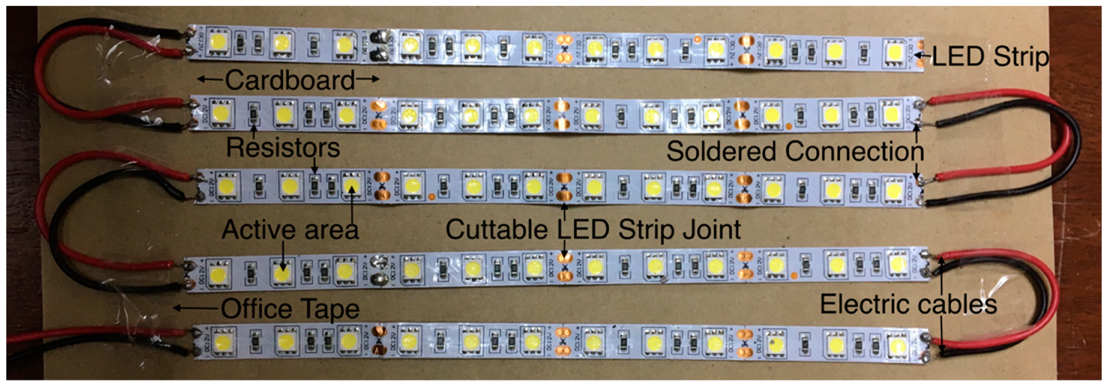
2.2.1. LED Chip Number/Active Area Increment

Preliminary Exposure to Visible Light

The LED chip number was increased in multiples of 12 during the investigation of the effect of active area increment on the LED strip detectability of visible light; each strip had 12 LED chips, as observed in Figure 2. In other words, the active area was increased from 151.2 mm2 (12.6 mm2 × 12) to 907.2 mm2 (12.6 mm2 × 72)—in steps of 151.2 mm2. The LED strip was cut (to fit the field size) and reconnected by soldering while using a soldering wire (SW600622 DIA) with a diameter of 0.8 mm.

Exposure to Diagnostic X-rays

To limit X-ray radiation exposure, only two exposure sets were executed in the examination of LED strip sensitivity enhancement by increasing the sensitive area. In the first exposure set, the kVp, mAs, and SDD parameter adjustments in Section 2.1 were executed with a total of 60 LED chips (active area of 756 mm2). For the second exposure set, the LED chip number was doubled to 120 LED chips (active area of 1512 mm2), while maintaining the same exposure settings in the first exposure set.

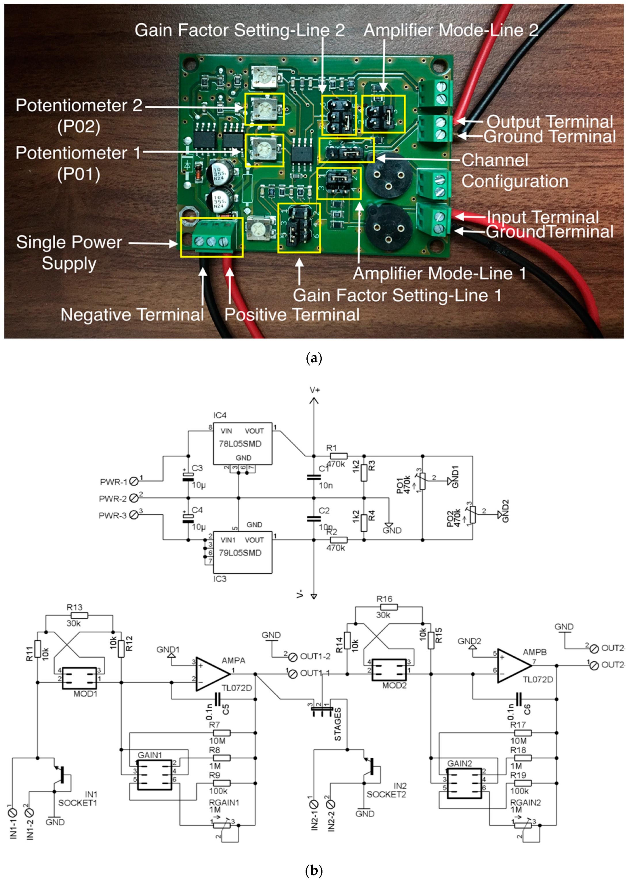
2.2.2. Amplifier Board

In Section 2.2.1, the LED strip signal was directly injected into the multimeter. However, in this sub-section, the signal was first fed into a multifunctional amplifier board (TW-MF2CAB Sglux: Berlin, Germany); this amplifier board is mostly applied in blind Ultraviolet (UV)-detector photocurrent amplifications. This amplifier board is commercially available in electronics online stores. The board’s dimensions are 60 mm × 45 mm × 12 mm and it was powered with a single power supply of 26 V—Figure 3. As elaborated in Figure 3b, this board is composed of circuit components, which include resistors, transistors, capacitors, potentiometers, and operational amplifiers. Before injecting any signal into the amplifier board, the potentiometers 1 and 2 were adjusted to ensure that the board’s dark current is below 1 mV, as recommended by the manufacturer. The post-amplifier board signal was then transported through the electric cable and injected into the digital multimeter.
The amplifier board was set to a two-channel sequential amplification configuration. In the first amplification stage, the amplifier mode-line 1 was set to a transimpedance amplifier, and its gain factor setting-line 1 was 107 V/A. In the second amplification stage, the amplifier mode-line 2 was set to a voltage amplifier with a pre-gain of 10 V/V. The gain factor setting line 2 was also adjusted to a voltage gain of 10 V/V. Therefore, the second amplification stage had a total voltage gain of 100 V/V. This amplification combination produced a dark current of 0.8 mV, which was below the operational dark current of 1 mV, as recommended by the amplifier board manufacturer.
However, the dark current increased to 1.3 mV when the second amplification stage setting was adjusted to have a total gain of 1000 V/V. Therefore, the total amplification gain in the second stage was maintained at 100 V/V, hence a total amplifier board gain of 109 V/A.

3. Results

3.1. Effect of Active Area Increment on LED Sensitivity to Visible Light

During visible light detection, the current-voltage (C-V) signal increased linearly with a linearity coefficient of 0.99609, when the active area was increased. A 3.80167 mV signal gain was achieved for every chip. In other words, a signal gain of 0.3017 mV/mm2 was attained, as illustrated in Figure 4.

3.2. Amplification during Tube Current-Time Product (mAs) Variation

With an active area of 756 mm2 (60 chips), the linearity coefficient of the signal to mAs variation was 0.95472. The signal that was obtained per unit tube current-time product was 0.01533 mV/mAs. Doubling the active area to 1512 mm2 (120 chips) resulted in a 3.49% reduction in the linearity coefficient of the signal to mAs variation, i.e., the linearity coefficient dropped to 0.92096. However, the signal that was obtained per unit tube current-time product increased from 0.01533 to 0.02928 mV/mAs; this corresponded to a 90.99% increase in mVs obtained per mAs. Therefore, during mAs variation, there was a 0.12% increase in the mV/mAs for each mm2 of active area increment, as observed in Figure 5a.
On the other hand, the amplifier board application resulted in a 2.77% increase in the signal’s linear coefficient during mAs variation, i.e., the linearity coefficient increased from 0.92096 to 0.94651. The signal that was obtained per unit mAs also increased from 0.02928 to 0.04011 mV/mAs, hence a 36.99% mV/mAs increase. Therefore, during mAs variation, there was a 3.699 × 10⁻⁸% increase in the mV/mAs for each voltage gain by the amplifier board, as observed in Figure 5b.

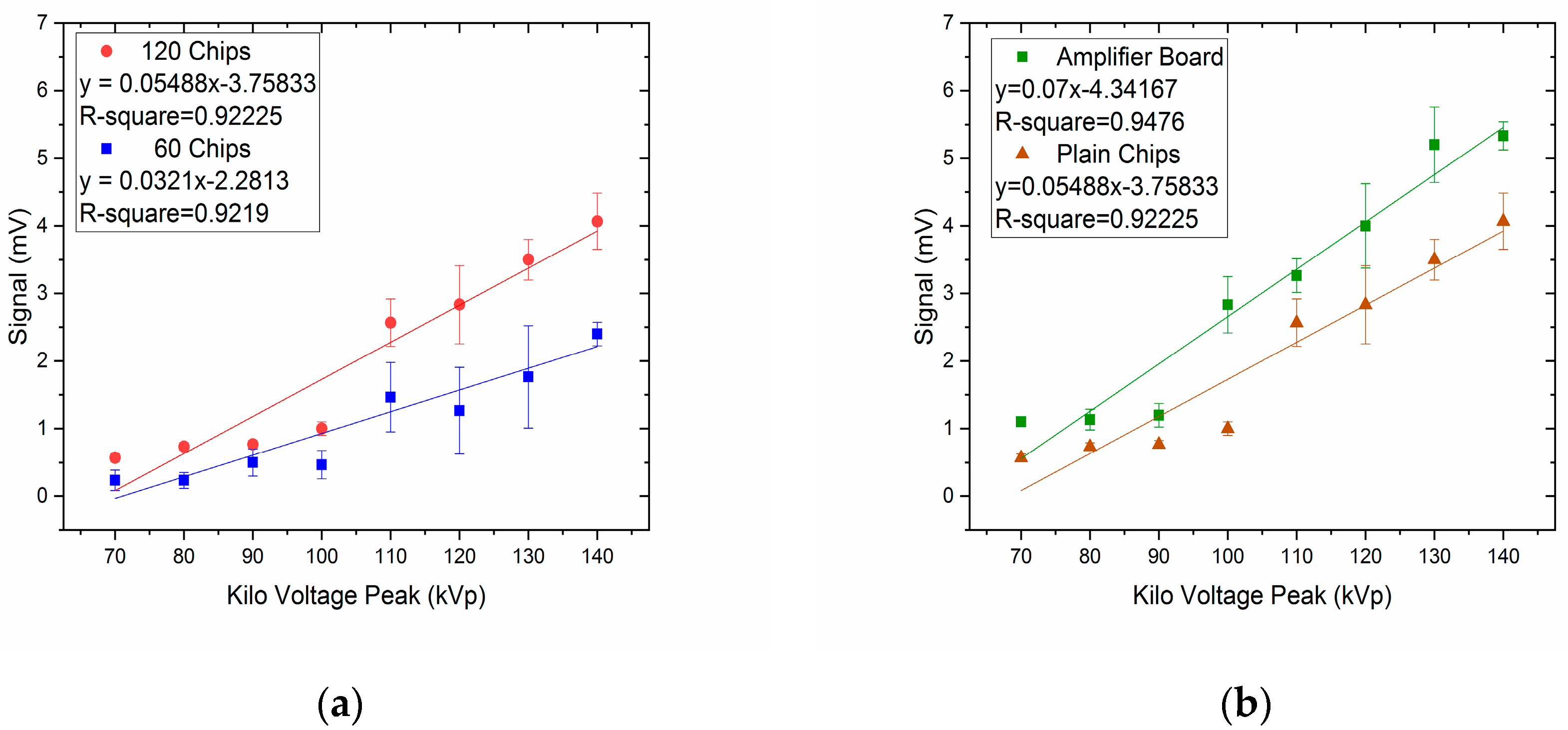
3.3. Amplification during Tube Voltage (kVp) Variation

The linearity coefficient of the signal to kVp variation was 0.9219 when the active area was 756 mm2 (60 chips). The signal that was obtained per unit tube voltage was 0.0321 mV/kVp. Increasing the active area to 1512 mm2 (120 chips) led to a 0.04% increment in the linearity coefficient of the signal to kVp variation; hence, the linearity coefficient slightly increased to 0.92225. Likewise, the signal that was obtained per unit tube voltage increased from 0.0321 to 0.05488 mV/kVp, which implied a 70.97% increment in mVs obtained per kVp. Therefore, during kVp alteration, there was a 0.09% increase in the mV/kVp for each mm2 of active area increment, as observed in Figure 6a.
Amplifications using the amplifier board produced a 2.75% increase in the signal’s linearity during kVp alteration; thus, the linearity coefficient increased from 0.92225 to 0.9476. The signal detected per unit kVp increased from 0.05488 to 0.07000 mV/kVp, hence a 27.55% mV/kVp increase. Therefore, for kVp alterations, there was a 2.755 × 10⁻⁸% increase in the mV/kVp for each voltage gain by the amplifier board, as observed in Figure 6b.

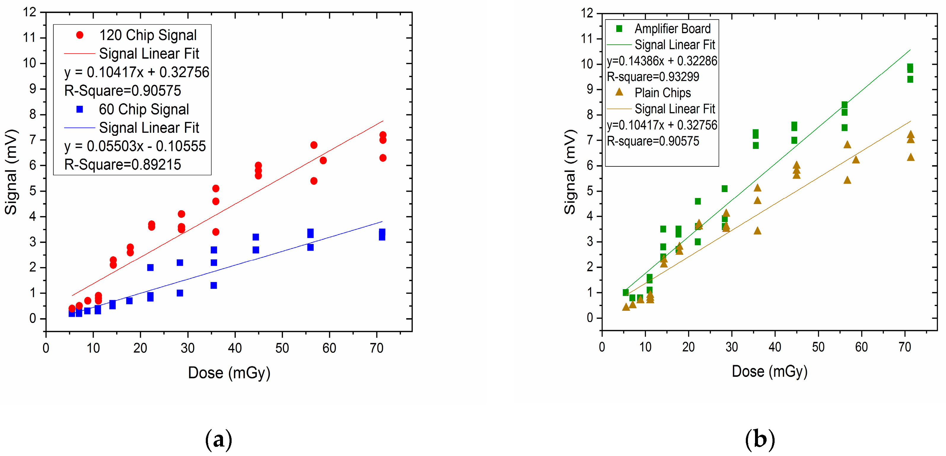
3.4. Amplification during Absorbed Dose Variation

The signal that was collected by an active area of 756 mm2 (60 chips) was 89.23% linear to dose. The sensitivity that was attained with this area was 0.05503 mV/mGy. Nonetheless, the signal obtained with an active area of 1512 mm2 (120 chips) was 90.58% linear to dose, hence a 1.52% increment in signal linearity to dose—as a result of increasing the active area by 756 mm2. Similarly, there was an 89.3% increase in the sensitivity, i.e., the sensitivity increased from 0.05503 mV/mGy to 0.10417 mV/mGy. Therefore, a 1 mm2 increase in the active area resulted in a 0.002% and a 0.12% linearity to dose and sensitivity increase, respectively, as in Figure 7a.
On the other hand, there was a 3.01% reduction in the linearity of the signal to dose when the amplifier board was applied for signal amplification. Nevertheless, sensitivity increase of 38.10% was observed; thus, the sensitivity increased from 0.10417 mV/mGy to 0.14386 mV/mGy. Therefore, amplification while using the amplifier board produced a 3.01 × 10⁻⁹% reduction in the signal linearity to dose for every voltage gain. Nonetheless, every voltage gain produced a 3.81 × 10⁻⁸% increase in the sensitivity to dose, as illustrated in Figure 7b.

3.5. Amplification during Source-To-Detector Distance (SDD) Variation

Increasing the SDD resulted in a signal fade with an exponential decay fit coefficient of 0.99781, when the detecting active area was 756 mm2 (60 chips). However, as a consequence of increasing the active area by 756 mm2 (60 chips), the exponential decay fit coefficient was reduced by 1.12%, thus a shift of the decay fit coefficient from 0. 99781 to 0.98668.
With a detecting active area of 756 mm2 (60 chips), the signal faded at a rate of 3.348 mV/cm, at the minimum SDD (60 cm). At the maximum SDD (90 cm), the signal fading rate reduced to 1.033 mV/cm. When the detecting active area was increased to 1512 mm2 (120 chips), the signal faded at rates of 6.680 and 2.118 mV/cm at SDDs of 60 and 90 cm, respectively (Figure 8a). Therefore, at SDDs of 60 and 90 cm, 99.52%, and 105.03%, increases in the signal fading rate were respectively observed; this was due to an increase in the active detecting area by 756 mm2 (60 chips).
The amplifier board output signal had a signal fading rate of 9.399 mV/cm at 60 cm and 2.945 mV/cm at 90 cm of SDD. This implied a 40.70% and 39.05% increase in the signal fading at SDDs of 60 cm and 90 cm, respectively.

3.6. Summary of Signal Amplification

Table 1 illustrates a discrete analysis of the active area and amplifier board percentage gains that were observed in Section 3.1, Section 3.2, Section 3.3, Section 3.4 and Section 3.5. From the table, the active area amplification mode yielded an average signal augmentation of 91.16% across the four X-ray parameter variations. On the other hand, the amplifier board amplification mode yielded a signal augmentation of 36.48% for the tested X-ray parameters in this study.

3.7. Coefficients of Variation (CoVs) during Signal Amplification

The signals that were obtained during chip number-based signal amplifications were characterized with an average of 8.737% coefficient of variation throughout all the mAs, kVp, and SDD X-ray parameter variations. Amplifier board output signals also had an average coefficient of variation of 9.424% across the mAs, kVp and SDD parameter variations, as illustrated in Table 2.

4. Discussion

Amplifications were implemented under varying tube voltage (kVp) and tube current-time product (mAs) conditions, owing to kVp and mAs being fundamental X-ray machine settings that are correlated to X-ray absorbed doses [20,21]. In other words, radiation-induced signals as a result of tube voltage and tube current-time product alteration were amplified. All the amplified signals were linear to the tube current-time product (mAs) and tube voltage (kVp), similar to Huda [22] and Chiara’s [5] work.
Tube current-time product (mAs) is a tube setting that regulates the X-ray beam’s population (number of photons in the X-ray beam) [14]. During mAs variation, Figure 5a shows a 3.49% decrease in the signal linearity coefficient (R-square) when the chip number was increased from 60 to 120. In this case, the R-square signifies the extent to which the signal data points conform to the linear fitting during mAs variation. When the chip number was doubled to 120 chips, it could be considered that there was no change in the linearity coefficient (the change was trivial). This is because only a 3.49% change was observed, and this change is below the 5% uncertainty (95% confidence interval) [23].
Additionally, amplification of different radiation intensity-induced signals was realized with SDD variation. The detected signals during SDD variation highly conformed to the exponential decay fit, because radiation intensity reduces in the form of an exponential decay graph, as the distance from the radiation source (SDD) is increased. This exponential decay conforms to the Lambert-Beer Law [11,24], I = I0E(−kx), where I0 is the initial radiation intensity and I is the radiation intensity after the radiation travels a distance x through a medium with an absorption coefficient constant k.
PIN photodiode active area is directly proportional to the collected signal, because the radiation-induced current (ID) is equivalent to the product of the PIN photodiode constant (k), active area (A), depletion layer width (w), and the incident radiation’s dose rate (DR), i.e., ID = kAwDR [25]. However, the magnitudes of k, A, and w are predetermined by the transducer manufacturer. Therefore, users cannot expand the transducer intrinsic active area size. Nonetheless, the effective active area could be increased by connecting multiple sole transducers in the form of an array.
LED active area is directly proportional to the detected signal when applied as a radiation detector because LEDs could be assumed as photodiodes that do not detect, but rather emit light. For this reason, active area increment yielded higher signal amplification results and a high signal gain per mm2 increase in active area in our study. Anđelković [6] similarly highlighted active area to be directly correlated to photodiode sensitivity towards radiation; this likewise implies a proportionate signal build up in case of active area increment. The LED radiation signal was amplified by increasing the chip number because connecting multiple photodiodes in parallel can enhance photodiode effective active area and sensitivity [6].
However, during the active area-based amplification mode, the highest signal per mm2 increase in the active area was observed in the course of visible light detection, because LEDs feasibly detect wavelengths that are similar to those they emit [15]. Therefore, active area increment-based signal amplifications were most effective during visible light detection. This finding further implies that the LED’s low signal set-back, during light detection, could be offset by increasing the effective sensitive area: Hence, LEDs could substitute photodiodes during light detection applications, due to their low-cost and flexibility when compared to photodiodes.
Whereas Anđelković [6] applied transimpedance amplifiers to amplify low photodiode radiation-induced signals, our study executes electronic signal amplification with an amplifier board. Nevertheless, the board was presented with low signal amplification percentages throughout the tested X-ray parameter variations. Amplifier board settings could be adjusted to higher gains, but this was coupled with higher dark currents. These amplifier board pre-existent dark currents would ultimately obstruct precision in the measurement of net radiation-induced currents/signal amplifications. Amplified signals should additionally be precise and have low standard deviations because precise signals ensure accurate dosimetric calibrations. Herein, we examined amplified signal precision while using the coefficient of variation (CoV) tool, which is the percentage of the standard deviation (σ) to mean (μ) ratio, i.e., CoV = σ/μ×100%. Amplifier board signals had a 0.687% (9.424%–8.737%) higher coefficient of variation than the chip number-based signal amplifications; this could be as a result of amplifier board dark currents that might have hindered precise signal measurement. Additionally, the amplifier board’s maximum usable output voltage was ±4 V, which could imply a limited operational headroom. As a consequence, whilst adjusting the potentiometers to achieve low dark currents, the amplifier board easily got saturated to an output voltage of ~4.24 V.
Variation in the temperature surrounding the LED chips could lead to changes in the LED emission spectrum and emitted wavelengths: LED efficacy as a luminary reduces upon an increase in temperature [26]. The semiconductor material that is used for LED fabrication dictates LED bandgap energy and, ultimately, the energy of the emitted light photons [27]. This bandgap energy (Eg) is directly proportional to the speed of light-C and inversely proportional to emitted photon wavelength-λ with Plank’s constant-h as the constant of proportionality, i.e., Eg = hC/λ. An increase in temperature would reduce Eg because Eg is the energy difference between valence and conduction bands [2], thus an increase in the emitted photon wavelength. Therefore, data collection from our experiments was executed in a radiology suite with room temperature being maintained at 24 °C. This testing condition minimized the signal-temperature dependence that could affect the sensibility of the LEDs implemented for diagnostic X-ray radiation detection herein. Although the efficiency of LEDs is a function of LED PN junction temperature, InGaN-based LEDs (for instance, blue, green, white) are less ambient-temperature dependent [28]. Heat sinks are also constructed around LED active area structures to further buffer the temperature dependence effects.
Temperature can reduce the efficiency of an LED as a light emitter, particularly when it is used for a long time. However, in the reverse function, i.e., in the detection of X-rays, the processing time (X-ray exposure time) is very short (in milliseconds), hence the temperature factor could be negligible. Therefore, based on these latter considerations, we assumed the temperature around the LED active areas would not increase due to X-ray absorption.
All in all, active area-based amplification was simple, direct, and, above all, inexpensive—in comparison to the amplifier board that was quite costly (~100 €) and was associated with some limitations such as dark currents and saturation. Despite these setbacks, a hybrid amplification mode, amalgamating both the amplifier board and active area amplifications, would be a prospective amplification modal with summed advantages. Alternatively, amplifier boards with higher operating output voltage, low dark currents, and low saturation possibilities would be employed for higher electronic amplification gains. Additionally, LEDs of different emission wavelength spectrums [29] could also possibly be another signal amplification option to exploit because LEDs detect photons with a wavelength that is similar to the one that they emit [15].
In this survey, we implemented cold white LED strips, because they were presented with a better dosimetric performance as compared to the warm white, red, green, and blue LED strip colors in our prior survey [14]. Future work could, however, explore diagnostic X-ray detection using other LEDs colors, for instance, ultraviolet (UV) LEDs.
Herein, heating effects, which may arise from the interaction between the X-rays and LED PN junction, were negligible. The impact of such effects on the generated photovoltaic signal might also be explored and quantified in future studies.
From Section 3.1, LEDs demonstrated high sensitivity to visible light photons. Future studies could, therefore, convert the X-rays to visible light using scintillators. The visible light photons emitted from these scintillators could then be detected using LEDs.
LEDs fabricated using higher atomic mass semiconductor material could also similarly produce higher X-ray radiation-induced signals since higher atomic mass semiconductors are generally associated with higher X-ray photon absorption capabilities [30]. However, this could be associated with higher dark currents due to the shorter bandgap of these high atomic mass materials [30]. In this event, charge localized in valance traps can easily jump over the short bandgap, after ambient energy absorption, hence excitation that implies a dark current.

5. Conclusions

The amplification of diagnostic X-ray radiation-induced signals of LED strip was accomplished by increasing the LED strip effective active area and by injecting the LED raw signal into an amplifier board—mainly consisting of transistors, transimpedance, and operational amplifiers. Amplification by increasing the active area produced high amplification coefficients, whereas the amplifier board amplification coefficients were lower than the latter. The amplification techniques both produced consistent results in the amplification of signals induced by the range of tube voltages (kVp), tube current-time product (mAs), and source-to-detector distance (SDD) tested in this study.
Therefore, this work has initiated and established a platform for further and detailed LED radiation-induced signal analysis. This would attract more implementation of LEDs for X-ray detection purposes.
In a nutshell, the diverse signal amplification techniques that were outlined in this work ultimately depict LEDs as novel and promising radiation detectors that could be potentially exploited for X-ray beam dosimetry in both diagnostic radiology and radiation protection fields.

Author Contributions

Conceptualization, E.D. and M.N.S.Y.; Data curation, E.D. and M.N.S.Y.; Formal analysis, E.D. and M.N.S.Y.; Funding acquisition, M.N.S.Y.; Investigation, E.D.; Methodology, E.D. and M.N.S.Y.; Project administration, M.N.S.Y.; Resources, M.N.S.Y. and A.F.O.; Supervision, M.N.S.Y., A.F.O. and N.H.M.T.; Validation, E.D. and M.N.S.Y.; Visualization, E.D.; Writing—original draft, E.D.; Writing—review & editing, E.D., M.N.S.Y., A.F.O. and N.H.M.T. All authors have read and agreed to the published version of the manuscript.

Funding

This research was funded by the Short-Term Grant, Universiti Sains Malaysia, Grant No. 304/PPSK/6315117.

Acknowledgments

The authors would like to thank the Department of Radiology, Hospital Universiti Sains Malaysia (HUSM) for giving the permission to use the X-ray equipment and providing necessary technical resources during the execution of experiments.

Conflicts of Interest

The authors declare no conflict of interest.

References

  1. Remello, S.N.; Hirano, T.; Kuttassery, F.; Nabetani, Y.; Yamamoto, D.; Onuki, S.; Tachibana, H.; Inoue, H. Visible light induced oxygenation of alkenes with water sensitized by silicon-porphyrins with the second most earth-abundant element. J. Photochem. Photobiol. A Chem. 2015, 313, 176–183. [Google Scholar] [CrossRef]
  2. Damulira, E.; Yusoff, M.N.S.; Omar, A.F.; Taib, M.; Hartini, N. A Review: Photonic Devices Used for Dosimetry in Medical Radiation. Sensors 2019, 19, 2226. [Google Scholar] [CrossRef] [PubMed] [Green Version]
  3. Ciarrocchi, E.; Belcari, N. Cerenkov luminescence imaging: Physics principles and potential applications in biomedical sciences. EJNMMI Phys. 2017, 4, 14. [Google Scholar] [CrossRef] [PubMed] [Green Version]
  4. Yatsu, Y.; Kuramoto, Y.; Kataoka, J.; Kotoku, J.; Saito, T.; Ikagawa, T.; Sato, R.; Kawai, N.; Kishimoto, S.; Mori, K.; et al. Study of avalanche photodiodes for soft X-ray detection below 20 keV. Nucl. Instrum. Methods Phys. Res. Sect. A Accel. Spectrometers Detect. Assoc. Equip. 2006, 564, 134–143. [Google Scholar] [CrossRef]
  5. Romei, C.; Di Fulvio, A.; Traino, C.A.; Ciolini, R.; d’Errico, F. Characterization of a low-cost PIN photodiode for dosimetry in diagnostic radiology. Phys. Med. 2015, 31, 112–116. [Google Scholar] [CrossRef]
  6. Anđelković, M.S.; Ristić, G.S. Feasibility study of a current mode gamma radiation dosimeter based on a commercial PIN photodiode and a custom made auto-ranging electrometer. Nucl. Technol. Radiat. Prot. 2013, 28, 73–83. [Google Scholar] [CrossRef]
  7. Bryant, J. Photodiodes and Other Light Sensors. 2014. Available online: https://www.analog.com/cn/index.html# (accessed on 10 December 2018).
  8. Zhao, S.; Lioliou, G.; Barnett, A. Temperature dependence of commercial 4H-SiC UV Schottky photodiodes for X-ray detection and spectroscopy. Nucl. Instrum. Methods Phys. Res. Sect. A Accel. Spectrometers Detect. Assoc. Equip. 2017, 859, 76–82. [Google Scholar] [CrossRef]
  9. Kester, W.; Bryant, J.; Jung, W.; Wurcer, S.; Kitchin, C. Sensor signal conditioning. Sens. Technol. Handb. 1999, 2, 31–136. [Google Scholar]
  10. Zygmanski, P.; Abkai, C.; Han, Z.; Shulevich, Y.; Menichelli, D.; Hesser, J. Low-cost flexible thin-film detector for medical dosimetry applications. J. Appl. Clin. Med. Phys. 2014, 15, 311–326. [Google Scholar] [CrossRef]
  11. Bui, D.A.; Hauser, P.C. Absorbance measurements with light-emitting diodes as sources: Silicon photodiodes or light-emitting diodes as detectors? Talanta 2013, 116, 1073–1078. [Google Scholar] [CrossRef]
  12. Tymecki, Ł.; Brodacka, L.; Rozum, B.; Koncki, R. UV-PEDD photometry dedicated for bioanalytical uses. Analyst 2009, 134, 1333–1337. [Google Scholar] [CrossRef] [PubMed]
  13. Tymecki, Ł.; Pokrzywnicka, M.; Koncki, R. Paired emitter detector diode (PEDD)-based photometry—An alternative approach. Analyst 2008, 133, 1501–1504. [Google Scholar] [CrossRef] [PubMed]
  14. Damulira, E.; Yusoff, M.N.S.; Sulaiman, S.; Zulkafli, N.F.H.; Zulkifli, N.A.; Shakir, N.S.A.; Zainun, M.A.; Omar, A.F.; Taib, N.H.M.; Ali, N.K.Y. Comparison of Current–Voltage Response to Diagnostic X-rays of Five Light-Emitting Diode Strips. Appl. Sci. 2020, 10, 200. [Google Scholar] [CrossRef] [Green Version]
  15. Mims, F.M. Sun photometer with light-emitting diodes as spectrally selective detectors. Appl. Opt. 1992, 31, 6965–6967. [Google Scholar] [CrossRef] [PubMed]
  16. Beringer, J.; Borer, K.; Mommsen, R.K.; Nickerson, R.B.; Weidberg, A.R.; Monnier, E.; Hou, H.Q.; Lear, K.L. Radiation hardness and lifetime studies of LEDs and VCSELs for the optical readout of the ATLAS SCT. Nucl. Instrum. Methods Phys. Res. Sect. A Accel. Spectrometers Detect. Assoc. Equip. 1999, 435, 375–392. [Google Scholar] [CrossRef] [Green Version]
  17. Dowell, J.D.; Homer, R.J.; Kenyon, I.R.; Mahout, G.; Oglesby, S.J.; Shaylor, H.R.; Wilson, J.A.; Nickerson, R.B.; Wastie, R.; Weidberg, A.R. Irradiation tests of photodiodes for the ATLAS SCT readout. Nucl. Instrum. Methods Phys. Res. Sect. A Accel. Spectrometers Detect. Assoc. Equip. 1999, 424, 483–494. [Google Scholar] [CrossRef] [Green Version]
  18. Li, Z.; Feng, B.; Deng, B.; Liu, L.; Huang, Y.; Feng, M.; Zhou, Y.; Zhao, H.; Sun, Q.; Yang, X. Light output improvement of GaN-based light-emitting diodes grown on Si (111) by a via-thin-film structure. J. Semicond. 2018, 39, 044002. [Google Scholar] [CrossRef]
  19. Farnell, P. Multifunctional 2-Channel Amplifier Board Leeds; Farnell: Leeds, UK, 2019; Available online: https://www.farnell.com/datasheets/65044.pdf (accessed on 15 March 2019).
  20. Kubo, T.; Lin, P.J.P.; Stiller, W.; Takahashi, M.; Kauczor, H.U.; Ohno, Y.; Hatabu, H. Radiation dose reduction in chest CT: A review. Am. J. Roentgenol. 2008, 190, 335–343. [Google Scholar] [CrossRef]
  21. Riederer, I.; Zimmer, C.; Pfeiffer, D.; Wunderlich, S.; Poppert, H.; Rummeny, E.J.; Huber, A. Radiation dose reduction in perfusion CT imaging of the brain using a 256-slice CT: 80 mAs versus 160 mAs. Clin. Imaging 2018, 50, 188–193. [Google Scholar] [CrossRef]
  22. Huda, W.; Sajewicz, A.M.; Ogden, K.M.; Dance, D.R. Experimental investigation of the dose and image quality characteristics of a digital mammography imaging system. Med. Phys. 2003, 30, 442–448. [Google Scholar] [CrossRef]
  23. Mitch, M.G.; De Werd, L.A.; Minniti, R.; Williamson, J.F. Treatment of Uncertainties in Radiation Dosimetry; Medical Physics Publishing: Madison, WI, USA, 2009. [Google Scholar]
  24. Mazda, F. Telecommunications Engineer’s Reference Book; Butterworth-Heinemann: Oxford, UK, 2014; ISBN 1483193799. [Google Scholar]
  25. Lanza, J.J.; Mauderli, W.; Fitzgerald, L.; Roessler, G. An Automated Dosimetry System For Computed Tomography X-ray Scanners Using Silicon Pin Diodes.: P/63. Health Phys. 1980, 39, 1020. [Google Scholar] [CrossRef]
  26. Choi, H.-W.; Choi, M.H.; Ko, J.-H. Effect of temperature on the luminous properties of white-light-emitting diodes with red and green phosphors. New Phys. Sae Mulli. 2013, 63, 1149–1154. [Google Scholar] [CrossRef]
  27. Gayral, B. LEDs for lighting: Basic physics and prospects for energy savings. Comptes Rendus Phys. 2017, 18, 453–461. [Google Scholar] [CrossRef]
  28. NLPIP. How Are LEDs Affected by Heat? New York, United States National Lighting Product Information Program. Available online: https://www.lrc.rpi.edu/programs/nlpip/lightinganswers/led/heat.asp (accessed on 4 January 2020).
  29. Paschotta, R. Light-Emitting Diodes. The Encyclopedia of Laser Physics and Technology 2008. Available online: https://www.rp-photonics.com/light_emitting_diodes.html (accessed on 7 April 2018).
  30. Duboz, J.Y.; Lauegt, M.; Schenk, D.; Beaumont, B.; Reverchon, J.L.; Wieck, A.D.; Zimmerling, T. GaN for x-ray detection. Appl. Phys. Lett. 2008, 92, 263501. [Google Scholar] [CrossRef]
Figure 1. Experimental Setup: (a) Schematic of the Irradiation Set-up and (b) Masked LED strips on a solid water phantom.
Applsci 10 00651 g001
Figure 2. Signal Amplification by LED chip number/active area increment. Note: This image only shows how the LED strips were reconnected successively—it was taken when five strips were reconnected. During the experiments, the number of LED strips (active area) reconnected was as stated in the different sections of this report.
Applsci 10 00651 g002
Figure 3. Signal Amplification using an Amplifier Board: (a)-Image of the amplifier board, (b)-Schematic of the amplifier board circuitry (extracted from [19]).
Applsci 10 00651 g003
Figure 4. A graph of signal gain due to LED chip number/sensitive area increment.
Applsci 10 00651 g004
Figure 5. A graph of signal augmentation with (a) Number of LED chips/sensitive area and (b) Amplifier Board amplification; during tube loading variation (mAs).
Applsci 10 00651 g005
Figure 6. A graph of signal augmentation with (a) Number of LED chips/sensitive area and (b) Amplifier Board amplification, during tube voltage variation (kVp).
Applsci 10 00651 g006
Figure 7. A graph of signal augmentation with (a) Number of LED chips/sensitive area and (b) Amplifier Board amplification; with respect to absorbed dose variation (mGy).
Applsci 10 00651 g007
Figure 8. A graph of signal augmentation with (a) Number of LED chips/sensitive area and (b) Amplifier Board amplification; during source-to-detector distance variation (cm).
Applsci 10 00651 g008
Table 1. Percentage Signal Variation Per Unit X-ray Parameter.
Signal Amplification ModeX-ray Beam Parameter
Tube current-time product (mV/mAs)Tube Voltage (mV/kVp)Dose (mV/mGy)Source-to-Detector Distance, SDD (mV/cm)
60 cm90 cm
Percentage Signal Increase (%)Percentage increase in Signal Fading (%)
Chip number increment from 60 to 120 chips90.9970.9789.3099.52105.03
Amplifier Board with a gain of 109 V/A36.9927.5538.1040.7039.05
Table 2. Signal coefficient of variation (CoV) associated with each amplification mode.
Amplification ModeCoV for Each X-ray Beam ParameterAverage CoV
Tube current-time product—mAs (%)Tube Voltage—kVp (%)Source-to-Detector Distance—SDD (%)Based on each amplification mode (%)
Chip number increment from 60 to 120 chips6.16711.0588.9878.737
Amplifier Board with a gain of 109 V/A9.02810.0679.1779.424

