1. Introduction
The interaction between electromagnetic waves, for instance light, and matter was always a topic that aroused interest to the scientific community [
1,
2,
3,
4]. Mainly because some phenomena were discovered recently, as the extraordinary optical transmission (EOT) and based on them it has been possible to develop new devices [
1,
2,
5,
6].
The resonant behavior characteristic from EOT is affected by the complex dielectric function, which also depends on the incident wavelength. The complex dielectric function is often presented as a fitting of the Drude–Lorentz model, for each material [
1,
2,
7,
8].
The variation of the complex dielectric function with physical or chemical events can be useful to develop a sensor. This kind of sensors can be designed for many application in different fields such as medicine, chemistry, defense, communications, energy or environment [
1,
2,
6].
A nanoantenna, which is a subwavelength hole structure that supports EOT, can be tuned and its material can be chosen in order to fulfill spectral specifications (for example, gain, bandwidth or peak position). Thus, it is possible to design the sensor optical response [
1,
2,
9,
10,
11,
12,
13,
14,
15,
16,
17,
18,
19,
20].
It is expected that this new kind of sensor, in the near future, will be classified as standalone, miniaturized, portable and they will have high sensibilities and huge detection limits [
1,
2,
17,
18,
19,
20]. However, the improvement of computational methods and of new techniques of manufacturing are leading the process of creating new nanotechnological devices. Thus, sensors based on nanoantennas are not exceptions and they are quite important factors to decrease the fabrication costs and increase the reproducibility and the probability to commercialize these devices [
6,
17,
18,
19,
20]. It is needed to find models to be able to clarify how the spectrum changes regarding the parameters tuning [
1,
2,
21,
22,
23,
24,
25,
26,
27]. This article not only aimed to analyze the parameter influence, but it also presents simulations from two different sensor applications.
2. Evolution of the Theoretical Foundations
Since the XVII century, based on experimental works, theories have been proposed to explain light behavior, namely when interacting with matter. [
1,
3,
4]. In this century, Huygens stated that each unobstructed point from a plane wave front can be analyzed as a punctual source, emitting a spherical wave with the same characteristics from the main (real), wave [
1,
3,
4]. However, only in the XVIII century, Fresnel reformulated the Huygens principle in order to explain the rectilinear propagation of light and diffraction effects. This was a huge progress, because it aims on the study of the near-field regime. To assume a plane wave, the distance between the source and the target, where the analysis is performed, should be very large and, in this condition, geometrical optics methods can aim to analyze the wave propagation [
1,
3,
4].
In the beginning of the XIX century, Young proved the wave characteristic of light, using a double slit experiments and the Huygens–Fresnel principle [
1,
3,
4].
Fraunhofer also used the Huygens principle to compose his diffraction theory, that relates the irradiance at a certain angle of diffraction
and the main lobe one (
), after the wave propagates though a slit in a metallic plane. Nonetheless, as presented in expression (
1), for N slits, the relation is between the irradiance at a certain angle and an irradiance
, that is the contribution of each equal slit for the overall irradiance [
1,
3,
4,
6]. However, he assumed a plane and monochromatic wave, characterized by an incident wavelength
and a wavevector
, with perpendicular incidence to a perfect conductive metal, with N slits of diameter
a and spaced by a distance
d [
1,
3,
4,
6]. The analysis target is over the slits plane, at a distance
D and the distance between the plane position given by
and the main lobe one is given by y [
1,
3,
4,
6]. Fraunhofer determine the maximum and the minimum intensity positions, y, on the target, regarding the constructive and destructive interference among different rays propagating from the slits plane [
1,
3,
4,
6]. Expressions (2) and (3) are obtained using these distance definitions and under the far-field assumption (
) [
1,
3,
4,
6].
After that, Kirchhoff composed his theory, that includes as limit cases the Fresnel and Fraunhofer’s theories [
1,
6,
28]. He assumed the propagation of a plane and scalar wave along the
x direction and an opaque plane perpendicular to it [
1,
6,
28]. The opaque plane has an aperture and the transmitted wave propagation is determined by expression (
4), that degenerates expression (
5), using Green’s theorem [
1,
28]. The scalar wave is
and the integration coordinates should be
and
, such as
,
and
are the coordinates of a point
before or over the metal surface. Moreover,
is the Green’s function, for a monochromatic wave at a point
after the plane, given by
.
However, boundary conditions are not verified at the metal surface on Kirchhoff’s theory, since he assumed an opaque and finite plane [
1,
6,
28]. As the incident and reflected waves do not exist over the surface, these conditions are not satisfied, especially on the surfaces near the slits [
1,
28]. For subwavelength structures and for the near-field regime, this problem can not be neglected. Thus, in 1944, Bethe presented his theory, assuming an infinite and perfect conductive metal plane with a circular hole [
6,
28]. Bethe’s goal was to improve Kirchhoff’s theory, fulfilling the boundary conditions. However, years later, Bouwkamp showed that Bethe’s equations do not verify it and he amended it, using the Babinet’s principle [
1,
6,
29]. Expressions (
6) and (
7) are the Bouwkamp’s results from the electric and the magnetic vectors, when the wave propagation is on the
z direction [
1,
6,
29]. Nonetheless, Bethe showed, and Bouwkamp reformulated the expressions, but he took the same conclusions, that hole structures can behave as an electric and a magnetic dipole and, using Poynting’s theorem, it is possible to determine the complex radiation power. When applying the subwavelength hole condition to this expression, its results show that the radiation power decay should be proportional to
[
1,
6,
28,
29].
3. Surface Plasmon Polaritons and the Extraordinary Optical Transmission
In 1998, Ebbesen reported that nanostructures, composed by periodic circular holes, can amplify and concentrate electromagnetic radiation [
5]. These structures, also known as nanoantennas, allow an unexpected transmission spectrum. This phenomenon was called extraordinary optical transmission and Ebbesen stated that its main agents are the surface plasmon polaritons [
1,
5]. Classical theories cannot predict this phenomenon, since it is possible to amplify light using a structure with nano holes. Two conditions are fundamental to the excitation of polaritons, considering that the metal has a complex dielectric function given by
and the dielectric medium is characterized by a real function
: (i)
and
; (ii) a match between the wavevector of the polariton and the parallel component one of the incident light with the interface [
1,
2,
6,
30,
31,
32,
33].
Years later, Lalanne e Hugonin did an analytical study from Maxwell’s equations that proved the propagation of surface plasmon polaritons, as a fundamental stage for this phenomenon, as well as its combination with a creeping wave propagation [
33].
In the 1950s, the interest in plasmons received a great impulse with the works of Pines and Bohm. Later, in 1956 Fano introduces the concept of polariton and in 1957 Ritchie presented the first theoretical description of surface plasmons. Surface plasmon polaritons TM propagation equations are presented on expression (
8), for a surface at
, where there is metal/plasma for
and dielectric for
[
1,
6,
30,
31,
32]. Thus, the plane is extended along the
y-axis and there are oscillations along
x and an exponential decay over the
z-direction.
A plasmon is the redistribution of the plasma’s free electrons, a quantum of a plasma oscillation [
1,
6,
30,
31,
32,
33]. Light is also an oscillation of particles, in this case the photons. Both oscillations can couple and in this case the polariton is created. A polariton, a quasiparticle as the plasmon is, is the result of a strong coupling between an electromagnetic wave (light in this case), and an electric or magnetic dipole (the nanoantenna as verified by Bethe’s and Bouwkamp’s theories) [
1,
6,
28,
29,
30,
31,
32]. This energy exchange is a resonant behavior, capable to amplify and concentrate electromagnetic energy near the surfaces.
When extraordinary optical transmission was discovered by Ebbesen, he sooner reported that this resonant behavior can be useful to develop a new type of miniaturized photonic devices, as optical sensors [
1,
2,
5].
However, new studies reported EOT at frequencies where the surface plasmon polaritons cannot be generated or in materials that do not fulfill the conditions to excite these polaritons [
33,
34,
35,
36,
37]. Thus, their role, in other frequencies out of the visible and near-infrared spectral regions or for othermaterials than metals, is taken by other waves propagation, as creeping and leaky waves [
33,
38,
39].
The behavior of nanoantennas has already been modeled using electronic circuits, based on frequency-selective surfaces, waveguides and transmission lines theories [
37]. These models give an interpretation of EOT in terms of impedance matching [
37]. As any equivalent circuit, they have some advantages since they are simpler to study and understand.
4. Structure Parameters Evaluation
This article will show the resonant behavior of the EOT, as well as the capability of amplify and concentrate electromagnetic radiation, for a metallic nanoantenna at frequencies on the visible and near-infrared spectral regions. This research work proves that it is possible to design a optical sensor using its resonant properties. The first step to develop a structure is to try to understand how its parameters can influence the output spectrum [
2]. This article aimed to find new nanostructures that can work as sensors. For that reason, parameters are studied, before simulating a structure as a sensor, in order to verify how the structure optical response can be tuned, considering the same simulation environment, inputs, methods and simulation conditions. Thus, materials were modeled by the same type of fitting, boundary conditions are always the same and well defined, as well as the measurement conditions (that leads to the following spectra).
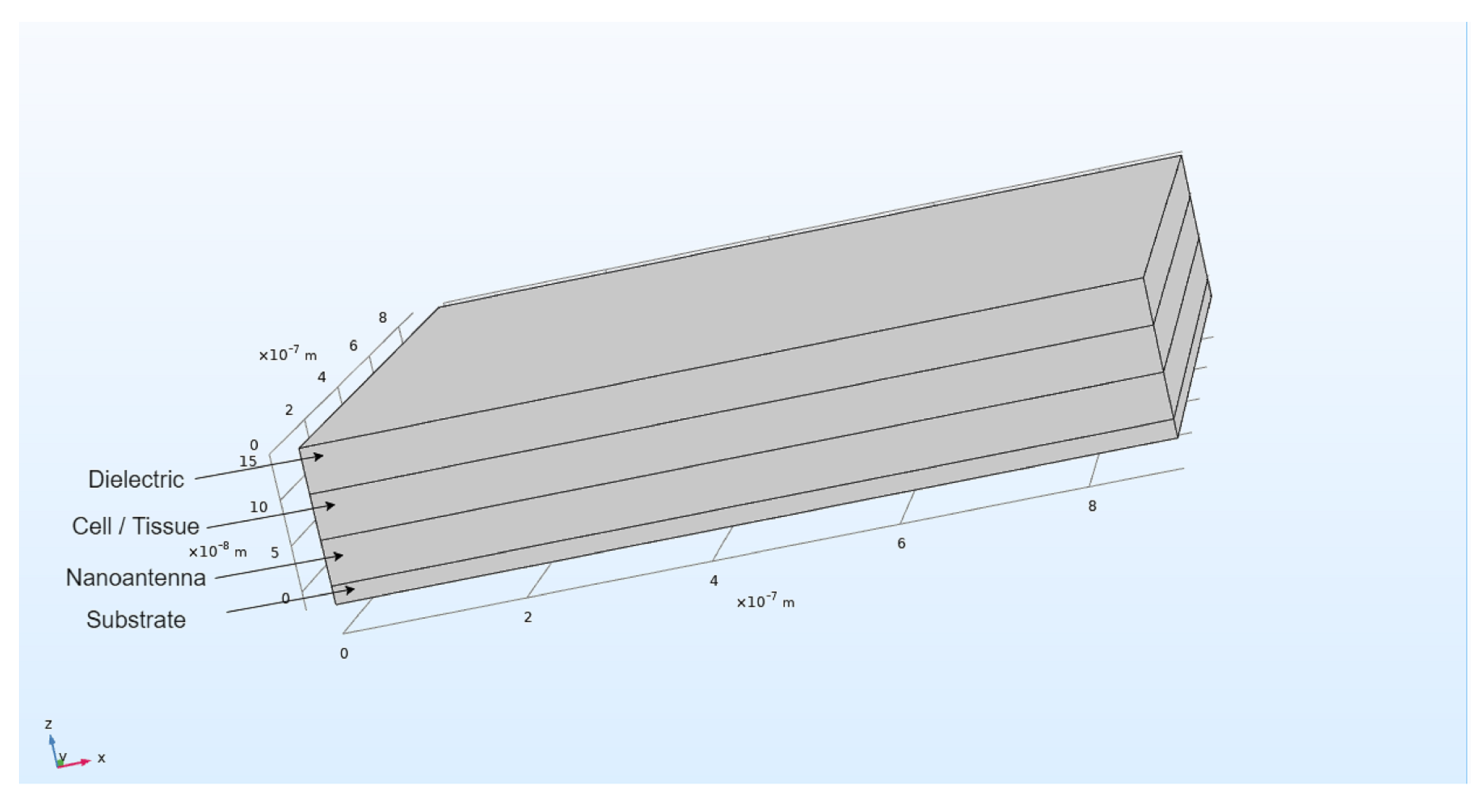
Several simulations were performed in order to verify the variation of the spectral response regarding parameter sweeps (periodicity, hole diameter, nanoantenna thickness and substrate thickness) [
2,
9,
11,
12,
14,
18,
22]. These sweeps are done based on a reference structure and are presented in
Figure 1. It is a 3 × 3 squared array structure, composed by circular holes and characterized by a periodicity of
, a hole diameter of
, a nanoantenna thickness of
, as well as a substrate thickness of
. In addition, the dielectric medium has a thickness of
; however, it is measured from the interface between the nanoantenna and the substrate in order to set the hole medium as dielectric [
2].
An electric field, defined by a norm of
, is generated on the top of the structure presented in
Figure 1 (that is on the external boundary of the dielectric medium) and its perpendicularly incident is on the nanoantenna, having the
z-axis opposite direction. Thus, on the generation port, this electric field was defined as
and
. Furthermore, all the external boundaries are total absorbent, meaning that there is no reflection.
Moreover, all the simulations are done for 250 equidistant wavelength points, from to . The frequency analysis is done using a boundary probe (on/under the substrate) and measuring the square of the maximum ratio between the electric field norm and the incident electric field norm, .
All the spectra that will be presented are only possible to reach due to the generation and propagation of surface plasmon polaritons, near the interfaces, as it is possible to visualize in
Figure 2 [
2], for metal made nanoantennas and at frequencies on the visible and near-infrared regions. In this figure, it is quite noticeable that in these regions, there is field amplification, because the electric field norm is higher than the incident one [
2].
In this article, a structure composed by an air dielectric medium and a quartz substrate is analyzed. The optical response of a gold and an aluminum nanoantenna is going to be shown.
The complex dielectric function can be related to the complex refractive index function by such as and . On the other hand, , where the conductivity of the material is given by , and so that it is possible to relate Ohmic losses with . Furthermore, dispersion losses are related to the real part of the complex refractive index, n, and materials can be chosen analyzing their optical properties and the functions values for its frequency/wavelength.
Air, modeled by Ciddor’s results, is chosen as the dielectric medium, because it is the most common dielectric medium and it is easy to characterize, allowing a wider range of application areas, without being too restrictive [
40].
Gold, modeled by the Rakic’s Drude–Lorentz fitting, has its transition between Drude and interband regimes at approximately 2 eV∼2.3 eV, i.e.,
∼
, being used on the red and near-infrared regions [
13,
14,
40]. Using aluminum, it is possible to obtain gain along all visible regions. Aluminum, also modeled by its Rakic’s Drude–Lorentz fitting, has a larger negative real part of its dielectric function, and it is used for wavelengths between
and
. It is the result of an almost null dielectric function imaginary part until
. After that, its value is going to increase until a maximum located around
, making this material the worst to be used on the red and near-infrared region applications and the best one to create gain along all the visible region.
Although the optical properties can allow us to select a metal. In alternative to others, it is also important to analyze the chemical stability of these metals, in order to know if the material will keep the same or if their chemical formula will change along time, leading to adjustments on their own optical properties and consequently, to the output spectrum. In this aspect, some passivation layers will be formed on aluminum, resulting in Al
O
, whereas gold is known to have an excellent stability [
13,
14,
40].
We chose quartz (SiO
) as the substrate, modeled by Gao’s results, because it has almost no effect on the output spectrum, since its transition between Drude and interband regime is around 0.15 eV (
) [
40]. Quartz complex dielectric function has a null imaginary part along all the simulated range, as well as a real part with small variations. Thus, the inclusion of this substrate will not create a new resonant peak in the simulated range. Furthermore, it is a hard material that allows high temperatures, suitable to guarantee some protection and robustness to the structure.
4.1. Periodicity Sweep
First, we performed the periodicity sweep for
,
,
and
, as presented in
Figure 3 and
Figure 4, respectively for the gold and the aluminum nanoantenna. On gold, it is obvious that when the periodicity increases, the peak intensity decreases and the peak wavelength keeps around the same value. Not all materials verify this rule, as is the case with aluminum.
4.2. Hole Diameter Sweep
After that, the hole diameter was swept from
until
, using a
step. Gold and aluminum responses are respectively presented in
Figure 5 and
Figure 6.
In both cases, it is visible that the higher the diameter is, the stronger the field intensity is. Nevertheless, it is important to mention that the subwavelength hole diameter condition should not be neglected in order to have the resonant behavior that is characteristic of the EOT phenomenon. Moreover, on the gold spectra this parameter can be used to shift the output spectrum within a certain wavelength range. On the aluminum structure, the gain region expands however, more to the red side than to the blue side.
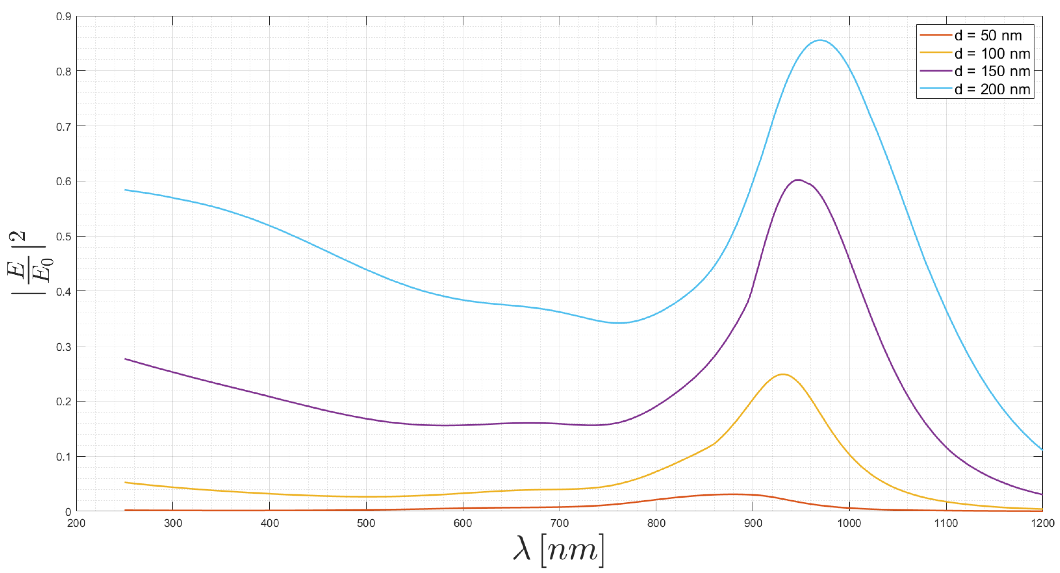
4.3. Nanoantenna Thickness Sweep
The nanoantenna thickness sweep results are respectively presented in
Figure 7 and
Figure 8, for the gold and the aluminum nanoantenna. Here, it is very important to remember that the nanoantenna is inside the dielectric medium. This one has a thickness of
and so that, when the nanoantenna thickness is varying, it is also varying the air medium thickness. This is an important statement, because all the conclusions that can be drawn will continue to be based on the assumption that the distance between the port, where the electromagnetic wave is generated, and the nanoantenna rear, which is in contact with the substrate, remains constant.
Analyzing the values for , and , it is possible to conclude that the thicker the nanoantenna is, the lower the intensity values. In addition to it, the aluminum response seems to be flatter as the nanoantenna becomes thicker.
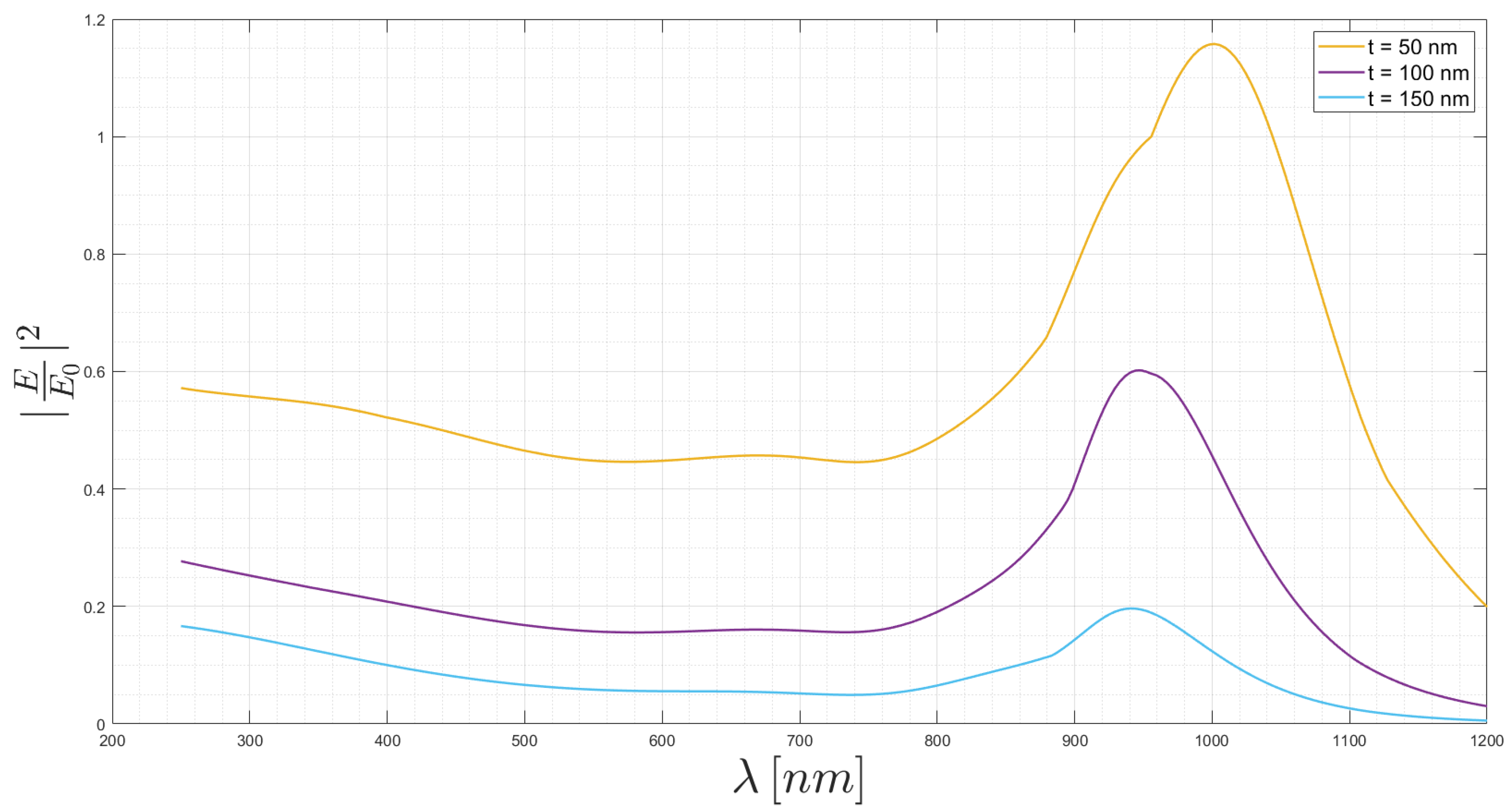
4.4. Substrate Thickness Sweep
The last sweep analyzed in this article is the substrate thickness. It is expected that as the substrate becomes thicker, the dispersion losses will be higher and, consequently, the field intensity will diminish. Based on
Figure 9 and
Figure 10, it is possible to verify it, respectively for the gold and aluminum structures. However, if the substrate becomes too thin, the generation and propagation of the surface plasmon polaritons is compromised and, consequently, the electric field is going to be weaker than expected, as verified in
Figure 9, where the gold response for
reveals a smaller intensity peak in comparison with its response for
and
.
5. Sensors
Based on the appraisal done in the previous section, a structure is defined in order to develop a sensor. A sensor is a device which, when exposed to physical or chemical phenomena (for example temperature, force, displacement, chemical elements concentration or chemical reaction), produces a proportional output signal (for example optical, electrical, mechanical or thermal) [
41,
42,
43]. However, it is called a sensor because the sensor’s input is an optical signal and its output is here only to be studied as an optical signal too, due to the fact that the output is compared and referenced to the input. Nonetheless, several materials, such as the direct band-gap semiconductors, allow us to have an electrical output (voltage or current) and so that, the device can be named as a transducer, thanks to its capability to generate a different output signal type in relation to the input one.
The intention is to create two different structures. The first one, based on the gold nanoantenna, having a gain peak on the infrared region (near ). The second, based on the aluminium nanoantenna, the planning involved the design of a sensor with a gain curve as flat as possible along all the visible region.
Based on the previous simulations, we simulated a gold structure defined by a periodicity of and a hole diameter of , which is 40% of the periodicity, as the relation between and . Moreover, the nanoantenna will have a thickness of and the substrate a thickness of . Priors tests were done in order to choose the substrate thickness. It is well-known that when the thickness decreases, the maximum gain increases. However, on the previous tests the substrate described by presents a lower peak than for . Thus, after testing both combinations of the new nanostructure, the better one with is used.
On
Figure 11, the simulation result for the defined parameter combination, clearly presents a smaller gain than some of the previously simulated structures, see for example,
Figure 9. Thus, the conclusion is that the result of the simultaneous variation of several parameters is not the sum of the results, corresponding to the variation of only one parameter at a time, the variations are not independent. As an example, if the hole diameter does not scale according to the relative periodicity percentage, the hole would be greater than the periodicity and an impossible structure results. However, all the previous rules remain, i.e., sweeping only one parameter having a reference structure will result in the same as previously mentioned. The unpredictable problem occurs when more than one parameter is swept.
Nevertheless, the gold sensors will be characterized as reported before, whose spectrum is illustrated in
Figure 11. It reached a gain of 4.67 for
, having a gain region between
and
.
The sensor with the aluminum nanoantenna guarantees gain along all of the visible region. The structure is the same as the sensor with gold. In order to create a flatter gain in the visible part of the spectrum, two other values of the nanoantenna thickness were tested. However, these results were not satisfactory, and the initial structure was chosen. The corresponding simulation results are presented in
Figure 12. In this case, the final result is better than those resulting from independently varying the different parameters of the structure one by one.
5.1. General Purposes
A sensor is characterized by a parameter whose values change with the occurrence of something. The parameter change has to be measured. Nonetheless, simpler applications must be analyzed first in order not to break the reasoning, even though these applications are not defined as sensors. For this reason, some applications are going to be covered, using the lastly presented nanostructures and the responses. The characterization of a sensor demands the measurement of a parameter whose values change with the occurrence of something. However, in some cases, the optimization of the detector, and namely of the nanoantenna response, is enough to optimize the sensor.
An example is a nanoantenna of gold used to improve the sensibility of infrared sensors, for example on medical applications, since some infrared wavelengths have high amplification and the others have huge attenuation. Then the output of the sensor presents an improved sensitivity. Another example is the oximeter, where the sensor measures the amount of oxygen on blood. There are different types, from portable to the hospital ones. In both cases, there are LEDs emitting two distinct signals; for example, on the spectral red and blue regions. The optical spectrum of blood varies with the amount of oxygen, because cells can absorb more or less radiation according to the oxygen they transport. Thus, for example using the oximeter on fingers and analyzing the output spectrum resulting from the photodetection of the red and blue light after the radiation propagates through cells, it is possible to determine the percentage of oxygen. In this case, nanoantennas can detect and amplify the detected radiation, in the two spectra intervals of interest, replacing photodetectors and increasing the device sensibility. In this case, it is suggested that a gold nanoantenna can be used to detect the red signals and a silver one to detect the blues. The overall sensibility will increase, weak signals can be generated and detected and small devices can be built.
The optical response of the nanostructure with a nanoantenna of gold can be used to improve LED and LASER sensibilities, used for example in optical communications, in a certain wavelength band. As seen in the previous simulations, changing the material of the nanoantenna, it is possible to place the peak along the frequency/wavelength range. In the case of the spectrum in
Figure 11, a near-infrared region is amplified, especially around
. Another example on communication applications is the use of these nanoantennas to convert free-space energy into guided energy and vice-versa, as it is done by a regular antenna. In this case, in addition to this conversion, the structure can be tuned to filter and amplify, using just one miniaturized device.
Lastly, the aluminum nanostructure, whose spectrum is in
Figure 12, can be used to amplify the visible and ultraviolet regions. An example of this application is on the concentration and amplification of the solar irradiance, which is predominant on the visible region, incident on the active area of a solar cell, resulting in more incident power and consequently, on more generation of output power. However, it is necessary to guarantee the chemical stability of aluminum for long-term applications.
5.2. Temperature Sensor
The first sensor, in the strict sense of the definition, is the temperature one, i.e., a thermometer. To simulate this sensor, it is necessary to have experimental results or models for the dependence of the optical properties with the temperature.
It was impossible to find air and quartz models for different temperatures. However, as these materials do not have an interband region in the simulated range, it is not necessary to have its models. On the other hand, the temperature has a small influence on the dielectric function real part, in comparison with the imaginary one. Thus, the influence of the metal will always be predominant and so therefore, structures as the ones presented in this work can be used as temperature sensors [
21,
22,
23].
A temperature sensor based on a gold nanoantenna is going to be simulated, for five different temperatures, T (
,
,
,
and
), using models for each temperature [
44]. The real part of the gold dielectric function is almost independent of the temperature until approximately a wavelength of
[
44]. After it, the temperature dependence can be divided into two different groups. First, for each wavelength, as the temperature increase, the real part of the dielectric function becomes smaller [
44]. However, there is a specific temperature value, the critical temperature value(s), where an inversion of this rule starts. In this case, between
and
, the real part of the dielectric function becomes abruptly higher than the values for smaller temperatures [
44]. After that, the higher the temperature is, the higher the real part of the dielectric function will be [
44]. On the other hand, the imaginary part seems to have a temperature dependency along all of the simulated range however, only above approximately a wavelength of
a strict rule seems to be established [
44]. Below it, the dependency is not well defined. However, the model analysis is not the most important because the output optical response has yet to be verified, and this is the spectral response that will allow us to conclude about the sensor design.
In this case, and for this range of temperatures, there is only one of these temperature values, known as the critical temperature, which is between
and
. Thus, it is possible to study this sensor in two different work regions: the first where the peak value increases with the temperature and the second where this value decreases as the temperature increases. In the
Figure 13 and
Figure 14 are illustrated the nanostructure behavior, both for temperatures below the critical one and for temperatures above the critical one.
There, it is observable that it is possible to differentiate each temperature only using the maximum gain value. Moreover, as expected, the conclusions taken from the complex dielectric function analysis are reflected on the nanostructure response.
Furthermore, based on
Figure 15, which is the combination of the responses shown in
Figure 13 and
Figure 14, it is quite impressive how the spectrum retains the same shape and intensity values, in spite of the temperature variation, except in the work region (the peak values).
These simulations allow us to conclude that each temperature will generate a different nanostructure response, which is well defined. Thus, measuring the output spectrum at wavelengths near the peak one, it is possible to determine what is the temperature around the nanostructure, since different temperatures produce different output electric field norms. The sensibilities of this specific structure (with this physical parameters) are presented in
Table 1. There, it is possible to observe that the most sensible temperature range is the one above the critical value, in terms of gain variation. On the other hand, it is important to remember that this structure is not able to associate wavelength shifts to temperature variations, since its sensibility has a small value.
This structure is not optimized to have the highest sensitivity. Nonetheless, the aim of this article is accomplished since it is shown that this structure can be tuned and work as a sensor. Better sensibilities can be found using an application for multi-factorial optimization.
Moreover, if the critical temperature of gold is available, the determination of the temperature value only demands the measurement of the output signal for a given wavelength of the input signal. If the peak value and the uncertainty range are specified for each structure, it is possible to use only one wavelength measurement, since around the peak there are no equal values for different temperatures.
Finally, the last conclusion that has to be clearly explained is the possibility of producing electrical energy. First, at around room temperature the nanostructure has optical gain; however, after a certain temperature, the gain will increase as the temperature increases. For that reason, it is possible to tune the energy production and actually generate energy using, for example, chemical reactions to produce heat and the environment radiation, which is the opposite of having the nanoantenna as a temperature sensor for chemical reactions.
5.3. Tissues Detection Sensor
The sensor should detect different tissues from their optical properties. In the considered range of wavelengths, the sensor is tested by analyzing the response to four types of biological tissues (liver tissues, colon mucosa tissues, colon submucosa tissues and colon serosa tissues) and the main goal was to use the gold and the aluminum nanostructures in order to detect the tissue over the nanoantenna [
40]. As illustrated in
Figure 16, the sensor structure is similar to those previously considered. However, the tissues are placed between the dielectric and the nanoantenna. Thus, the nanoantenna holes will be covered by those tissues instead of the dielectric. The tissue medium has a thickness of
, but only
is visible in the figure since the remainder is the nanoantenna thickness. The dielectric has also a thickness of
.
Due to the model’s wavelength range, the following simulations were done between and .
First, the gold made nanostructure is simulated considering the aforementioned tissues and its results are presented in
Figure 17, where it is possible to verify that all the tissues responses are similar. It is noticeable that different tissues will produce different spectral peaks. In this case, it is possible to distinguish liver and three types of colon tissues. As expected, the difference among colon tissues is smaller than the difference between any colon tissue and the liver one.
However, analyzing the spectral region near the peak, it is possible to better observe that even the colon tissues can be differentiated, as illustrated in
Figure 18, with different wavelengths.
The spectral variation values are presented In
Table 2 and
Table 3, respectively for the peak and peak wavelength. There, it is possible to observe that the liver is easier to distinguish from any colon tissue, than the distinction among colon tissues.
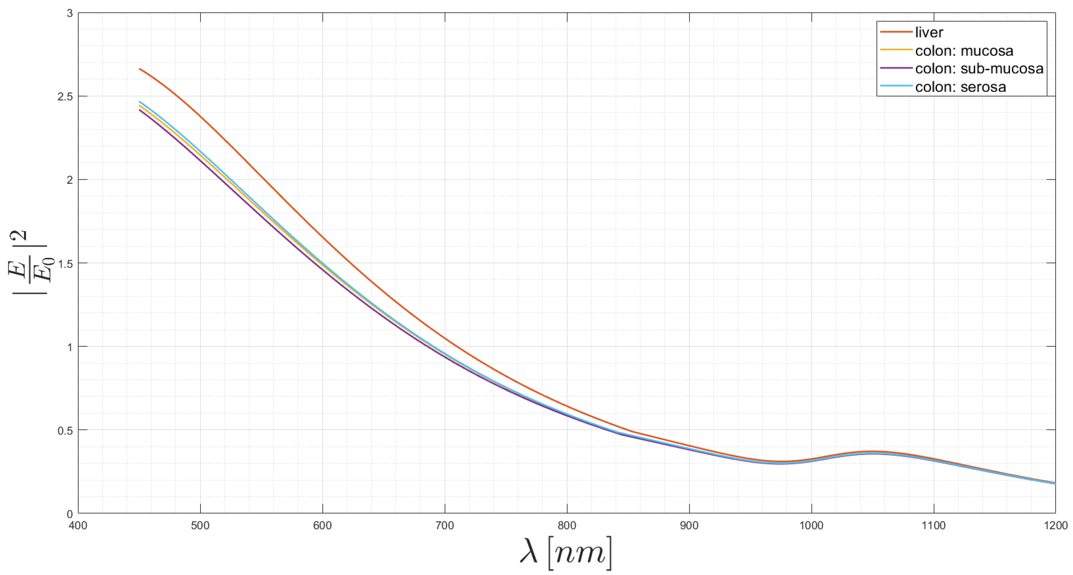
The same simulations were done using the aluminum nanoantenna, whose results are presented In
Figure 19. There, although all the responses are very similar at higher wavelengths, the region around
, that is in focus in
Figure 20, allows the detection of each tissue. Once again, the liver can be easily differentiated from the colon cells; however, it can be possible to distinguish similar tissues, as the colon ones.
As predictable from the parameters’ study, the aluminum optical response does not have a well-defined peak for this range. Thus, it is not possible to analyze the variation of the wavelength peak. Therefore, in
Table 4 and
Table 5, we present respectively the gain variation for 500 nm and for 700 nm. Based on these tables, it is possible to verify that the structure is more sensible for wavelengths near 500 nm than for wavelengths around 700 nm. Once again, it is observed that the distinction of liver from the colon tissues is easier to detect than to differentiate cells only from colon tissues.
One way to distinguish more similar characteristics is to do this analysis along the whole spectrum, because there are more than one single region where the tissues lead to different response values. Nonetheless, based on which tissues are being distinguished, it can be possible to use just one single wavelength. For example, to distinguish liver from one of the colon samples, it is possible to use just one wavelength; however, to distinguish similar tissues, as the colon ones, it is much better to analyze the whole range. Furthermore, considering a group of structures (with different materials, parameters and typologies), it is possible to increase the method reliability by comparing the obtained responses to the same input.
In addition, it can be possible to create a huge database of optical responses like these for each tissue. Some of them should be unhealthy tissues, for example cancer cells at different stages or cells affected by diseases such as diabetes [
45]. Thus, there are already some studies that report how the diseases affect the optical properties of biological tissues [
45]. Then, the spectral response will vary and it is possible to monitor cells and tissues in real time, in vitro or in vivo, in order to create a regular report of spectra like these [
10,
24,
25,
27]. It is useful to detect some diseases or to control substance levels [
10,
21,
24,
25,
26,
46,
47]. For instance, if optical properties vary with the concentration of some substances, it is possible to take conclusions regarding the spectral analysis. It is the case for insulin levels (diabetes), blood pressure or oxygen in circulation. Nonetheless, it is very important to have a huge database, in order to create a complex dielectric function model to use on these applications. These real models are not easily available.
6. Conclusions
The discovery of the extraordinary optical transmission questioned all the classical theories of diffraction of the electromagnetic field. None of them explain the new phenomenology, because it is assumed the existence of ideal materials, namely metals. In doing so, the generation and propagation of surface plasmon polaritons and of creeping or leaky waves is not considered and, consequently, the classical theories fail. The consideration of these effects demand the consideration of the electrical and optical properties of real materials, through a correct modeling of the dielectric function and refractive index. Then, the propagation of surface plasmon polaritons can be theoretically analyzed from Maxwell’s equations. Their generation and propagation, combined with the propagation of creeping waves, especially out of the visible spectral region, allow to describe the extraordinary optical transmission phenomenon. Moreover, if the nanoantenna is not metal made or if the incident field has a frequency away from the visible region, other wave phenomena (for example, the propagation of creeping and leaky waves) become more important than the polaritons ones, that may not even be generated, although EOT can occur.
Thus, EOT can be observed using metallic nanoantennas. This kind of structure allows the concentration and amplification of electromagnetic energy. Using a Finite Element Tool, it was created a 3D simulation environment to model and simulate a metallic nanoantenna, obtaining its optical response at frequencies on the visible and near-infrared regions. The optical response is dependent on the used materials, on the nanoantenna and also on the surrounding materials.
Furthermore, it is possible to verify that for the gold nanostructure, when the structure periodicity increases, the maximum intensity value decreases, keeping the same peak wavelength value. On the aluminum spectra, it is concluded the periodicity affects the flatter region, the region that can have gain. In relation to the hole diameter sweep, it is possible to verify that the larger the hole is, the higher the intensity peak is. However, in this case, a careful conclusion should be drawn, because it is also known that the hole diameter should be much smaller than the incident wavelength. In addition to this effect, red shifts will occur as the diameter increases. The nanoantenna thickness is also analyzed. Considering the previous simulations, it is possible to conclude that the thicker the nanoantenna is, the less the peak intensity will be. In addition, blue shifts will occur in this situation and, specifically on the aluminum response, it seems that the flat region becomes flatter. The substrate thickness leads to the idea of adjusting losses and consequently gains without changing the spectrum shape. The thicker the substrate is, the higher the losses are, keeping the optical response shape.
The simulations’ results also lead to the conclusion that the spectral response can be tuned by varying the topology and the parameters of the structure. However, in order to create rigorous analytical models, a huge simulation database has to be created, requiring huge computational efforts. Furthermore, all the simulations show high amplification and concentration of the electromagnetic field near the interfaces. This is a clear evidence of the generation and propagation of surface plasmon polaritons.
The nanostructure of gold was simulated as a temperature sensor, using models for the complex dielectric function including the temperature. A nanostructure like this can behave as a temperature sensor with a critical temperature. Below this critical value, the peak of the optical response decreases with the increase of temperature, but the corresponding wavelength remains almost constant. Above the critical value, the peak of the optical response increases with temperature and the peak wavelength is slightly shifted to a greater wavelength.
A sensor to distinguish human body tissues was also simulated using the gold and the aluminum nanostructure. The simulated structures can distinguish different tissues and even detect diseases. However, to detect diseases, it is very important to have a huge database in order to create models of the electrical permittivity (complex dielectric function), of healthy and unhealthy tissues. The creation of good models for the different structures, and the creation of new structures, used to distinguish the human tissues and detect the diseases, is also very important.
To sum it up, some structures based on the occurrence of extraordinary optical transmission were modeled and simulated. Several simulations were presented to discuss the influence of the materials and of the geometrical parameters on the optical response of the structures. The obtained results clearly point to the development of the project of miniaturized sensors, that could be used to detect and measure temperature variations, to distinguish different human tissues and, consequently, in some cases to detect diseases.


