Abstract
The development of electronic devices with enhanced properties of transparency and conformability is of high interest for the development of novel applications in the field of bioelectronics and biomedical sensing. Here, a fabrication process for all organic Organic Field-Effect Transistors (OFETs) by means of large-area, cost-effective techniques such as inkjet printing and chemical vapor deposition is reported. The fabricated device can operate at low voltages (as high as 4 V) with ideal electronic characteristics, including low threshold voltage, relatively high mobility and low subthreshold voltages. The employment of organic materials such as Parylene C, PEDOT:PSS and 6,13-Bis(triisopropylsilylethynyl)pentacene (TIPS pentacene) helps to obtain highly transparent transistors, with a relative transmittance exceeding 80%. Interestingly enough, the proposed process can be reliably employed for OFET fabrication over different kind of substrates, ranging from transparent, flexible but relatively thick polyethylene terephthalate (PET) substrates to transparent, 700-nm-thick, compliant Parylene C films. OFETs fabricated on such sub-micrometrical substrates maintain their functionality after being transferred onto complex surfaces, such as human skin and wearable items. To this aim, the electrical and electromechanical stability of proposed devices will be discussed.
1. Introduction
Flexible organic electronics are considered a valuable technology for the development of innovative devices that can be complementary to those based on standard electronic processes. Indeed, overturning the standard paradigm of electronics, this peculiar technology emphasizes peculiar properties, such as flexibility and transparency, and the possibility of cost-effective fabrication over large areas. All these features are of great importance for the future exploitation of flexible organic electronic devices in real products for electronic, optoelectronic and bioengineering applications: optical transparency is fundamental in different biochemical applications [1,2,3], and extreme flexibility is needed for the development of imperceptible, wearable and even tattoo-like devices [4,5,6,7,8,9,10,11]. In this scenario, the possibility of up-scaling device fabrication to an industrial size is not secondary, in order to ensure future market exploitation, as well as low-voltage operation for actual portability and user safety.
Among flexible organic devices, Organic Field-Effect Transistors (OFETs) are surely of great interest, as they can employed both as basic building blocks in electronic circuits [12,13,14] and as sensors [15,16,17]. In the bioelectronic scenario, peculiar optical and mechanical properties must be combined with low-voltage operation of the devices, in order to ensure portability and user safety. Although significant steps forward have been reported by the recent literature, the actual combination of low-voltage operation, transparency, flexibility and large-area fabrication processes is substantially missing. Indeed, several examples of transparent OFETs may be found in the literature [18,19,20,21,22] with moderately or even high operating voltages and fabricated over rigid substates, as well as low-voltage and transparent devices which are not flexible [23,24]. When flexibility and transparency are combined, moderately high voltages are reached or small-area fabrication processes are involved [25,26,27,28,29,30]. This is mainly related to the fact that low-voltage operation is generally reach by ensuring large gate insulator capacitance; this can be obtained by using high-k dielectrics [31] or reducing the gate insulator thickness. High-k materials, such as inorganic dielectrics, can be transparent and reasonably flexible, but normally requires high process temperatures, and are thus not suitable for the employment of most of the plastic substrates. Organic dielectrics can be processed at room temperature and by liquid phase, but low-voltage operation is allowed by depositing them in very thin films, as their dielectric constant is relatively low. Unfortunately, obtaining such thin films (generally in the range of a few tens of nanometers) is not trivial with large-area processes, and only a couple of examples have been reported so far in the literature. As a matter of fact, only a few examples combining low voltage operation, transparency and flexibility are available to date [32,33], but small-area techniques, such as spin-coating, still cover a central role in the fabrication process, e.g., for the deposition of a gate insulator layer thin enough to ensure low-voltage operation.
In this paper, transparent, all-organic, low-voltage OFETs over a fully flexible substrate will be reported. The fabrication process here presented employs only large-area techniques, namely ink-jet printing and Chemical Vapor Deposition (CVD), that can be easily up-scaled to an industrial size. As CVD allows the uniform deposition of very thin dielectric layers at room temperature, such a fabrication process can skip the limitations of solution-processed dielectrics, and can be adapted to different kind of substrates, from flexible—but relatively thick—plastics to ultra-conformable, tattoo-like (thickness < 1 μm) ones. Therefore, flexibility can be brought to the very far end, towards the fabrication of devices that can conform to every surface, even to the human skin for epidermal electronics applications. The reliability of the fabrication process and reproducibility of electrical performances will be discussed over a statistically relevant number of devices on both kinds of substrates. A quantification of the overall device transparency will be provided. A bias stress test will be reported in order to demonstrate significant electrical stability of fabricated OFETs. The complete functionality of ultra-conformable OFETs on skin will be reported, as well as a clear demonstration of the mechanical and electrical stability of free-standing devices over different bending degrees.
2. Materials and Methods
2.1. Device Structure and Fabrication
Fabricated OFETs have a bottom gate-bottom contact structure, shown in Figure 1. Two different substrates were employed: 175-μm-thick polyethylene terephthalate (PET, Goodfellow) and 700-nm-thick Parylene C substrates. The latest were fabricated by depositing Parylene C with a PDS 2010 Labcoater 2 (Specialty Coating System, Indianapolis, IN) over 175-μm-thick PET substrates, previously coated with 1:50 water solution of an industrial soap (Micro-90 Concentrated Cleaning Solution, International Corporation, Burlington, NJ). Before printing, both kinds of substrate were cleaned with acetone and ethanol (Sigma Aldrich) and dried with nitrogen. Gate electrodes were inkjet-printed using a Dimatix Materials Printer DMP2831 (Fujifilm Dimatix, Lebanon, NH). A 16-nozzle cartridge with single drop volume of 1 pL (DMC11601, Fujifilm Dimatix) was filled with PJET HC (Heraeus, Hanau, Germany), a commercially available, Poly(3,4-ethylenedioxythiophene)-poly(styrenesulfonate) (PEDOT:PSS)-based ink. Three nozzles, biased with a firing voltage of 25 V, were employed for patterning gate lines of 10 × 2 mm2, defined by the overlap of two subsequently printed layers. A drop spacing of 20 μm was set, and the printer platen was maintained at a fixed temperature of 60 °C. The gate insulator is a 250 nm-thick Parylene C film, deposited by CVD using the previously cited PDS 2010 Parylene coating equipment. In this case, an adhesion promoter (A-174 Silane, Specialty Coating Systems, Indianapolis, IN) was inserted in the deposition chamber to improve the quality of the deposited film. It is worth noting that this technique is perfectly compatible, in terms of throughput and area, with inkjet printing [34,35], and can be possibly extended to roll-to-roll fabrication processes [36]. The final insulating capacitance is of 10 nFcm−2.
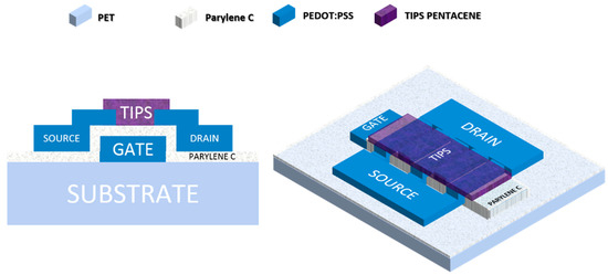
Figure 1.
Section and 3D cartoon showing the Organic Field-Effect Transistor (OFET) structure and employed materials.
After a thorough cleaning of Parylene C surface with acetone and ethanol, the source and drain electrodes were inkjet-printed using PJET HC, in the same conditions described for gate patterning (with the exception of the employment of a single nozzle). Interdigitated structures comprising 10 channels were fabricated by printing 2-mm-long, 200-μm-wide and 175-μm-spaced electrodes. A final channel width W = 20 mm and channel length L = 100 μm were obtained. Source and drain electrodes were post-processed with a curing step over a hot plate (90 °C for 15 min) and a subsequent deposition of ethylene glycol (EG, Sigma Aldrich) by inkjet printing, using a cartridge with a single drop volume of 10 pL (DMC11610, Fujifilm Dimatix), two nozzles with a firing voltage of 40 V and a drop spacing of 80 μm. EG was left to dry for 30 min over the printer platen at a temperature of 60 °C. 6,13-Bis(triisopropylsilylethynyl)pentacene (TIPS pentacene, Sigma Aldrich) was printed from a 1.5 wt % solution in anisole (Sigma-Aldrich), using a cartridge with a single drop volume of 10 pL, employing three nozzles biased at 40 V, with a drop spacing of 30 μm, and leaving the platen at room temperature. This semiconductor was chosen for its significant air stability [37] and its moderately high charge carrier mobility [38]. Figure S1 in Supplementary Information shows the obtained device structure, and some details obtained using the fiducial camera of the printer.
2.2. Electrical and Electromechanical Characterizations
All characterizations were carried out in ambient conditions, using a Keithley SourceMeter® 2614, controlled with custom-made Matlab® softwares. Ultra-thin devices were characterized by gently gluing conductive wire on connection pads by means of silver paste. Bias stress tests were carried out by means of an Agilent B1500A Semiconductor Parameter Analyzer. Electromechanical characterization was performed using graduated cylinders for the largest values, and common objects (doctor blades, conductive wires) to evaluate the extreme bendability of devices. Current characteristics were acquired by means of an Agilent B1500A Semiconductor Parameter Analyzer.
2.3. Optical Characterization
Absorption characterization was performed in air with the Perkin Elmer double beam LAMBDA 1050 UV/Vis Spectrophotometer.
3. Results
3.1. Electrical Characterization
Figure 2 reports the typical output and transfer characteristic curves of the fabricated device on the different kinds of substrate mentioned in the Materials and Methods section. Polyethylene terephthalate (PET) has been considered for its high transparency as a conventional substrate for initial process setup and optimization. A standard thickness of 175 μm was considered, thus giving a significant flexibility to fabricated devices. A total number of 50 OFETs were fabricated and tested in five different batches, with a process reliability of 98% (one device in 50 short-circuited). Typical output and transfer characteristic curves are reported in Figure 2a,b, respectively. Devices can operate at gate-to-source (VGS) and drain-to-source (VDS) not exceeding 3 V in absolute value, with a threshold voltage around 0 V. From the output characteristic curves, it is possible to observe that a good current stability in saturation regime has been obtained, as well as a significant field-effect current modulation. From the linear regime, no significant contact resistance effects can be observed. These elements suggest that ideal charge carrier injection conditions have been obtained, as well as the ideal insulator–semiconductor interface. This is also confirmed by the negligible hysteresis that can be observed from transfer characteristic curves, both in linear and saturation regime. Interestingly enough, the gate-to-source current (IGS, from now on leakage current) is in the range of 10−10 A, thus demonstrating that a very good insulation of the gate electrode was obtained with a Parylene C layer thin enough (around 250 nm) to ensure the capacitance per unit are suitable for low-voltage operation. The sub-threshold current, which mainly depends on leakage current, is therefore in the same order of magnitude; this could be further reduced by decreasing the gate dielectric thickness in order to enhance gate coupling, but this may affect the process reliability and leakage current. Nonetheless, an on/off current ratio of 104 is obtained, although a limited aspect ratio was designed. The assessed fabrication process was then transferred onto ultra-conformable, 700-nm-thick Parylene C substrates, thus obtaining the thinnest, all-organic transparent OFET reported in the literature to the best of our knowledge. According to the procedure described in Lai et al., [11] Parylene C was deposited over 175-μm-thick PET carrier substrates, previously coated with a soap solution. The amphoteric molecules of the soap reduce the adhesion of Parylene C to substrates, thus making its mechanical peel-off possible in dry conditions after the fabrication process is completed. This property made the transfer of the substrate from the carrier substrate to the final support easier than wet peel-off and recovery from the surface of the liquid, and also ensured the absence of solvent residues. Thirty devices were fabricated in this configuration on two different batches; in this case, only two devices (one per batch) were not functioning, thus maintaining the reliability of the process at above 93%. Representative characteristic curves, shown in Figure 2c,d, show that the overall electrical characteristics are comparable to those obtained over standard PET substrates. A slightly larger (but still negligible) hysteresis is noticeable; it is also qualitatively evident that mobility is slightly lower than those obtained on PET, as channel conductance (the slope of the linear regime in output characteristic curves) is lower. These results may be justified by the larger roughness of the Parylene C substrate, due to the non-perfect uniformity of the amphoteric molecule layer deposited on the carrier substrate.
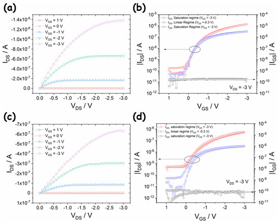
Figure 2.
Typical output (a) and transfer characteristic curves (b) of OFETs fabricated over 175 μm-thick PET substrates; typical output (c) and transfer characteristic curves (d) of OFETs fabricated over 700 nm-thick Parylene C substrates.
In order to statistically characterize the electrical performance of fabricated devices on PET and ultra-thin Parylene C films, basic electrical parameters were extrapolated by transfer characteristic curves; average and 1-σ confidence band values for these parameters are reported in Table 1. Devices fabricated on both PET and Parylene C substrates are in enhancement mode, with a negative threshold voltage in the range of 0 V (−0.1 ± 0.16 V on PET, 0 ± 0.1 V on Parylene C). On PET, an average charge carrier mobility of 0.25 cm2V−1s−1 was obtained, which is a remarkable value for a non-purified TIPS pentacene solution deposited by inkjet printing. The subthreshold slope is about 130 mVdec−1, a significant value for low-voltage OFETs, demonstrating one more time that the insulator/semiconductor interface is almost ideal. Indeed, this parameter is related to the maximum surface trap concentration by the well-known relationship [39]
where CINS is the capacitance per area unit of the insulator, q the elementary charge, SS the subthreshold slope, and T the absolute temperature. Using this equation, a maximum surface trap states concentration of 1.3 × 1011 cm−2 eV−1 can be obtained, which is comparable to or lower than the ones for low-voltage structures with a much higher gate capacitance. As previously discussed, a slight reduction in charge carrier mobility was observed on ultra-thin substrates (0.13 ± 0.04 cm2 V−1 s−1); at the same time, a slight increase in subthreshold slope (i.e., an increase of NSSmax) was recorded, as a further demonstration of a sensible worsening of the insulator/semiconductor interface. It is worth noting that these values remain valuable for a low-voltage, all-organic device. For both structures, the average leakage current is in the range of 100 pA.

Table 1.
Average and 1-σ confidence band for the basic electrical parameters of OFETs fabricated on PET (evaluated on 50 devices) and Parylene C substrates (evaluated on 30 devices).
3.2. Electrical Stability
The stability of electrical parameters upon continuous bias is fundamental for the development of any user application. Figure 3 reports a bias stress test consisting of a continuous acquisition of 1000 transfer characteristic curves, in double-sweep mode and in ambient conditions. From Figure 3a, it is possible to notice that measurements are almost perfectly overlapped, thus demonstrating a good stability of electrical performances during the whole experiment. To better characterize the electrical stability of the proposed devices, threshold voltage and mobility were extracted from transfer characteristic curves; results are reported in Figure 3b. It is possible to notice that the threshold voltage almost linearly increased, passing from −180 to −30 mV, with a shift not exceeding 150 mV upon several hours of continuous operation. Charge carrier mobility remained almost stable for the 200 cycles, then started to decrease, passing from 1.1 to 1 × 10⁻² cm2V−1s−1, with a relative reduction of about 10%. Such results are consistent with what is already demonstrated in the literature for TIPS pentacene [37].
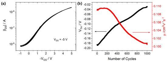
Figure 3.
(a) 1000 double-sweep transfer characteristic curves acquired in saturation regime at VDS = −5 V; (b) threshold voltage (black, left axis) and mobility (red, right axis) absolute variations extrapolated by the square root of curves in (a).
3.3. Electromechanical Characterization
Taking advantage of the conformability of the ultra-thin Parylene substrates, the fabricated OFETs can be employed in tattoo electronics applications.
The first fundamental property for a tattoo electronic element is the mechanical stability. Indeed, thanks to their ultralow thickness, Parylene substrates conformably adhere to micrometric “ridged” features of epidermal crests, thus possibly being subjected to significant surface strain values. The surface strain has the effect of modifying the morphology of the organic semiconductor layer [40,41], thus determining a variation in the electrical properties of the device, in particular the charge carrier mobility. Surface strain is directly proportional to device thickness, according to the relationship
where tsub and td are substrate and device thickness, respectively, η = td/tsub and χ = Yd/Ysub, being Yd and Ysub the Young’s moduli of device and substrate, respectively, and R is the bending radius. It is noteworthy that, as strain is directly proportional to the overall device thickness (tsub + td), the strain produced by a certain deformation on a sub-micrometrical OFET can be very low even for low values of R. In order to demonstrate that device performances are substantially stable with bending, ultra-thin OFETs have been bent at different bending radii (R = 3.5, 3, 2.5, 1.5, 1, 0.8, 0.5, 0.1 cm), both in extension and in compression. In extension, a tensile strain is applied on the organic semiconductor, and this would bring a reduction in charge carrier mobility due to the displacement of crystalline domains in the film. On the contrary, when the device is compressed, the local density of crystalline domains in the organic semiconductor film increases, thus bringing an increase in the charge carrier mobility. Results are reported in Figure 4: in Figure 4a, relative charge carrier mobility variations with the applied bending radii are reported, calculated as (μb − μf)/μf (μb and μf are charge carrier mobility values in bent and flat conditions, respectively). In both extension and compression, average fluctuations of mobility values in the range of 2% were recorded, without any evident trend with applied deformation in both cases, thus demonstrating that complete mechanical stability has been obtained. This is consistent with the fact that, although the significant deformation applied, the surface strain applied in both cases is very low (as high as 0.05%) as the whole device thickness is much lower than the applied deformation. The overall stability of devices can also be demonstrated for an extreme deformation, obtained by bending the device over a copper wire with a nominal diameter of 150 μm. A plot showing the actual transfer characteristic curves of a device in flat conditions (black solid squares) and during bending (black open squares) is reported in Figure 4b. Curves are almost completely overlapped, with a minimum shift in the threshold voltage and OFF current increase, which can be ascribed to the measurement setup (devices are connected to quite long conductive wires in order to allow such an extreme deformation). These results further demonstrate the complete mechanical stability of the device.
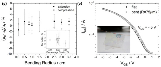
Figure 4.
(a) Percentage charge carrier mobility variation as a function of mechanical deformations at different bending radii (R = 3.5, 3, 2.5, 1.5, 1, 0.8, 0.5, 0.1 cm) in extension (solid squares) and compression (open squares). In the inset, the corresponding surface strain is shown (extension for positive values, compression for negative values). (b) Transfer characteristic curves of an ultra-conformable OFET in flat conditions (solid squares) and while bent over a copper wire with a diameter of 100 μm (open squares, see picture in the inset).
3.4. Optical Characterization
Thanks to the appropriate choice of materials, fabricated OFETs are significantly transparent. In order to quantify the actual transparency, absorbance tests have been carried out in the visible spectra (400–800 nm). Results are summarized in Figure 5, where transmittance is reported for complete devices fabricated both on PET and Parylene ultra-thin films. Devices have four well=defined absorption peaks (490, 600, 650 and 700 nm, see Figure S3 in Supporting Information), which are consistent with those typically reported for TIPS pentacene in different kind of solvents [42,43,44]. At these wavelengths, the transmittance is of about 70% for devices fabricated on PET, and of about 75% on Parylene C. It is worth noting that the transmittance of the transistor structure fabricated on PET before the semiconductor deposition exceeds 80%; if this data is compared with the transmittance of bare PET (85%), a relative transmittance of 94% can be derived for devices fabricated on PET without a semiconductor, which is reduced to 82% due to TIPS pentacene absorbance. Therefore, the actual transparency can be further improved by properly choosing a material more transparent than TIPS pentacene as the active layer.
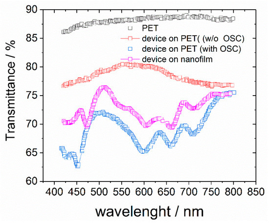
Figure 5.
Transmittance for bare PET (black), OFETs fabricated on PET without (red) and with (blue) TIPS pentacene, and for ultra-conformable devices on Parylene C films (magenta).
3.5. Proof-Of-Concept Application to Transparent Tattoo Electronics
Thanks to the reliability of the fabrication process over different kinds of flexible substrates, the electromechanical stability of ultra-conformable OFETs and the significant transparency, the proposed device structure and fabrication process is a valuable candidate for the development of several applications, such as those of wearable electronics and bio-electronics.
Tattoo electronics represent the final frontier for flexible wearable electronics, as it aims towards transferring complex device functionality on the skin of the user. To this aim, ultra-conformability and mechanical stability are fundamental features for every tattoo-like device. In order to demonstrate the suitability of the proposed technology for tattoo electronics, OFETs fabricated on ultra-thin films where transferred and characterized on the skin; Figure S2 shows an example of an OFET successfully transferred onto a finger. As previously demonstrated by Lai et al. [11], an ultra-thin Parylene C film with mechanical features identical to those employed in this paper can perfectly adhere to the ridged structures of the skin, and is thus ideal for the development of epidermal electronic applications. As shown by Figure 6, typical output and transfer characteristic curves for a device operating on skin substantially maintain the same electrical features as free-standing transistors, with a slight shift in the threshold voltage towards more negative values and an increase in the leakage current to a few nA. The combination of significant mechanical stability, conformability to human skin and high transparency make the proposed devices of wide interest for the development of tattoo-like applications with enhanced properties of imperceptiveness and comfort to users. Their application in epidermal circuits and biochemical sensors is being currently explored and will represent a follow-up of this proof-of-concept demonstration of actual device functionality on skin.
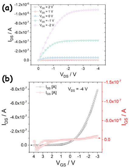
Figure 6.
Output (a) and transfer characteristic curve (b) of an ultra-conformable OFET transferred onto the skin.
4. Conclusions
In this paper, a novel, transparent, all-organic OFET structure has been presented. With respect to other devices reported in the literature, the low voltage operation and the sole employment of large-area fabrication techniques, namely inkjet printing and chemical vapor deposition, can be highlighted. Interestingly enough, the same fabrication process can be applied to different kinds of substrates, from flexible PET to ultra-thin, compliant Parylene C films. A statistical characterization of the devices’ performance on both kinds of substrates demonstrates that these devices can be operated at voltages not exceeding 3 V (on PET) and 4 V (on Parylene C), with significant reproducible electrical parameters: the threshold voltage is close to 0 V, the charge carrier mobility exceeds 0.1 cm2V−1s−1 and the subthreshold slope is in the range of 100 mVdec−1. Ultra-thin devices, with a relative transmittance exceeding 80%, maintain their functionalities when transferred onto different surfaces, including human skin, where a significant conformability to its ridged structures has been demonstrated. Good electrical and electromechanical stability has been demonstrated, with restrained threshold voltage and mobility variations upon 1000 bias cycles and negligible mobility degradation at significant deformations. The unique characteristics of transparency and conformability reported here pave the way for the development of innovative devices for epidermal electronics and wearable sensor applications.
Supplementary Materials
The following are available online at https://www.mdpi.com/2076-3417/10/19/6656/s1. Figure S1: pictures showing fabricated devices with highlighted gate, source and drain structures, and microphotographs obtained during source/drain printing process with the fiducial camera of the printer. Figure S2: Pictures showing the successful transfer of ultra-conformable OFETs to human skin. Figure S3: Absorbance for bare PET (black), OFETs fabricated on PET without (red) and with (blue) TIPS pentacene, and for ultra-conformable devices on Parylene C films (magenta). These data correspond with those on transmittance reported in Figure 5 of main paper.
Author Contributions
S.L. and G.C. designed and fabricated devices. S.L. and G.C. performed electrical, electromechanical and optoelectronic testing. P.C.R. performed optical characterization. P.C. and A.B. coordinated research activities. All authors equally contributed to the analysis of the results and writing of the paper. All authors have read and agreed to the published version of the manuscript.
Funding
This research received no external funding.
Conflicts of Interest
The authors declare no conflict of interest.
References
- Park, D.-W.; Schendel, A.A.; Mikael, S.; Brodnick, S.K.; Richner, T.J.; Ness, J.P.; Hayat, M.R.; Atry, F.; Frye, S.T.; Pashaie, R.; et al. Graphene-based carbon-layered electrode array technology for neural imaging and optogenetic applications. Nat. Commun. 2014, 5, 5258. [Google Scholar] [CrossRef] [PubMed]
- Williamson, A.; Ferro, M.; Leleux, P.; Ismailova, E.; Kaszas, A.; Doublet, T.; Quilichini, P.; Rivnay, J.; Rózsa, B.; Katona, G.; et al. Localized neuron stimulation with organic electrochemical transistors on delaminating depth probes. Adv. Mater. 2015, 27, 4405–4410. [Google Scholar] [CrossRef] [PubMed]
- Lee, W.; Kim, D.; Matsuhisa, N.; Nagase, M.; Sekino, M.; Malliaras, G.G.; Yokota, T.; Someya, T. Transparent, conformable, active multielectrode array using organic electrochemical transistors. Proc. Natl. Acad. Sci. USA 2017, 114, 10554–10559. [Google Scholar] [CrossRef] [PubMed]
- Gentner, R.; Classen, J. Development and evaluation of a low-cost sensor glove for assessment of human finger movements in neurophysiological settings. J. Neurosci. Methods 2009, 178, 138–147. [Google Scholar] [CrossRef]
- Fuh, Y.-K.; Ho, H.-C. Highly flexible self-powered sensors based on printed circuit board technology for human motion detection and gesture recognition. Nanotechnology 2016, 27, 095401. [Google Scholar] [CrossRef]
- DeGraff, J.; Liang, R.; Le, M.Q.; Capsal, J.-F.; Ganet, F.; Cottinet, P.-J. Printable low-cost and flexible carbon nanotube buckypaper motion sensors. Mater. Des. 2017, 133, 47–53. [Google Scholar] [CrossRef]
- Lai, S.; Garufi, A.; Madeddu, F.; Angius, G.; Bonfiglio, A.; Cosseddu, P. A Wearable Platform for Monitoring Wrist Flexion and Extension in Biomedical Applications Using Organic Transistor-Based Strain Sensors. IEEE Sens. J. 2019, 19, 6020–6028. [Google Scholar] [CrossRef]
- Huang, X.; Liu, Y.; Cheng, H.; Shin, W.; Fan, J.A.; Liu, Z.; Lu, C.; Kong, G.; Chen, K.; Patnaik, D.; et al. Materials and designs for wireless epidermal sensors of hydration and strain. Adv. Funct. Mater. 2014, 24, 3846–3854. [Google Scholar] [CrossRef]
- Kim, J.; Salvatore, G.A.; Araki, H.; Chiarelli, A.M.; Xie, Z.; Banks, A.; Sheng, X.; Liu, Y.; Lee, J.W.; Jang, K.-I.; et al. Battery-free, stretchable optoelectronic systems for wireless optical characterization of the skin. Sci. Adv. 2016, 2, e1600418. [Google Scholar] [CrossRef]
- Park, D.Y.; Joe, D.J.; Kim, D.H.; Park, H.; Han, J.H.; Jeong, C.K.; Park, H.; Park, J.G.; Joung, B.; Lee, K.J. Self-powered real-time arterial pulse monitoring using ultrathin epidermal piezoelectric sensors. Adv. Mater. 2017, 29, 1702308. [Google Scholar] [CrossRef]
- Lai, S.; Zucca, A.; Cosseddu, P.; Greco, F.; Mattoli, V.; Bonfiglio, A. Ultra-conformable Organic Field-Effect Transistors and circuits for epidermal electronic applications. Org. Electron. 2017, 46, 60–67. [Google Scholar] [CrossRef]
- Lai, S.; Casula, G.; Cosseddu, P.; Basiricò, L.; Ciavatti, A.; D’Annunzio, F.; Loussert, C.; Fischer, V.; Fraboni, B.; Barbaro, M.; et al. A plastic electronic circuit based on low voltage, organic thin-film transistors for monitoring the X-Ray checking history of luggage in airports. Org. Electron. 2018, 58, 263–269. [Google Scholar] [CrossRef]
- Tokito, S. Flexible Printed Organic Thin-Film Transistor Devices and Integrated Circuit Applications. In Proceedings of the 2018 International Flexible Electronics Technology Conference (IFETC), Ottawa, ON, Canada, 7–9 August 2018; pp. 1–2. [Google Scholar] [CrossRef]
- Raiteri, D.; Torricelli, F.; van Lieshout, P.; van Roermund, A.H.M.; Cantatore, E. A synchronous rail-to-rail latched comparator based on double-gate organic thin-film-transistors. In Proceedings of the 2012 ESSCIRC (ESSCIRC), Bordeaux, France, 17–21 September 2012; pp. 141–144. [Google Scholar] [CrossRef]
- Elkington, D.; Cooling, N.; Belcher, W.; Dastoor, P.C.; Zhou, X. Organic thin-film transistor (OTFT)-based sensors. Electronics 2014, 3, 234–254. [Google Scholar] [CrossRef]
- Li, H.; Shi, W.; Song, J.; Jang, H.-J.; Dailey, J.; Yu, J.; Katz, H.E. Chemical and biomolecule sensing with organic field-effect transistors. Chem. Rev. 2019, 119, 3–35. [Google Scholar] [CrossRef]
- Khan, H.U.; Roberts, M.E.; Johnson, O.; Förch, R.; Knoll, W.; Bao, Z. In Situ, Label-Free DNA Detection Using Organic Transistor Sensors. Adv. Mater. 2010, 22, 4452–4456. [Google Scholar] [CrossRef]
- Marszalek, T.; Kucinska, M.; Tszydel, I.; Gravalidis, C.; Kalfagiannis, N.; Logothetidis, S.; Yassar, A.; Miozzo, L.; Nosal, A.; Gazicki-Lipman, M.; et al. Transparent and air stable organic field effect transistors with ordered layers of dibenzo [d, d] thieno [3, 2-b; 4, 5-b′] dithiophene obtained from solution. Opt. Mater. 2012, 34, 1660–1663. [Google Scholar] [CrossRef]
- Su, S.-H.; Wu, C.-M.; Tsai, H.-L.; Yokoyama, M. Transparent organic thin film transistors using an oxide/metal/oxide trilayer as low-resistance transparent source/drain electrodes. Jpn. J. Appl. Phys. 2013, 52, 04CK09. [Google Scholar] [CrossRef]
- Qian, X.; Wang, T.; Yan, D. Transparent organic thin-film transistors based on high quality polycrystalline rubrene film as active layers. Org. Electron. 2013, 14, 1052–1056. [Google Scholar] [CrossRef]
- Zhang, N.; Lin, J.; Luo, J.; Li, Y.; Gan, Z.; Fan, Y.; Liu, X. N-channel transparent organic thin-film transistors with Ag/LiF bilayer transparent source–drain electrodes fabricated by thermal evaporation. Appl. Phys. Express 2014, 7, 021601. [Google Scholar] [CrossRef]
- Qi, Z.; Cao, J.; Li, H.; Ding, L.; Wang, J. Solution-Processed Ultrathin Organic Semiconductor Film: Toward All-Transparent Highly Stable Transistors. Adv. Electron. Mater. 2015, 1, 1500173. [Google Scholar] [CrossRef]
- Moon, H.; Kim, M.; Cho, H.; Takimiya, K.; Yoo, S. Highly transparent thin-film transistors using wide-bandgap organic semiconductors and multilayer transparent electrodes. J. Inf. Disp. 2014, 15, 59–63. [Google Scholar] [CrossRef][Green Version]
- Park, H.; Yoo, S.; Won, J.C.; Kim, Y.H. Room-temperature, printed, low-voltage, flexibleorganic field-effect transistors using solublepolyimide gate dielectrics. APL Mater. 2020, 8, 011112. [Google Scholar] [CrossRef]
- Huang, J.; Zhu, H.; Chen, Y.; Preston, C.; Rohrbach, K.; Cumings, J.; Hu, L. Highly transparent and flexible nanopaper transistors. ACS Nano 2013, 7, 2106–2113. [Google Scholar] [CrossRef] [PubMed]
- Zhang, Y.; Mei, Z.; Huo, W.; Wang, T.; Liang, H.; Du, X. Self-aligned photolithography for the fabrication of flexible transparent high-voltage thin film transistors, diodes and inverters. Microelectron. Eng. 2018, 199, 92–95. [Google Scholar] [CrossRef]
- Zhao, P.; Tang, Q.; Zhao, X.; Tong, Y.; Liu, Y. Highly stable and flexible transparent conductive polymer electrode patterns for large-scale organic transistors. J. Colloid Interface Sci. 2018, 520, 58–63. [Google Scholar] [CrossRef]
- Cui, N.; Ren, H.; Tang, Q.; Zhao, X.; Tong, Y.; Hu, W.; Liu, Y. Fully transparent conformal organic thin-film transistor array and its application as LED front driving. Nanoscale 2018, 10, 3613–3620. [Google Scholar] [CrossRef]
- Yadav, S.; Subhasis, G. Amorphous strontium titanate film as gate dielectric for higher performance and low voltage operation of transparent and flexible organic field effect transistor. ACS Appl. Mater. Interfaces 2016, 8, 10436–10442. [Google Scholar] [CrossRef]
- Dai, S.; Chu, Y.; Liu, D.; Cao, F.; Wu, X.; Zhou, J.; Zhou, B.; Chen, Y.; Huang, J. Intrinsically ionic conductive cellulose nanopapers applied as all solid dielectrics for low voltage organic transistors. Nat. Commun. 2018, 9, 2737. [Google Scholar] [CrossRef]
- Wang, B.; Huang, W.; Chi, L.; Al-Hashimi, M.; Marks, T.J.; Facchetti, A. High-k Gate Dielectrics for Emerging Flexible and Stretchable Electronics. Chem. Rev. 2018, 118, 5690–5754. [Google Scholar] [CrossRef]
- Stucchi, E.; Dell’Erba, G.; Colpani, P.; Kim, Y.-H.; Caironi, M. Low-Voltage, Printed, All-Polymer Integrated Circuits Employing a Low-Leakage and High-Yield Polymer Dielectric. Adv. Electron. Mater. 2018, 4, 1800340. [Google Scholar] [CrossRef]
- Park, D.H.; Park, H.W.; Chung, J.W.; Nam, K.; Choi, S.; Chung, Y.S.; Hwang, H.; Kim, B.; Kim, D.H. Highly Stretchable, High-Mobility, Free-Standing All-Organic Transistors Modulated by Solid-State Elastomer Electrolytes. Adv. Funct. Mater. 2019, 29, 1808909. [Google Scholar] [CrossRef]
- Kwon, J.; Takeda, Y.; Fukuda, K.; Cho, K.; Tokito, S.; Jung, S. Vertically Stacked Complementary Organic Field-Effect Transistors and Logic Circuits Fabricated by Inkjet Printing. Adv. Electron. Mater. 2016, 2, 1600046. [Google Scholar] [CrossRef]
- Lai, S.; Cosseddu, P.; Zucca, A.; Loi, A.; Bonfiglio, A. Combining inkjet printing and chemical vapor deposition for fabricating low voltage, organic field-effect transistors on flexible substrates. Thin Solid Films 2017, 631, 124–131. [Google Scholar] [CrossRef]
- Polsen, E.S.; McNerny, D.Q.; Viswanath, B.; Pattinson, S.W.; Hart, A.J. High-speed roll-to-roll manufacturing of graphene using a concentric tube CVD reactor. Sci. Rep. 2015, 5, 10257. [Google Scholar] [CrossRef] [PubMed]
- Park, S.K.; Mourey, D.A.; Han, J.I.; Anthony, J.E.; Jackson, T.N. Environmental and operational stability of solution-processed 6,13-bis (triisopropyl-silylethynyl) pentacene thin film transistors. Org. Electron. 2009, 10, 486–490. [Google Scholar] [CrossRef]
- Park, S.K.; Jackson, T.N.; Anthony, J.E.; Mourey, D.A. High mobility solution processed 6, 13-bis (triisopropyl-silylethynyl) pentacene organic thin film transistors. Appl. Phys. Lett. 2007, 91, 063514. [Google Scholar] [CrossRef]
- Rolland, A.; Richard, J.; Kleider, J.P.; Mencaraglia, D. Electrical properties of amorphous silicon transistors and MIS-devices: Comparative study of top nitride and bottom nitride configurations. J. Electrochem. Soc. 1993, 140, 3679–3683. [Google Scholar] [CrossRef]
- Cosseddu, P.; Milita, S.; Bonfiglio, A. Strain sensitivity and transport properties in organic field-effect transistors. IEEE Electron Device Lett. 2012, 33, 113–115. [Google Scholar] [CrossRef]
- Lai, S.; Temiño, I.; Cramer, T.; del Pozo, F.G.; Fraboni, B.; Cosseddu, P.; Bonfiglio, A.; Mas-Torrent, M. Morphology Influence on the Mechanical Stress Response in Bendable Organic Field-Effect Transistors with Solution-Processed Semiconductors. Adv. Electron. Mater. 2017, 4, 1700271. [Google Scholar] [CrossRef]
- Niu, M.; Zheng, F.; Yang, X.; Bi, P.; Feng, L.; Hao, X. Molecular packing correlated fluorescence in TIPS-pentacene films. Org. Electron. 2017, 49, 340–346. [Google Scholar] [CrossRef]
- Kadri, D.A.; Karim, D.A.; Seck, M.; Diouma, K.; Pasquinelli, M. Optimization of 6, 13Bis (triisopropylsilylethynyl) pentacene (TIPS-Pentacene) Organic Field Effect Transistor: Annealing Temperature and Solvent Effects. Mater. Sci. App. 2018, 9, 900–912. [Google Scholar] [CrossRef]
- Kazim, S.; Ramos, F.J.; Gao, P.; Nazeeruddin, M.K.; Grätzelc, M.; Ahmad, S. A dopant free linear acene derivative as a hole transport material for perovskite pigmented solar cells. Energy Environ. Sci. 2015, 8, 1816–1823. [Google Scholar] [CrossRef]
© 2020 by the authors. Licensee MDPI, Basel, Switzerland. This article is an open access article distributed under the terms and conditions of the Creative Commons Attribution (CC BY) license (http://creativecommons.org/licenses/by/4.0/).