1. Introduction
In recent years, more and more attention has been focused on the research and development of solid-state devices operating in the sub-terahertz (THz) and terahertz regimes [
1,
2,
3]. Terahertz waves (100 GHz–10 THz) show great potential in the fields of communication, imaging, radar, spectroscopy, and security screening [
4,
5]. The increase in solid-state devices is driving development of a wide range of new applications, which can be integrated conveniently with other electronic or optoelectronic devices. As a very important solid state oscillator, the Gunn diode has attracted more and more attention since its appearance in 1963 [
6,
7]. The renewed planar Gunn diode, invented by Ata Khalid et al., has shown great advantages over the vertical ones, such as low voltage, easy integration with MMIC, and easy modulation of frequency [
8,
9,
10,
11,
12,
13]. The GaN hetero-structural planar Gunn diodes are one of the most promising devices in high power, high frequency, and high temperature applications [
14,
15,
16]. Although in the field of microwave communication and power devices, GaN HEMTs (High Electron Mobility Transistors) are already commercially available, there are few publications about the GaN planar Gunn diode. More experimental and theoretical research is needed to promote the development of GaN-based planar Gunn diode.
Achieving higher output power and terahertz oscillation frequency are two crucial issues for the GaN planar Gunn diode to attain the final fulfillment of its commercialized application. However, as reported in [
17,
18,
19], planar Gunn diodes generate smaller RF (Radio Frequency) power than the vertical structure. Moreover, the fundamental oscillation for the GaN Gunn diodes reported so far is still far from the terahertz regime. Consensus between high frequency and high power is difficult to reach. By reducing the transit region length, operation frequency increases; however, the RF output power decreases. Furthermore, small-size devices bring many other new problems and a complex manufacturing process.
In order to achieve the simultaneous enhancement of oscillation power and frequency in the planar Gunn diode, we propose the self-parallel Gunn diode (SPD) with well-designed trench-anode etching through the bottom of the 2DEG channel. In
Section 2, we give the structure of SPD and describe the simulation method. In
Section 3, we present an explicit analysis on the physical mechanism and output characteristics on this novel diode. Conclusion is given in
Section 4.
2. Device Structure and Simulation Condition
The cross-section device structure of the AlGaN/GaN SPD is schematically shown in
Figure 1.
Figure 1a introduces the diode with AlGaN/GaN/AlGaN hetero-epitaxial structure, and only one 2DEG channel is introduced in the diode. The Al
0.1Ga
0.9N back barrier layer was introduced to enhance the confinement of the quantum well and avoid the formation of a parasitic channel. The trench anode was etched through at least the 2DEG channel to ensure that the 2DEG channel was divided into two individual channels. In order to further enhance the output characteristics of the trench anode Gunn diode, we also introduced a multi-2DEG-channel structure in the diode, as shown in
Figure 1b. The multi-2DEG-channel structure mainly consisted of a 22 nm-thick un-doped Al
0.3Ga
0.7N barrier layer, multiple combinations of AlGaN/GaN hetero-epitaxial layers, and a 0.5 µm-thick Al
0.1Ga
0.9N back barrier layer. The number of 2DEG channels was controlled by the number of the combinations of the AlGaN/GaN hetero-epitaxial layers: one combination for two channels, two combinations for three channels. Furthermore, a combination of AlGaN/GaN hetero-epitaxial layer consists of a 15 nm-thick AlGaN barrier layer (10 nm-thick un-doped Al
0.1–0.3Ga
0.3–0.7N upper layer and a 5 nm-thick un-doped Al
0.3Ga
0.7N middle layer) and an 8 nm-thick undoped GaN channel layer (bottom layer). In the upper barrier layer, Al composition gradually changes from 10% to 30%. Theoretically, in one combination of AlGaN/GaN, higher Al composition of the barrier layer results in higher electron concentration of the 2DEG channel in the GaN layer; however, this also leads to a shallower quantum well (that is, a lower electron concentration of the 2DEG) in the upper AlGaN/GaN combination and a higher lattice mismatch between the AlGaN and the upper GaN layer. Therefore, we chose a composition gradient barrier layer in the first 10 nm, and 30%-Al-composition barrier in the second 5 nm.
Similarly, in order to split all the 2DEG channels into two parts, the trench should be etched through the bottommost GaN layer as shown in
Figure 1b. In
Figure 1a,b, the anode electrode is deposited inside the trench and two vertical cathode electrodes are fabricated beside the diode. There are three main reasons for the vertical electrodes. First, vertical electrodes bring less parasitic resistance. Second, vertical electrodes suppress the electric field peaks near the electrodes, which can easily result in the early breakdown of the diode. Third, in the multi-2DEG-channel diode, all the electrodes should reach the bottom channel of the diode to ensure that each channel is able to work. The vertical cathode electrodes can be fabricated by MBE-regrown technology or ICP technology.
In this paper, the design and simulation of the GaN-based SPD was done using the two-dimensional Silvaco Atlas software. For higher simulation accuracy, we adopted an EB (energy balance) model instead of a DD (drift diffusion) model. All the physical parameters were the same with [
13]. We set the temperature as 300 K. To analyze the RF output characteristics of the devices, a sinusoidal voltage of form V
DC + V
RFsin(2πft) was directly input to the SPD instead of using an RLC (Resistance Inductance Capacitance) resonant circuit, in order to increase calculating efficiency [
17]. The DC-to-RF conversion efficiency η was defined as η = −P
RF/P
DC (P
RF is the time-average RF power; P
DC is the dissipated DC power).
3. Results and Discussion
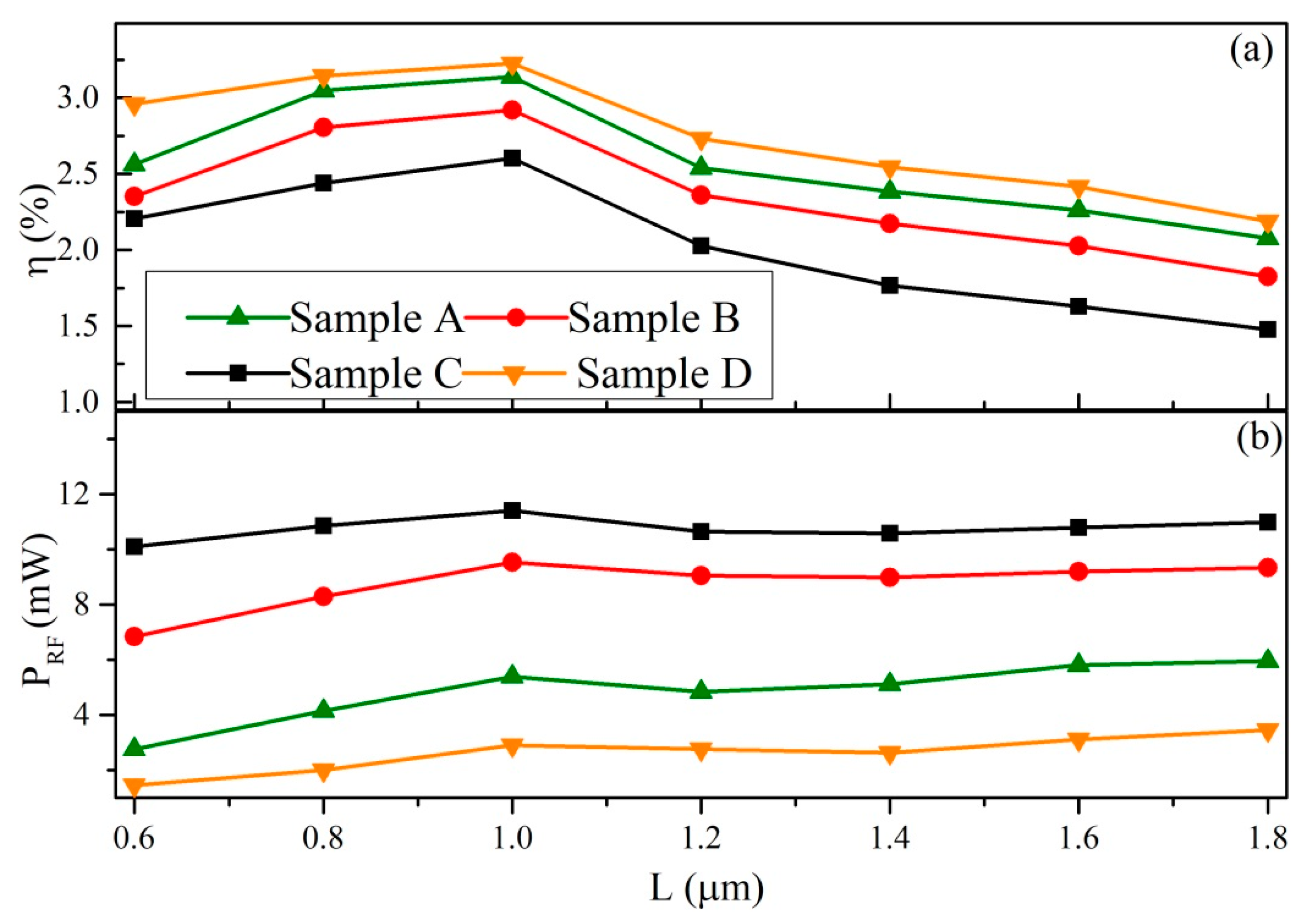
As we changed the position of the trench anode electrode, L1 and L2 changed accordingly. We set L2 = nL1, and L1 = L, where n is a positive integer. First we analyzed the samples as n = 1, that is, the anode contact was set at the center of the devices. The SPD with different numbers of 2DEG channels from 1–3, were named sample A–C. For each sample, the channel length L ranged from 0.6 to 1.8 µm, at a step of 0.2 µm. The regular single-2DEG-channel planar Gunn diode without a trench anode (sample D) was also analyzed as a reference, the channel length of which was also set to be L.
The results (RF-to-DC efficiency η versus the channel length L and RF output power P
RF versus L) are plotted in
Figure 2. As shown in
Figure 2, η decreases with the number of the 2DEG channels. The curves of η versus L for all the samples show the same trend. Both η and P
RF reach the value peaks at L = 1.0 µm. When the channel length L is shorter than 1.0 µm, the domain leaves the anode electrode before it grows mature, which results in lower η and P
RF. However, if the L is longer than 1.0 µm, the domain grows mature before reaching the anode electrode, which results in invalid growing space and, therefore, deteriorates the noise performance. For the 1.0-µm diode, the dipole domain grows to its mature size almost exactly as it reaches the anode electrode. Therefore, the highest operation performance is achieved in the diode of 1.0 µm.
The P
RF of 1.0-µm-Sample A was 5.48 mW, nearly twice of that of Sample D. This is because the trench anode divided the single 2DEG channel into two equal parallel channels. To further enhance the output power of SPD, we increased the number of AlGaN/GaN heterojunctions to achieve more parallel 2DEG channels.
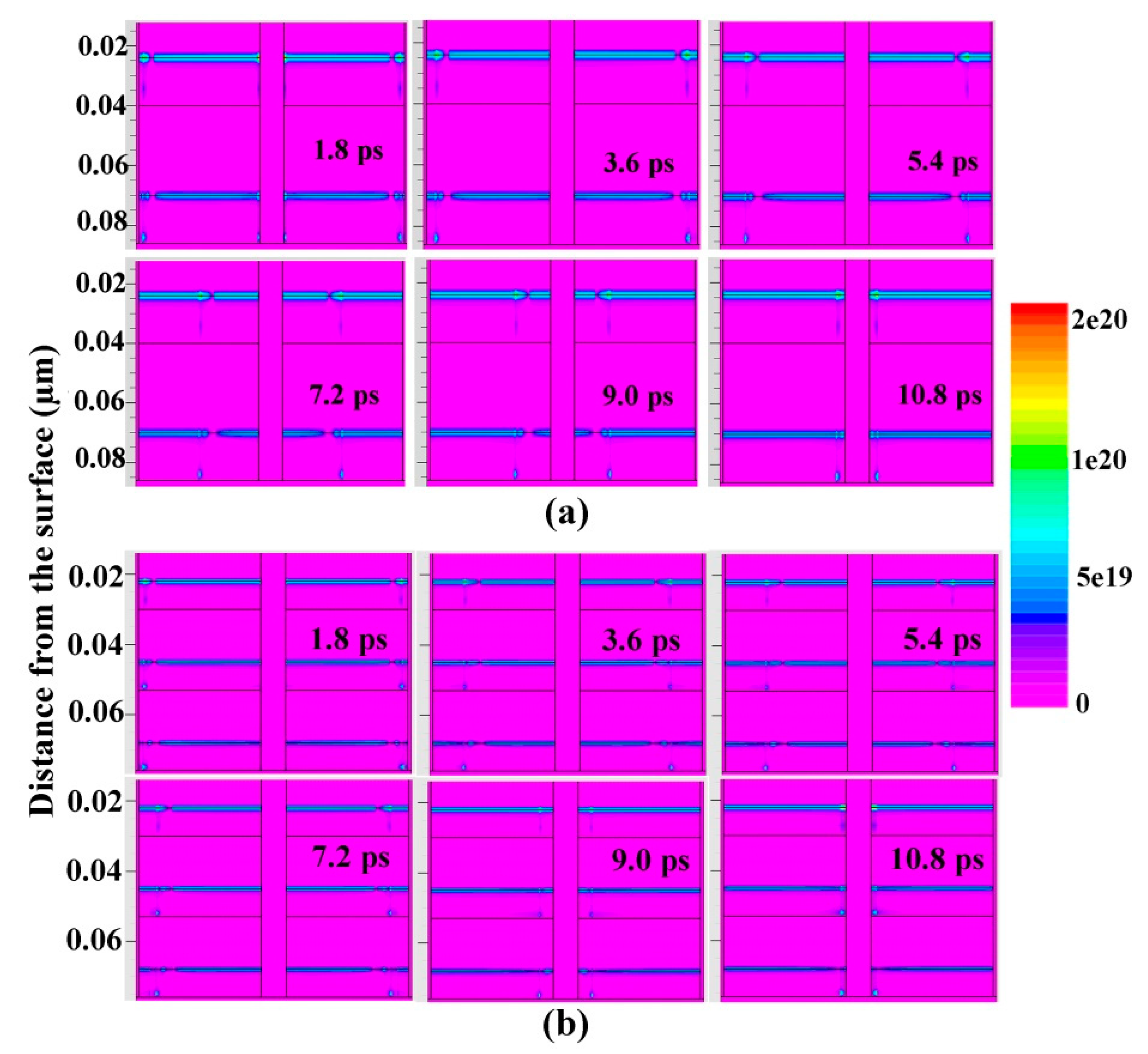
Figure 3a,b gives the electron tracks derived at the same time steps inside one oscillation circle from 1.0 µm-Sample B and Sample C respectively. Sample B contains two AlGaN/GaN heterojunctions, which can be equivalent to four 2DEG channels. Similarly, Sample C is equivalent to six 2DEG channels. As illustrated in
Figure 3, all the 2DEG channels were equal in length and independent of each other. In each channel, dipole domains form near the cathode contact and travel towards the anode contact without interfering with each other. Finally, all domains gradually disappear from anode contact at the same pace and a new oscillating circle repeats. The synchronization of electron domains inside each channel leads to a quasi-sine oscillating current wave; therefore, the fundamental frequency is enhanced. Ideally, since Sample B has four equal channels, its P
RF should be four times of that of 1.0-µm-Sample D. However, based on
Figure 2, P
RF of Sample B was 9.59 mW, only 3.2 times of that of Sample D. Furthermore, the efficiency η of sample B and C was also lower than Sample D. This is because in the multi-2DEG-channel structure, the electron concentration deeper in the channel is lower than in the upper channel. This easily results in the inconsistency of the electron domain in each channel, which will increase the non-linearity of the quasi-sine oscillating current wave, and leads to lower η and lower total oscillation power.
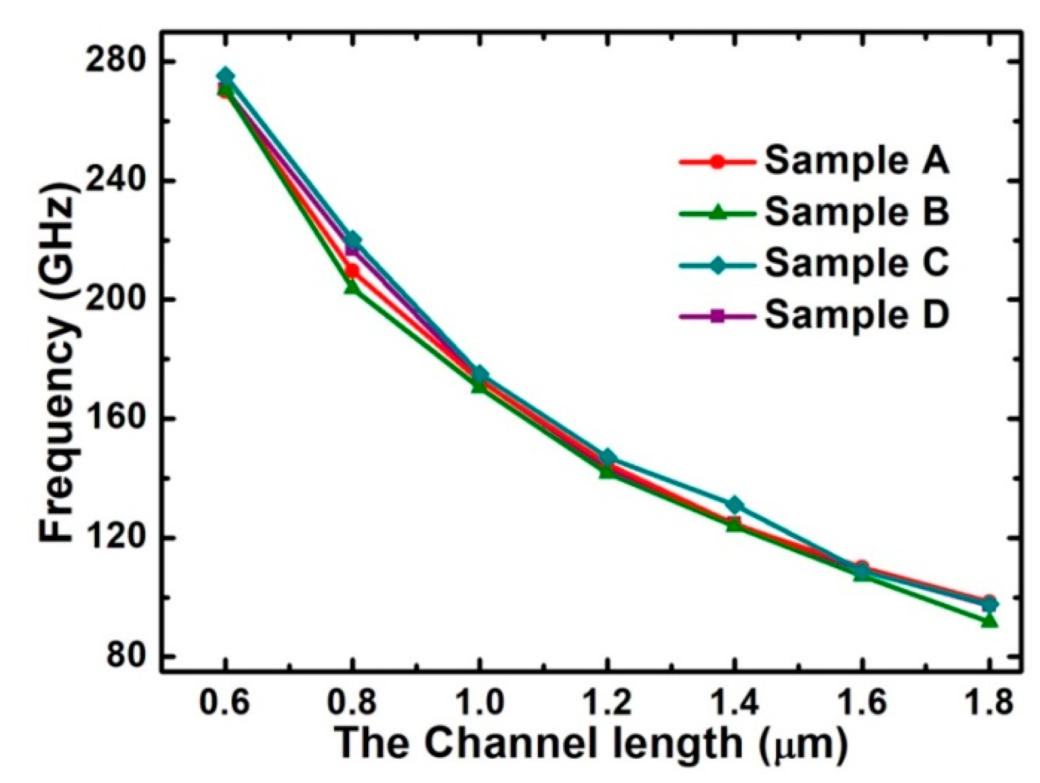
In addition, the results of frequency f versus channel length L for all the samples are plotted in
Figure 4. All the curves have the same trend and almost overlap, which basically follows the empirical formula: f = v
ave/L, where v
ave is the average velocity for the electron domain. For Sample A, the frequency is about 270.64 GHz when L = 0.6 µm and 172.94 GHz when L = 1.0 µm.
We also studied the asymmetric self-parallel diodes with different L
1 and L
2, where L
2 should be an integral multiple (
n) of L
1, that is, L
2 =
nL
1 (
n ≥ 2). In order to ensure that the electric field along the 2DEG-channel stays within the normal operating range, an appreciate voltage of V
1 should be applied across the cathode electrode C
1 and anode electrode A, and accordingly a voltage of
nV
1 should be applied across C
2 and A. We first studied the devices with L
1 = 0.6 µm and L
2 = 1.2 µm = 2 L
1.
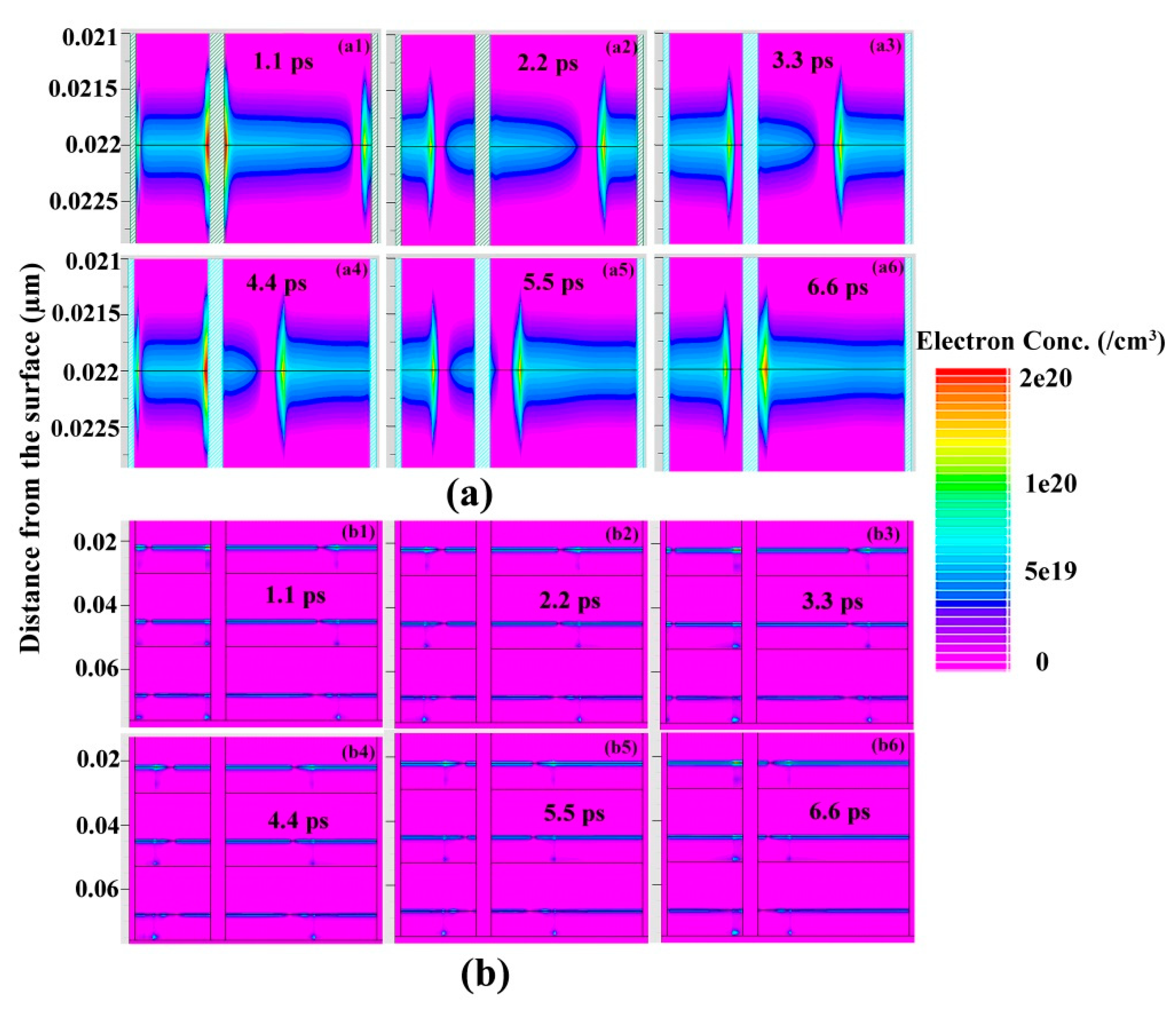
Figure 5a,b gives the schematic of the formation process of the electron dipoles in asymmetric single-2DEG-channel SPD and the triple-channel SPD respectively, from which we can see that the electron domains in the shorter channels repeated two circles, while the electron domains in the longer channels complete one circle. More specifically, from
Figure 5(a1–a3), we can see that the electron domain in the left channel has disappeared from the anode, while the domain in the right channel just approached the central position of the channel. In
Figure 5a4, a new dipole domain forms inside the left channel and the domain in the right channel continues to grow up as moving to the anode.
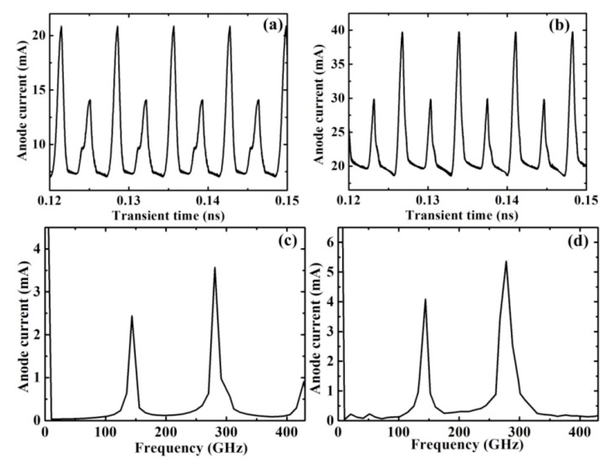
Figure 5(a5,a6) shows the process of disappearing of the two domains in both channels as they approach the anode side. The disappearance of the electron domain in the long channel represents a complete oscillation circle. The unsynchronized electronic domain motion results in the non-linearity of the RF current, as shown in
Figure 6, and the oscillation current wave and frequency spectrum of the 0.6–1.2-µm asymmetrical single-2DEG-channel and triple-2DEG-channel SPDs.
Figure 6 shows that there are two peaks in the oscillation current wave in both diodes and the second-harmonics are greatly enhanced. As shown in
Figure 6a,b, the smaller current peak is generated by the disappearance of the domain in the shorter channel, while the larger peak is due to the disappearance of the domain in the longer channel. For the single-2DEG-channel SPD, f of 280.77 GHz, η of 1.79%, and P
RF of 2.19 mW is achieved at the second harmonic. Correspondingly, P
RF increases to 6.02 mW, while f changes slightly at second harmonic in the triple-2DEG-channel SPD.
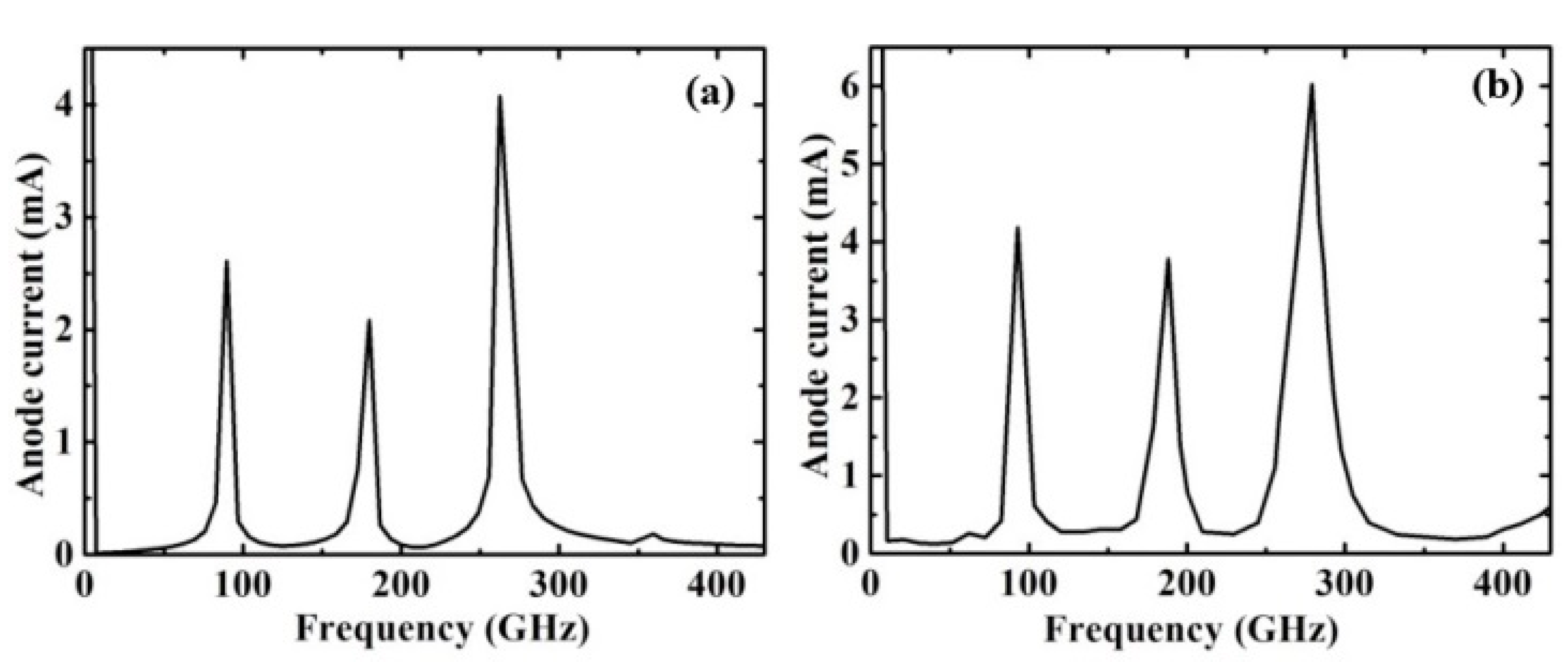
We further verified the motion of the electron domains in the multi-2DEG-channel SPD as L
2 = 1.8 µm = 3L
1. Similarly, before the dipole domain of the right channels leaves the anode electrode, the formation and movement of the electron domain repeat almost three circles in the shorter channel, which results in three current peaks in the oscillation current waves. Therefore, as shown in
Figure 7, the third harmonic component is greatly enhanced in both SPDs at the frequency of around 280 GHz.
Based on the research above, we reach the conclusion that in the asymmetric SPD, when L2 = nL1, the total number of the harmonic waves generated is equal to n. Highest output characteristics are received at the Nth harmonic component and its frequency is mainly determined by the L1.
4. Conclusions
In this paper, in order to realize the simultaneous enhancement of “oscillation power and frequency” of the planar Gunn diode, we propose the multi-2DEG-channel self-parallel diode (SPD) for the first time, and present a microscopic analysis on electron movements and RF characteristics of SPD. A trench anode is etched through 2DEG channels and breaks the longer 2DEG channel into several shorter channels. As a result, one regular Gunn diode is equal to several diodes in parallel. Therefore we name such diode a self-parallel Gunn diode (SPD).
In a symmetric multi-2DEG-channel SPD, dipole domain forms and travels in each channel without interference; therefore, the oscillation power is nearly multiplied as compared with the regular diode. We also analyze the complicated physical mechanism of the asymmetric multi-2DEG-channel SPD, where L2 = n L1 = nL (where n is an positive integer and n ≥ 2). Based on the simulation results, n circles of the electron domain in shorter channels approximately equal one circle of the electron domain in the longer channels, which results in n current peaks in the current waveforms and n harmonic components. The highest output power and efficiency are achieved on the nth harmonic, and its frequency is determined by L1.
Asymmetric SPD can not only generate several harmonic components, but also offers an easy transfer between two different fundamental frequencies. In addition, based on SPD structure, we can do further studies on the coupling mechanism of more complex electronic domains, which will provide theoretical guidance for designing and optimizing Gunn diodes.


