Article

Configurational Effects on Strain and Doping at Graphene-Silver Nanowire Interfaces

Department of Physics and Astronomy, University of Sussex, Brighton BN1 9RH, UK
*
Authors to whom correspondence should be addressed.
Appl. Sci. 2020, 10(15), 5157; https://doi.org/10.3390/app10155157
Submission received: 30 June 2020 / Revised: 23 July 2020 / Accepted: 24 July 2020 / Published: 27 July 2020

Abstract

:
Graphene shows substrate-dependent physical and electronic properties. Here, we presented the interaction between single-layer graphene and silver nanowire (AgNW) in terms of physical straining and doping. We observed a snap-through event for single-layer graphene/AgNW at a separation of AgNWs of 55 nm, beyond the graphene suspended over the nanowires. The adhesion force between the Atomic Force Microscopy (AFM) tip apex and the suspended graphene was measured as higher than the conformed one by 1.8 nN. The presence of AgNW modulates the Fermi energy level of graphene and reduces the work function by 0.25 eV, which results in n-type doping. Consequently, a lateral p-n-p junction is formed with single AgNW. The correlation Raman plot between G-2D modes reveals the increment of strain in graphene of 0.05% due to the curvature around AgNW, and 0.01% when AgNW lies on the top of graphene. These results provide essential information in inspecting the physical and electronic influences from AgNW.

1. Introduction

Graphene has always been a promising material for sensors, supercapacitors, and optoelectronics application by virtue of its high electrical conductivity, optical transmittance, and large surface area [1,2]. In recent years, the incorporation of silver nanowires (AgNWs) into graphene has compelled substantial attention due to the presence of surface plasmon resonance (SPR), which boosts the performance of photovoltaic devices [3], as well as the conductivity enhancement in the graphene-based transparent electrode [4]. Graphene can also act as a protective layer to AgNW with minimal disruption to the light transmittance [5]. While the benefit appears to be considerable, one should also inspect the physical and chemical influences, be it advantageous or disadvantageous, due to the addition of AgNW.
The hybrid system of graphene and AgNW can be regarded as textured surface and differentiated into two stacking arrangements: 1) graphene (Gr)/ silver nanowire (AgNW), where graphene covers the individual nanowire and induces strain at the curvature; and 2) AgNW/Gr, where the nanowire lies on the top of the graphene sheet, which generates less strain but some extension of carbon-carbon bond. Literature reveals the induced strain enhances electron–phonon coupling and potentially turns graphene into a Bardeen–Cooper–Schrieffer (BCS) superconductor [6]. Uniform uniaxial strain may also tune the electronic structure of graphene by shifting the Dirac cone and Landau quantization, which is crucial to explore the new field ‘’straintronics’’ where strain is engineered to achieve innovative applications [7,8]. Considering the work function difference between graphene and AgNW, electron (hole) will in general transfer from lower (higher) work function material to higher (lower) work function material [9]. This n-type (p-type) doping creates a p-n junction, which possesses peculiar properties such as quantum interference and Klein tunnellin [10,11]. Hence, understanding the strain and doping of graphene induced by the sandwiching of AgNW is indispensable.
The strain and doping configuration of graphene with the incorporation of silver nanostructure has been broadly studied in Raman spectroscopy, yet the conclusions are conflicting. Syed et al. [12] recorded stiffening of G mode and 2D mode due to embedding of silver nanoplates and suggested p-doping in graphene, while Wu and coworkers [13] observed upshift of G mode but downshift of 2D mode in graphene-covered silver nanoparticles (Gr/AgNPs) and claimed n-doping. Similar disagreement in doping direction can also be found in silver nanoparticles-stacked graphene (AgNPs/Gr) [3,14], and whether tensile or compressive strain is induced by the sandwiched AgNPs is still under dispute [3,13,14]. This contradiction arises mainly from the lack of a universal decoupling methodology of strain and doping from the Raman modes. The graphene heterostructure with AgNW, another family member in silver nanostructure, is rarely investigated; it is therefore essential to develop a comprehensive approach to study the strain and doping in Gr-AgNW system.
In the present work, we prepared two hybrid systems of single layer graphene and AgNW in different stacking orders, Gr/AgNW and AgNW/Gr, to investigate the graphene-silver interaction in different configurations. In both stacking arrangements, a similar magnitude of drop in work function in graphene has been observed by Kelvin probe force microscopy (KPFM). It leads to generation of lateral p-n-p junction as Gr/indium tin oxide (ITO)-Gr/AgNW/ITO-Gr/ITO. Subsequently, we demonstrated decoupling of strain and doping in our hybrid structure from the method developed by Lee et al. [15], and recognised that AgNWs (≈ 20 nm in height) exert more influence on tensile strain than charge transfer in both stacking order.

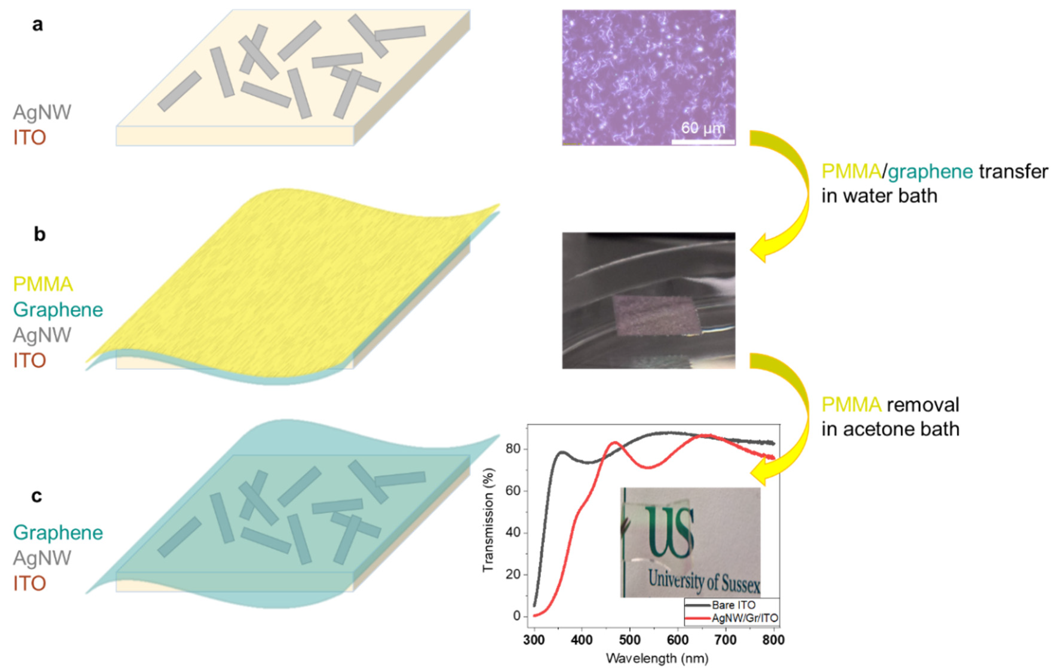
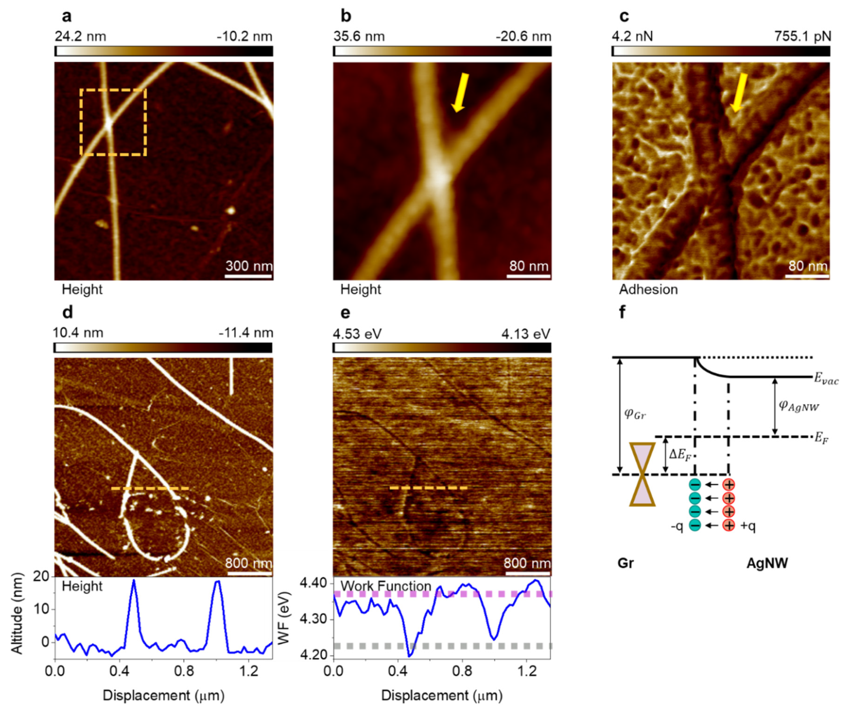
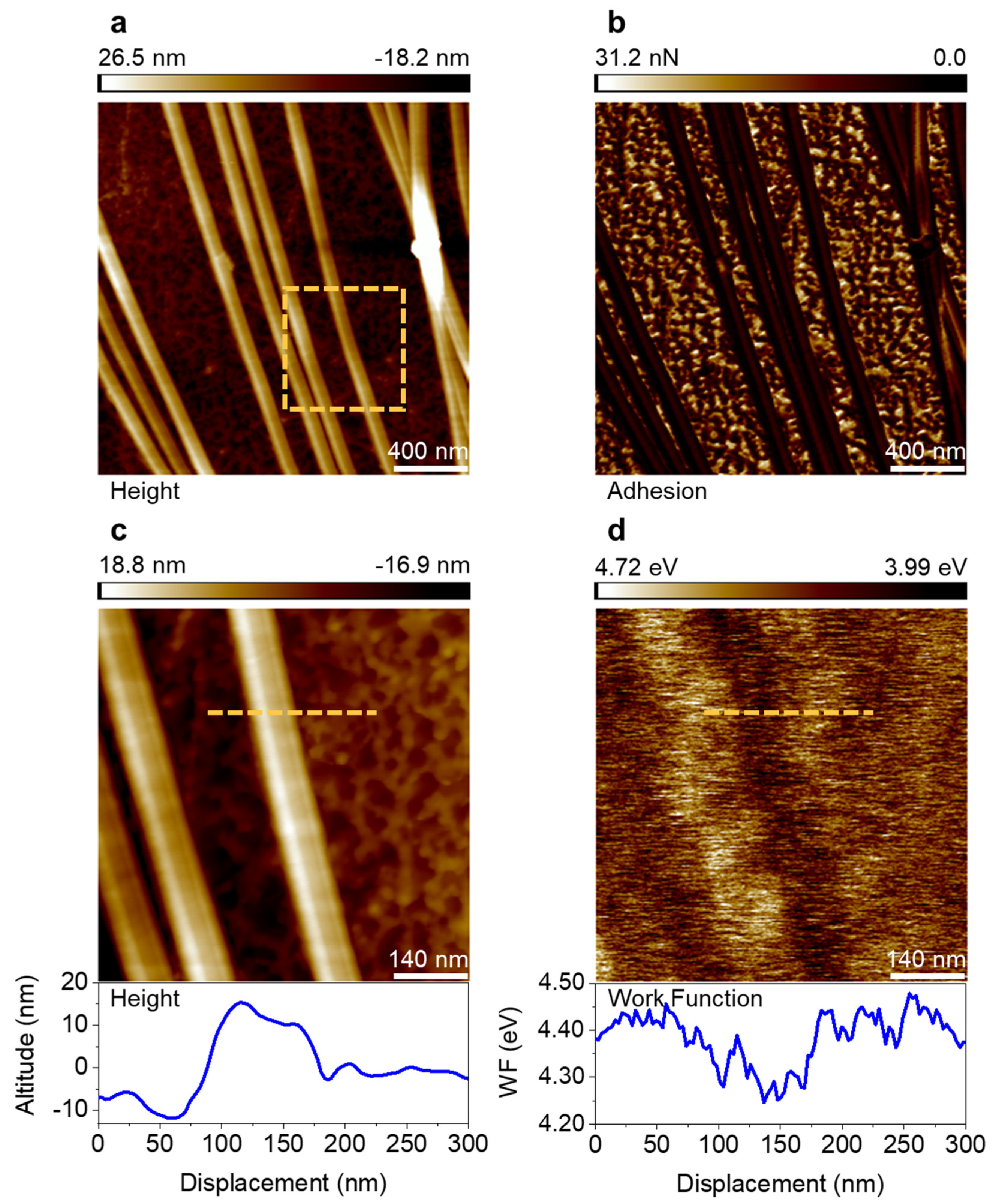
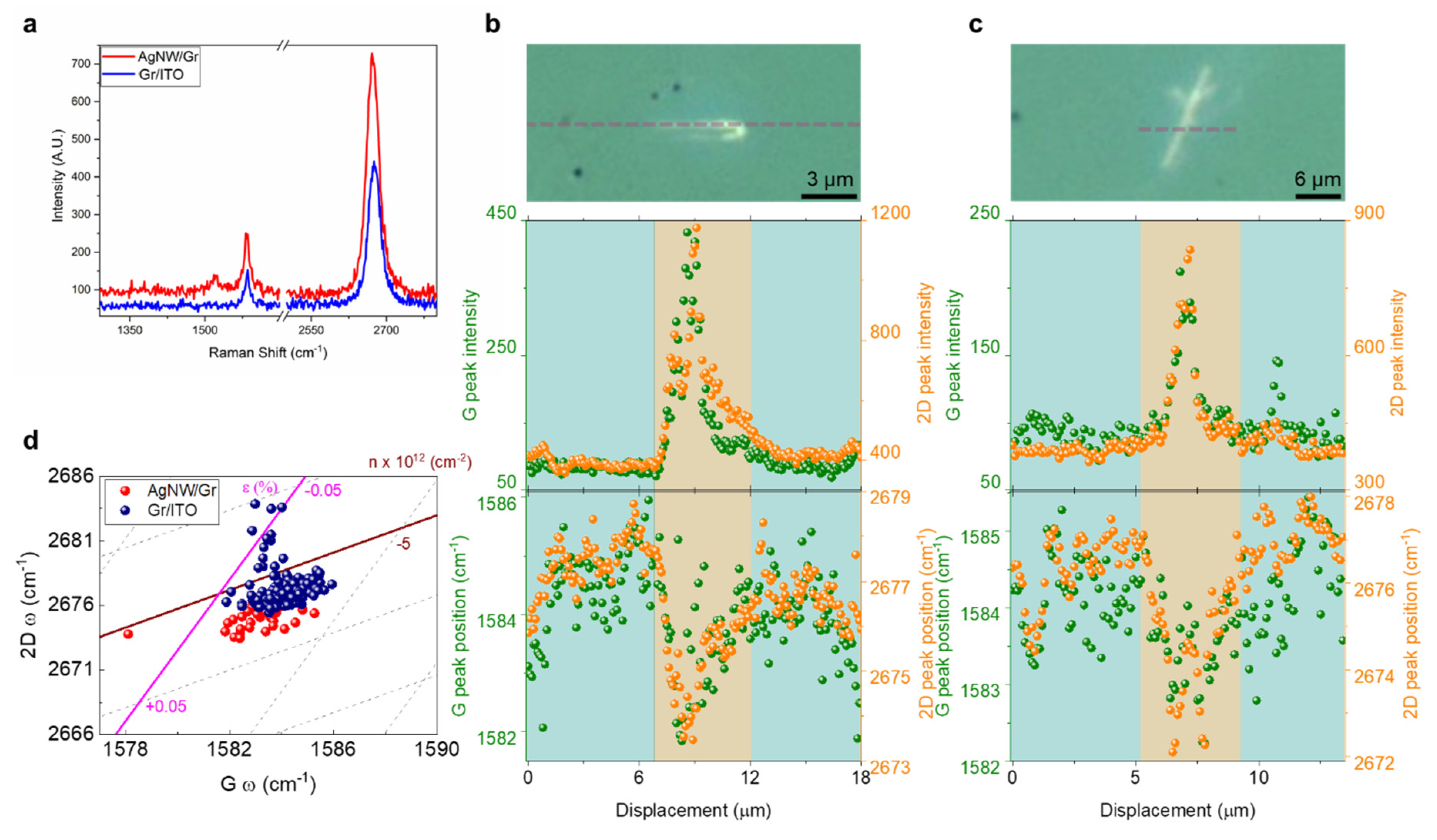
2. Results and Discussion

The fabrication of the Gr/AgNW heterostructure (Figure 1) involves air-spraying of AgNW on ITO substrate and subsequent deposition of Poly(methyl methacrylate) (PMMA)/Gr composite by wet transfer technique [16]. The uppermost PMMA is then removed by immersion in acetone bath, resulting in sole coverage of monolayer graphene on the AgNW network. The other stacking arrangement of AgNW/Gr heterostructure is simply fabricated by spraying AgNW solution over graphene. After the deposition of AgNW and graphene, the light transmittance reduces up to 10% between wavelengths of 488 and 650 nm (Figure 1c), indicating the graphene and AgNW layer permit sufficient light transmission for the function of optoelectronic devices.
In the Gr/AgNW system, conformation of graphene over the AgNW network (Figure 2a) is indicated by the morphology studies with atomic force microscopy. Substantial separation of two AgNWs (> 100 nm) allows graphene to follow the curvature and adhere to the ITO substrate between two nanowires, thanks to the low bending rigidity of single layer graphene (7.1 eV) [17]. However, closely spaced AgNWs reduce the tendency of graphene conformation and eventually result in snap-through transition, where graphene is suspended and fails to touch the substrate (indicated by yellow arrow in Figure 2b). This snap-through transition can also be confirmed by the adhesion force map in Figure 2c, which reveals the contrast in adhesion force between silica tip apex and Gr/ITO (3.7 ± 0.2 nN), Gr/AgNW (1.3 ± 0.1 nN), and graphene on constrained area indicated by the yellow arrow (3.1 ± 0.2 nN). The adhesion force in 2D materials depends not only on the material surface chemistry, but also on the interfacial interaction between graphene and its subsurface, which regulates the contact area between tip apex and graphene. Compared to Gr/ITO, where the flat monolayer readily favours the contact, in Gr/AgNW, the conformed strain at the curvature of AgNW reduces the contact area in graphene, and hence its adhesion force is significantly lower than that of Gr/ITO. Given the adhesion force of graphene on constrained area is between that of Gr/ITO and Gr/AgNW, it is reasonable to suspect graphene is suspended between two AgNWs at that region. This snap-through transition occurs due to a balance between the surface adhesion energy and the conformed strain energy [18], which, according to our enlarged AFM image of intersection of two AgNWs (Figure 2b,c), takes place at the separation distance of 50 ± 5 nm.
The surface potential of Gr/AgNW heterostructure is studied by Kelvin probe force microscopy (KPFM) as depicted in Figure 2d,e, which involves scanning of cantilever over the surface with an optimised height (lift height = 15 nm) to measure the contact potential difference (CPD) between the conductive tip and the hybrid surface. The work function φ can then be determined by Equation (1)
e · ( C P D ) = φ s a m p l e φ t i p
where e represents the elementary charge. Highly oriented pyrolytic graphite (HOPG) ( φ = 4.66   e V ) serves as a reference for calibration of φ t i p , which in turn permits the calculation of φ s a m p l e at examined region. φ is defined as the electrostatic potential between near-surface vacuum energy and the Fermi level (EF). Hence, it can be regarded as the ability to bind the electron at the interface during contact, and electron charge will flow from lower φ material to higher φ material [9]. We observe a drop in φ of 0.15 ± 0.03 eV at the Gr/AgNW region compared to the surrounding Gr/ITO, which implies graphene gains electrons from AgNW and EF of graphene moves towards conduction band as illustrated in the schematic band diagram (Figure 2f). As graphene is previously p-doped in the graphene/ITO heterostructure [19], the insertion of AgNW between graphene and ITO forms a p-n-p junction due to modulation in the EF of graphene.
The physical and electronic modification to graphene by AgNW is investigated by Raman spectroscopy, where the typical Raman spectra are illustrated in Figure 3a. Graphene Raman modes comprise G peak and 2D peak, which are located at 1585 cm−1 and 2680 cm−1, and respectively correspond to the first-order double-degenerated scattering process due to E2g symmetry and the second-order phonon mode between two iTO phonons [20]. D peak, situating at 1340 cm−1, requires structural defects for its activation. The absence of prominent D peak in the Raman spectrum in Figure 3a indicates minimal density of defects. G and 2D modes are sensitive to strain and doping, while the effect of strain (doping) is more significant to the shift of 2D (G) peak [15]. An intensity enhancement of both peaks are observed at the graphene-covered AgNW region compared to graphene only, suggesting a surface-enhanced Raman scattering (SERS) effect [21]. SERS originates from the resonant response from localised surface plasmons, where the metal nanostructure serves as a hotspot to strengthen the surrounding electric field [22]. The intensity ratio I2D/IG being larger than 1 also confirms the enveloping graphene is monolayer [23]. Apart from the intensity enhancement, both G and 2D peaks also red shift at the AgNW region, revealing an influence on strain or doping by the curvature of the nanowire.
A clear transition of peak intensity and peak position from the bare graphene to the AgNW-embedded graphene is reflected by a thorough investigation of a Raman line map across the AgNW along the axial direction (Figure 3b) and the transverse direction (Figure 3c). We observe an increase of G peak intensity and 2D peak intensity by 50%, and a redshift of G ω (G peak position) and 2D ω (2D peak position) of 4 cm−1 and 11 cm−1, respectively. The peak shifts can be correlated with the induced strain ε and the charge carrier density n of graphene by
( ω G ω 2 D ) = T ( ε n )
where
T = ( 2 γ G ω G 0 k G 2 γ 2 D ω 2 D 0 k 2 D )
γ is the Grüneisen parameter, k is the doping shift constant, and ω 0 is the no-strain no-doping peak position. Literature reveals γ G = 1.95, γ 2 D = 3.15, k G = 1.407 × 10 12   c m 1 , and k 2 D = 0.285 × 10 12   c m 1 [15,24]. This linear transformation of ε - n space to the space of G ω and 2D ω realises a correlation plot of 2D ω against G ω , with inclined isolines (grey dashed lines) representing equal strain and doping. As shown in Figure 3d, the flat graphene exhibits a tensile strength of 0.01%, while the graphene-covered AgNW region depicts a strain generation of 0.06%, implying a tension increase by 5 folds due to the embedded AgNW. This result shows that the conforming of graphene on the curvature of AgNW induces strain.
Similar morphology studies are performed in the different stacking arrangement of AgNW/Gr. We observed comparable height of graphene in covered and uncovered AgNW (Figure 4b,c), which indicates graphene attachment on AgNW does not lead to significant alternation in topography. Nevertheless, uncovered AgNW influences the adhesion force map and results in a drop in adhesion force of 30 nN due to different hetero interactions between uncovered AgNW and the tip apex. The surface potential analysis in Figure 4c,d demonstrates a reduction of φ of 0.2 eV across the AgNW region compared to the graphene substrate, which is in consonance with the Gr/AgNW system. In both stacking arrangements of graphene and AgNW, the local p-n-p junction has been observed.
The effect on the strain and spatial charge distribution in AgNW/Gr heterostructure is also studied by Raman spectroscopy, where AgNW region displays SERS effect and redshifts in both G and 2D peaks compared to that of the bare graphene (Figure 5a), similar to the Gr/AgNW system. Line maps across the AgNW along the axial direction (Figure 5b) and the transverse direction (Figure 5c) conveys an increase of G and 2D peak intensity up to 800% and 200% in the AgNW region, revealing a more notable SERS effect than the Gr/AgNW heterostructure. In addition to the 2.7% light absorbance of graphene, which should play minimal role, we suspect this phenomenon is due to curvature-induced strong interaction between graphene and AgNW, which leads to reduction of hot spots for SERS to take place in Gr/AgNW system [14,25]. It is also noteworthy that additional peak at around 1520 cm−1 is observed in AgNW/Gr spectrum, which arises from the PVP coating residue around AgNW [26].
The topping of AgNW induces redshift of G ω and 2D ω by 3 cm−1 and 5 cm−1, respectively, compared to the flat graphene, which is, upon constructing a correlation plot with parallel strain and doping axes in Figure 5d, responsible for a tensile strain of 0.01% induced by the nanowires. It clearly shows that AgNW lying on top does not induce any profound change in tensile strain in graphene but a slight extension of carbon–carbon bonds as compared to graphene over ITO surface. In both AgNW/Gr and Gr/AgNW system, the Raman analysis shows dominant response from strain than doping.

3. Conclusions

The graphene–AgNW interaction is studied in two different stacking arrangements, where AgNW is placed beneath and above monolayer graphene. The presence of AgNW reduces the work function in graphene by modulation of Fermi energy level and induces n-type doping. This arrangement leads to the formation of local p-n-p junctions for both stacking arrangements. Graphene as a top layer exerts tensile strain up to 0.05% due to the curvature around AgNW. Nevertheless, a lower strain of 0.01% is observed when the graphene is placed between ITO and AgNW. Our results show that the combination of KPFM and Raman spectroscopy can thoroughly inspect the physical and electronic influences from the addition of AgNW to graphene, which provides useful information for devices using hybrid structure of these two 2D materials.

4. Material and Methods

Sample fabrication: Gr/AgNW/ITO: ITO substrate (2 cm × 1 cm) is cut and cleaned with ethanol and IPA, before air-spraying of 2 mL (0.25 mg/mL) AgNW/water solution, which is diluted from the stock solution from Sigma (5 mg/mL). Graphene, initially sandwiched between PMMA and polymer, is commercially obtained from ACS Material, which is then transferred to AgNW/ITO by Trivial Transfer Graphene (TTG) technique under the following procedure. The PMMA/Gr/polymer hybrid is immersed in deionised water to release the polymer, and the remaining PMMA/Gr is left in water for 2 hours before transferring to AgNW/ITO substrate to form PMMA/Gr/AgNW/ITO. After the transfer, the sample is dried naturally for 30 minutes and then baked in oven at 100 °C for 30 minutes. The sample is then immersed in acetone bath for 30 minutes to dissolve the surface layer PMMA and dry in oven at 40 °C for 20 minutes to assemble the final Gr/AgNW/ITO hybrid. AgNW/Gr/ITO: The sample is similarly fabricated as in Gr/AgNW/ITO but the transfer of graphene into ITO takes place before the air-spraying of AgNW.
UV-vis characterisation is performed by Shimadzu UV3600Plus UV−vis−NIR at wavelength between 300 nm and 800 nm. AFM and KPFM characterisation is carried out by Bruker Dimension Icon with advanced operation mode of PF-QNM (PeakForce-Quantitative nanomechanical) and PF-KPFM (PeakForce-Kelvin Probe Force Microscopy), respectively, to measure the topography, adhesion, and surface potential. Work function is measured at the lift height of 15 nm. Raman spectroscopy is performed by Renishaw inVia™ confocal Raman microscope with 0.8 cm−1 spectral resolution. 532 nm laser (type: solid state, model: RL53250) with 5mW laser power and 1800 mm−1 grating is used. The peak position and intensity are then estimated by Lorentz fitting.

Author Contributions

Formal analysis, P.L.; Investigation, F.L.; Project administration, A.B.D.; Supervision, M.T. and A.B.D. All authors have read and agreed to the published version of the manuscript.

Funding

The authors gratefully acknowledge for funding support from Advanced Material Development Ltd.in carrying out the work.

Acknowledgments

MT would like to acknowledge University of Sussex strategic development fund.

Conflicts of Interest

The authors declare no conflict of interest.

References

  1. Bonaccorso, F.; Sun, Z.; Hasan, T.; Ferrari, A.C. Graphene photonics and optoelectronics. Nat. Photonics 2010, 4, 611. [Google Scholar] [CrossRef] [Green Version]
  2. Wang, Y.; Shi, Z.; Huang, Y.; Ma, Y.; Wang, C.; Chen, M.; Chen, Y. Supercapacitor Devices Based on Graphene Materials. J. Phys. Chem. C 2009, 113, 13103–13107. [Google Scholar] [CrossRef]
  3. Gong, T.; Zhang, J.; Zhu, Y.; Wang, X.; Zhang, X.; Zhang, J. Optical properties and surface-enhanced Raman scattering of hybrid structures with Ag nanoparticles and graphene. Carbon 2016, 102, 245–254. [Google Scholar] [CrossRef]
  4. Xu, G.; Liu, J.; Wang, Q.; Hui, R.; Chen, Z.; Maroni, V.A.; Wu, J. Graphene: Plasmonic Graphene Transparent Conductors (Adv. Mater. 10/2012). Adv. Mater. 2012, 24, OP70. [Google Scholar] [CrossRef]
  5. Li, X.; Li, J.; Zhou, X.; Ma, Y.; Zheng, Z.; Duan, X.; Qu, Y. Silver nanoparticles protected by monolayer graphene as a stabilized substrate for surface enhanced Raman spectroscopy. Carbon 2014, 66, 713–719. [Google Scholar] [CrossRef]
  6. Si, C.; Liu, Z.; Duan, W.; Liu, F. First-principles calculations on the effect of doping and biaxial tensile strain on electron-phonon coupling in graphene. Phys. Rev. Lett. 2013, 111, 196802. [Google Scholar] [CrossRef]
  7. Si, C.; Sun, Z.; Liu, F. Strain engineering of graphene: A review. Nanoscale 2016, 8, 3207–3217. [Google Scholar] [CrossRef]
  8. Mueller, N.S.; Heeg, S.; Alvarez, M.P.; Kusch, P.; Wasserroth, S.; Clark, N.; Schedin, F.; Parthenios, J.; Papagelis, K.; Galiotis, C. Evaluating arbitrary strain configurations and doping in graphene with Raman spectroscopy. 2D Materials 2017, 5, 015016. [Google Scholar] [CrossRef]
  9. Palermo, V.; Palma, M.; Tomović, Ž.; Watson, M.D.; Friedlein, R.; Müllen, K.; Samorì, P. Influence of Molecular Order on the Local Work Function of Nanographene Architectures: A Kelvin-Probe Force Microscopy Study. ChemPhysChem 2005, 6, 2371–2375. [Google Scholar] [CrossRef]
  10. Young, A.F.; Kim, P. Quantum interference and Klein tunnelling in graphene heterojunctions. Nat. Phys. 2009, 5, 222–226. [Google Scholar] [CrossRef] [Green Version]
  11. Abanin, D.A.; Levitov, L.S. Quantized transport in graphene pn junctions in a magnetic field. Science 2007, 317, 641–643. [Google Scholar] [CrossRef] [Green Version]
  12. Syed, S.R.; Lim, G.-H.; Flanders, S.J.; Taylor, A.B.; Lim, B.; Chon, J.W.M. Single layer graphene band hybridization with silver nanoplates: Interplay between doping and plasmonic enhancement. Appl. Phys. Lett. 2016, 109, 103103. [Google Scholar] [CrossRef]
  13. Wu, T.; Shen, H.; Sun, L.; Cheng, B.; Liu, B.; Shen, J. Facile synthesis of Ag interlayer doped graphene by chemical vapor deposition using polystyrene as solid carbon source. ACS Appl. Mater. Interfaces 2012, 4, 2041–2047. [Google Scholar] [CrossRef]
  14. Sun, H.-B.; Fu, C.; Xia, Y.-J.; Zhang, C.-W.; Du, J.-H.; Yang, W.-C.; Guo, P.-F.; Xu, J.-Q.; Wang, C.-L.; Jia, Y.-L. Enhanced Raman scattering of graphene by silver nanoparticles with different densities and locations. Mater. Res. Express 2017, 4, 025012. [Google Scholar] [CrossRef]
  15. Lee, J.E.; Ahn, G.; Shim, J.; Lee, Y.S.; Ryu, S. Optical separation of mechanical strain from charge doping in graphene. Nat. Commun. 2012, 3, 1024. [Google Scholar] [CrossRef] [Green Version]
  16. Ploss, R.S. Material Trivial Transfer Graphene. Google Patents No. US8906245B2, 19 December 2014. [Google Scholar]
  17. Lindahl, N.; Midtvedt, D.; Svensson, J.; Nerushev, O.A.; Lindvall, N.; Isacsson, A.; Campbell, E.E.B. Determination of the bending rigidity of graphene via electrostatic actuation of buckled membranes. Nano Lett. 2012, 12, 3526–3531. [Google Scholar] [CrossRef] [Green Version]
  18. Scharfenberg, S.; Mansukhani, N.; Chialvo, C.; Weaver, R.L.; Mason, N. Observation of a snap-through instability in graphene. Appl. Phys. Lett. 2012, 100, 021910. [Google Scholar] [CrossRef] [Green Version]
  19. Schlaf, R.; Murata, H.; Kafafi, Z.H. Work function measurements on indium tin oxide films. J. Electron Spectrosc. Relat. Phenom 2001, 120, 149–154. [Google Scholar] [CrossRef]
  20. Malard, L.M.; Pimenta, M.A.A.; Dresselhaus, G.; Dresselhaus, M.S. Raman spectroscopy in graphene. Phys. Rep. 2009, 473, 51–87. [Google Scholar] [CrossRef]
  21. Suzuki, S.; Yoshimura, M. Chemical stability of graphene coated silver substrates for surface-enhanced Raman scattering. Sci. Rep. 2017, 7, 14851. [Google Scholar] [CrossRef]
  22. Muntean, C.M.; Dina, N.E.; Coroş, M.; Toşa, N.; Turza, A.I.; Dan, M. Graphene/silver nanoparticles-based surface-enhanced Raman spectroscopy detection platforms: Application in the study of DNA molecules at low pH. J. Raman Spectrosc. 2019, 50, 1849–1860. [Google Scholar] [CrossRef]
  23. Ferrari, A.C.; Meyer, J.C.; Scardaci, V.; Casiraghi, C.; Lazzeri, M.; Mauri, F.; Piscanec, S.; Jiang, D.; Novoselov, K.S.; Roth, S. Raman spectrum of graphene and graphene layers. Phys. Rev. Lett. 2006, 97, 187401. [Google Scholar] [CrossRef] [Green Version]
  24. Jiang, T.; Wang, Z.; Ruan, X.; Zhu, Y. Equi-biaxial compressive strain in graphene: Grüneisen parameter and buckling ridges. 2D Materials 2018, 6, 015026. [Google Scholar] [CrossRef] [Green Version]
  25. Guo, C.; Zhang, J.; Xu, W.; Liu, K.; Yuan, X.; Qin, S.; Zhu, Z. Graphene-based perfect absorption structures in the visible to terahertz band and their optoelectronics applications. Nanomaterials 2018, 8, 1033. [Google Scholar] [CrossRef] [Green Version]
  26. Tan, X.; Wang, Z.; Yang, J.; Song, C.; Zhang, R.; Cui, Y. Polyvinylpyrrolidone-(PVP-) coated silver aggregates for high performance surface-enhanced Raman scattering in living cells. Nanotechnology 2009, 20, 445102. [Google Scholar] [CrossRef]
Figure 1. Stages of the preparation of graphene (Gr)/silver nanowire (AgNW) heterostructure. (a) Initially, AgNW is spray-coated on indium tin oxide (ITO) substrate. (b) Deposited AgNW is subsequently covered by Poly(methyl methacrylate) (PMMA)/Gr hybrid by wet transfer technique. (c) The PMMA layer is then removed in acetone bath and only the graphene monolayer remains on AgNW surface. The transparent hybrid layer of graphene-covered AgNW on ITO substrate shows the background of the logo of University of Sussex. There is reduction in the transmittance by 10% between 488 and 650 nm wavelength.
Applsci 10 05157 g001
Figure 2. Atomic force microscopy(AFM) and Kelvin probe force microscopy (KPFM) mapping of Gr/AgNW heterostructrue: (a) AFM topography of AgNW network under monolayer graphene displays an intersection of two AgNWs (marked by dashed square); (b) morphology; and (c) adhesion, which is further analyzed. Suspension of graphene near the crossing is observed (yellow arrow), and a drop in adhesion force is recorded at the AgNW region. (d) Topography and (e) work function of the heterostructure shows a reduction of work function across the AgNW region. The purple and grey dotted lines represent the average work function value of Gr/ITO and Gr/AgNW, respectively. The difference between two values is calculated to be 0.15 ± 0.03 eV. (f) Band diagram at Gr/AgNW interface. Charges are transferred from AgNW to Gr due to Fermi level difference.
Applsci 10 05157 g002
Figure 3. Raman spectroscopy of Gr/AgNW heterostructure (a) typical Raman spectrum of graphene-covered AgNW and graphene only region. Slight effect of surface-enhanced Raman scattering (SERS) and redshifts of G and 2D peak are observed in Gr/AgNW heterostructure. (b) Raman line map (indicated by the purple line) across the AgNW along the axial direction and (c) transverse direction. In both cases, the G and 2D peak intensity increases at the Gr/AgNW region (red colour in background), compared to the Gr/ITO region (blue colour in background). Redshifts of both peaks are also recognised at the AgNW region. (d) Strain and doping map of the above regions shows tensile strain of approximately 0.06% at the graphene-covered AgNW compared to graphene only region. Electron concentration is comparable within two regions.
Applsci 10 05157 g003
Figure 4. AFM and KPFM mapping of AgNW/Gr heterostructrue: (a) AFM topography and (b) adhesion force map of AgNW network above monolayer graphene. A reduction in adhesion is observed. (c) Morphology and (d) work function of AgNW/Gr system indicate a drop in 0.2 eV across the AgNW region.
Applsci 10 05157 g004
Figure 5. Raman spectroscopy of AgNW/Gr heterostructure. (a) Typical Raman spectrum of AgNW-covered monolayer graphene and graphene only region. A significant SERS effect is observed. (b) Raman line map (indicated by the purple line) across the AgNW along the axial direction and (c) transverse direction. In both cases, the G and 2D peak intensity increases at the AgNW/Gr region (red colour in background) compared to the Gr/ITO region (blue colour in background). (d) Strain and doping map of the above regions shows miniature tensile strength (0.01%) at the AgNW region compared to graphene only region. The difference in charge density is negligible.
Applsci 10 05157 g005

