1. Introduction
One of the features of our time is a wide application of digital systems in various spheres of human activity [
1,
2]. Modern digital systems include different combinational and sequential blocks [
3,
4]. The behaviour of a sequential block can be represented using the model of finite state machine (FSM) [
5,
6]. To improve characteristics of a digital system, it is necessary to improve such characteristics of FSMs as internal occupied resources, performance and power consumption. This necessity explains the continuous interest in developing methods aimed at optimizing these characteristics of FSM circuits. As a rule, the less internal occupied resources are used by an FSM circuit, the less power it consumes [
7]. So, it is very important to reduce internal occupied resources consumed by an FSM circuit.
A sequential block can be represented as either Mealy or Moore FSM [
5,
6]. There are thousands of monographs and articles devoted to problems of FSM circuits design. The vast majority of these works are devoted to Mealy FSMs. Based on this analysis, we have chosen Mealy FSM as the object of research in our current article.
To diminish the required internal occupied resources, it is necessary to take into account specifics of logic elements implementing FSM circuits [
8,
9]. Nowadays, field programmable gate arrays (FPGAs) [
10,
11,
12] are widely used in the implementation of digital systems [
9,
13,
14,
15]. Due to it, we choose FPGA-based FSMs as a research object in the given article. In this article, we consider a case when look-up table (LUT) elements are used to implement logic circuits of Mealy FSMs.
A LUT is a block having
inputs and a single output [
10,
12]. A single LUT allows implementing an arbitrary Boolean function having up to
arguments [
16,
17]. However, the number of LUT inputs is rather small [
10,
12]. This feature leads to the need of functional decomposition of systems of Boolean functions (SBFs) representing FSM circuits [
17,
18]. In turn, this leads to multi-level FSM circuits with complex systems of interconnections [
9].
One of the most crucial steps in the LUT-based design flow is the technology mapping [
19,
20,
21,
22,
23,
24,
25]. During this step, an FSM circuit is converted into a network of interconnected LUTs. The outcome of technology mapping determines resulting characteristics of an FSM circuit. These characteristics are strongly interrelated.
The internal occupied resources consumed by a LUT-based FSM circuit include LUTs, flip-flops, interconnections, circuit of synchronization, input-output blocks. Obviously, to reduce the amount of required resources, it is very important to reduce the LUT count in a circuit. As follows from [
26], the more LUTs are included into an FSM circuit, the more static power it consumes. Now, process technology has scaled considerably, with current design activity at 14 and 7 nm. Due to it, interconnection delay now dominates logic delay [
26]. As noted in [
16,
27], the interconnections are responsible for the consuming up to 70% on power. So, it is very important to reduce the amount of interconnections to improve the characteristics of FSM circuits.
As shown in [
26,
28], the value
provides an optimal trade-off for the occupied chip area, performance, and power consumption of a LUT. However, the complexity of FPGA-based projects is constantly growing [
9]. To overcome this contradiction, it is necessary to develop the methods of technology mapping that take into account rather small value of LUT’s inputs.
The main contribution of this paper is a novel design method aimed at reducing the number of LUTs in circuits of FPGA-based Mealy FSMs. The proposed approach is based on joint usage of two known methods of structural decomposition (replacement of inputs and encoding of collections of outputs). The method leads to FSM circuits having three levels of logic and regular system of interconnections. The proposed method allows obtaining FSM circuits with fewer LUTs compared to circuits based on either single-level or two-level FSM models. Our current study is focused in Xilinx solutions [
12].
The rest of the paper is organised as the follows.
Section 2 presents the theoretical background of Mealy FSMs and peculiarities of FPGAs.
Section 3 discusses the state of the art of FPGA-based technology mapping.
Section 4 describes the main idea of the proposed method. The synthesis example is shown in
Section 5.
Section 6 gives results of experiments conducted on standard benchmarks [
29]. A brief conclusion ends the paper.
2. Specifics of FPGAs and Mealy FSMs
The majority of modern FPGAs are organized using so called “island-style” architecture [
16,
28,
30]. They include different configurable logic blocks (CLBs) and a matrix of programmable interconnections [
10,
11,
12]. In this article, we consider CLBs consisting of LUTs and programmable flip-flops. To implement LUT-based circuits of sequential blocks, it is necessary to connect outputs of some LUTs with flip-flops [
5].
An extremely small amount of LUT inputs leads to the necessity of functional decomposition [
17] of functions representing combinational parts of FSMs. The functional decomposition produces multi-level circuits with irregular systems of interconnections. Such circuits resemble “spaghetti-type” programs [
28]. Using terminology from programming, we can say that the functional decomposition produces LUT-based circuits with “spaghetti-type” interconnections.
A Mealy FSM is defined as a vector
[
5], where
is a set of inputs,
is a set of outputs,
is a set of internal states,
is a function of transitions,
is a function of output, and
is an initial state. A Mealy FSM can be represented using different tools, such as: state transition graphs [
3,
5], binary decision diagrams [
31,
32], and-inverter graphs [
33], graph-schemes of algorithms [
5]. In this article, we use state transition tables (STTs) for this purpose.
An STT includes the following columns [
3,
5]:
is a current state;
is a state of transition (a next state); X
is a conjunction of inputs (or their compliments) determined a transition from
to
;
is a collection of outputs generated during the transition from
to
. The column
h includes the numbers of transitions (
). For example, the STT (
Table 1) represents some Mealy FSM
.
Using STT (
Table 1), the following parameters of
can be found: the number of inputs
, the number of outputs
, the number of states
, and the number of transitions
. Furthermore,
Table 1 uniquely defines the functions of transitions and output of FSM
.
To find SBFs representing an FSM circuit, it is necessary [
5]: (1) to encode states
by binary codes
; (2) to construct sets of state variables
and input memory functions (IMFs)
and (3) to transform an initial STT into a direct structure table (DST). States
are encoded during the step of state assignment [
3].
In this article, we use the state codes having the minimum possible number of state variables
R, where
This method is used, for example, in well-known academic system SIS [
34]. There are other approaches for state encoding where the number of state variables differs from (
1). For example, the academic system ABC [
33] of Berkeley uses one-hot state assignment with
.
State codes are kept into a state register (
). The
consists of R flip-flops with mutual inputs of synchronization (
Clock) and reset (
Start). For LUT-based FSMs, D flip-flops are used to organize state registers [
9]. The pulse
Clock allows the functions
to change the RG content.
To find functions representing an FSM circuit, it is necessary to create a direct structure table. A DST is an expansion of an STT by the columns with codes of current and next states (
and
, respectively). Furthermore, a DST includes a column
with symbols
corresponding to 1’s in the code
K from the row
h of a DST (
). The following SBFs are derived from a DST:
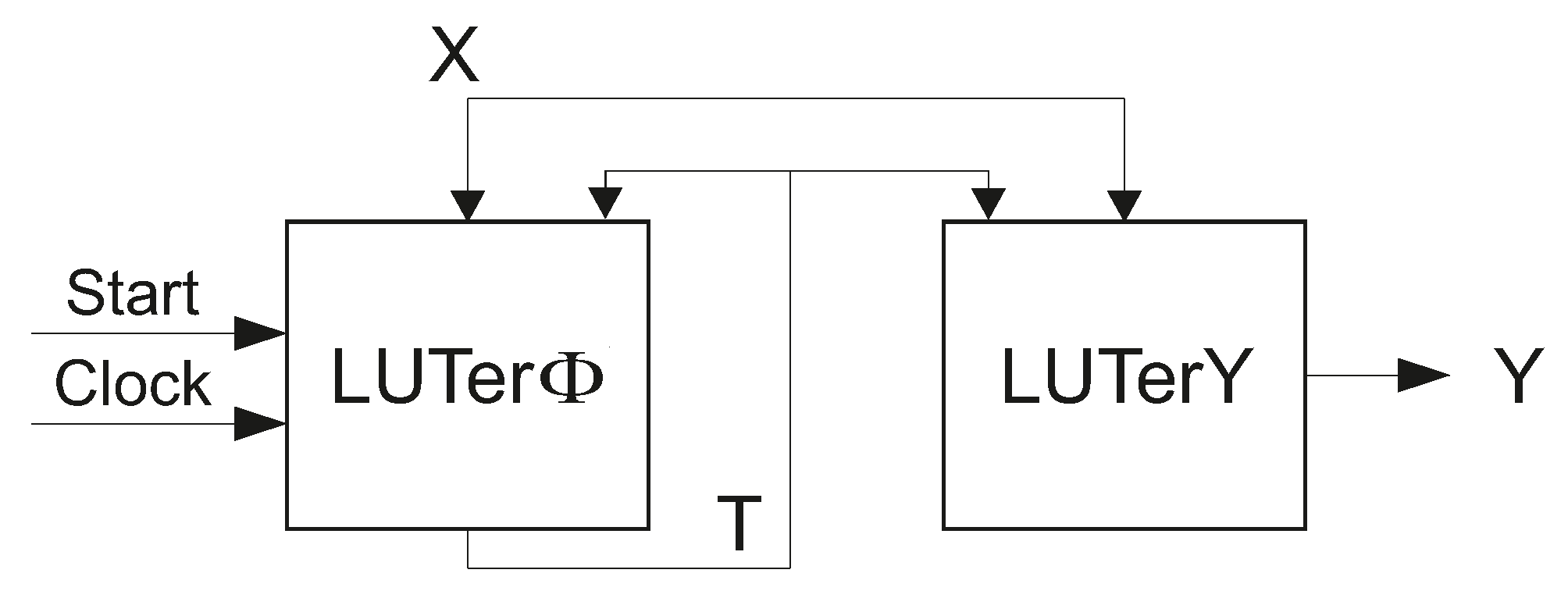
The systems (
2) and (
3) determine a structural diagram of Mealy FSM
(
Figure 1 from [
35]). In
Figure 1, the symbol
denotes a logic block consisting of LUTs.
In the FSM
, the
implements the system (
2), the LUTerY the system (
3). If a function
is generated by a particular LUT, then the LUT’s output is connected with a flip-flop [
9]. The flip-flops form the state register distributed among the LUTs of
. It explains the existence of pulses
Start and
Clock as inputs of
.
The main specific of Mealy FSMs is the dependence of input memory functions and outputs on inputs and state variables. So, these functions have the same nature. This specific can be used to minimize hardware in LUT-based Mealy FSM circuits [
35]. In
Section 4, we will explain how to use this specific.
3. State of the Art
The process of technology mapping is associated with necessity of the solution of some optimization problems [
9,
35]. When designing FPGA-based FSMs, four optimization problems arise [
35]: (1) the reduction of hardware amount, (2) the improvement of performance, (3) the reduction of power consumption, and (4) the improvement of testability. In this article, we propose a way for solution of the first problem.
Denote as
the number of literals [
3] in sum-of-products (SOPs) of functions (
2) and (
3). If the condition
takes place, then it is enough a single LUT to implement a circuit for any function
. If the condition (
4) is violated for some function
, then the corresponding circuit is multi-level. In multi-level circuits, it is quite possible that the same inputs
appear on several logic levels. It results in FSM circuits with the spaghetti-type interconnections.
To improve the circuit characteristics, it is necessary to diminish the number of LUTs and make the system of interconnections more regular. It can be done using the following approaches:
The functional decomposition of functions representing Mealy FSM logic circuits [
8,
17,
19,
20,
24,
36].
The replacement of LUTs by embedded memory blocks (EMBs) [
44,
45,
46,
47,
48,
49,
50,
51].
The structural decomposition of FSM circuits [
35,
43,
52].
The functional decomposition is a very powerful tool used in the process of technology mapping [
19,
53]. If the condition (
4) is violated, then a function is broken down into smaller and smaller components. The process is terminated when any component has no more than
arguments.
If the condition (
4) takes place, then a Mealy FSM logic circuit has exactly R + N LUTs. Otherwise, an FSM circuit is represented by
functions, where
is a set of additional functions different from (
2) and (
3). New functions correspond to components of initial functions obtained in the process of decomposition.
A huge number of methods of functional decomposition are known. Some of them can be found, for example, in [
19,
20,
23]. We do not discuss them in our article. All modern FPGA-based CAD systems include program tools for functional decomposition. These tools can be found in academic systems [
33,
34,
54,
55], as well as in industrial packages [
56,
57,
58]. The open system DEMAIN [
54] includes powerful methods of functional decomposition. Due to this, we chose this system for comparison with our proposed approach.
The optimal state assignment [
9] is a process of obtaining state codes optimizing systems of Boolean functions (
2) and (
3). One of the best academic optimal state assignment algorithms is JEDI distributed with the system SIS [
34]. The JEDI is aimed at reducing the numbers of arguments in functions representing a Mealy FSM logic circuit. In this article, we compare JEDI-based FSMs with FSMs based on our proposed approach
Different state assignment strategies can be found in modern industrial CAD tools. For example, the design tool Vivado [
57] uses the following approaches: the one-hot (
); compact; Gray codes; Johnson codes; speed encoding; automatic state assignment (auto). The same methods can be found in the package XST by Xilinx [
56].
Because modern FPGAs include a lot of flip-flops, the one-hot state assignment is very popular in LUT-based design [
41]. This approach allows producing less complicated combinational parts of FSM circuits than their counterparts based on the binary state encoding where
[
35]. As shown in [
41], if
, then FSMs based on binary state codes have better characteristics than their counterparts based on one-hot codes. The one-hot codes are more preferable if there is
. However, the characteristics of LUT-based FSM circuits significantly depend on the number of inputs [
35]. As it is shown in [
42], if
, then it is better to use one-hot state codes. Otherwise, binary state encoding allows producing better FSM circuits. So, both approaches should be compared with our proposed method. We chose the method Auto of Vivado as a method of binary state encoding. This method allows choosing codes producing FSM circuits with the best possible characteristics.
The main goal of both Gray and Johnson state encoding approaches is the reducing switching activity of an FSM circuit. It allows reducing the dynamic power consumption [
35]. We do not discuss these methods in detail. Such an analysis can be found, for example, in [
42].
So, a large number of state assignment methods are currently known. They are usually focused on optimizing one or more characteristics of FSM circuits. Some of them mostly focus on area reduction. It is very difficult to say which method is the best for a particular FSM. It depends on both the features of FSM and FPGA, as well as on the accepted criteria of FSM circuit optimality.
Each literal of SOP representing a function
corresponds to a wire in the FSM circuit. So, to diminish the number of interconnections, it is necessary to diminish the numbers of literals in Boolean functions (
2) and (
3). The fewer interconnections, the less power is consumed [
28]. Therefore, the optimal state assignment must be performed regardless of whether the condition (
4) is met or not.
Modern FPGAs include a lot of configurable embedded memory blocks [
10,
11,
12]. Replacement of LUTs by EMB allows significantly improve the characteristics of resulting FSM circuits [
41]. Because of it, there are a lot of design methods for EMB-based FSMs [
43,
44,
46,
47,
48,
49,
59]. The survey of different methods of EMB-based design can be found in [
60]. Unfortunately, these methods can be used only if there are “free” EMBs, which are not used to implement other parts of a digital system.
To optimize a LUT-based FSM circuit, it is necessary to eliminate a direct dependence of functions
and
on inputs
. It is a main goal of different methods of a structural decomposition [
35]. To eliminate this dependence, new functions
are introduced to eliminate this dependence. These new functions depend on inputs and/or state variables. To optimize an FSM circuit, the following condition should take place:
Each system of new functions determines a separate block LUTer with its unique input and output variables. These blocks can be viewed as “hardware subroutines” by analogy with subroutines in programming [
61,
62]. If the relation (
5) takes place, then the total number of LUTs implementing functions
is significantly less than their total number in blocks
and
of an equivalent FSM
. Using hardware subroutines allows structuring an FSM circuit. The functions
are used as arguments of functions (
2) and (
3). If the condition
is true, then the total number of LUTs in an FSM circuit is significantly less than it is for an equivalent FSM
.
If (
6) takes place, then the structural decomposition leads to reduced number of literals in SOPs of functions
as compared to initial functions (
2) and (
3). In turn, it reduces the total number of LUTs in blocks
and
(as compared to
). If condition (
4) is violated for some functions
, then the methods of functional and structural decomposition should be used together in the process of technology mapping. A survey of different methods of structural decomposition can be found in [
35].
In this article, we discuss two methods of structural decomposition. They are the methods of replacement of inputs and encoding of outputs. They have been proposed to minimize the control memory size in microprogram control units (MCU) [
63]. Next, they were applied in PLA-based FSMs [
64]. Each of these methods was used separately in EMB-based FSM design [
44,
45,
48,
60]. However, they have never been used in LUT-based FSM design. In this article, we propose to combine these methods together to optimize characteristics of LUT-based Mealy FSMs.
The first method is a replacement of inputs
by additional variables
where
[
64]. To do it, it is necessary to create an SBF
In MCUs, SBF (
7) is implemented using a multiplexer. The additional variables are used as arguments of functions
. These functions are represented as
The functions (
8) and (
9) have a regular nature [
35]. So, they can be implemented as a memory block having
address inputs and
outputs.
Using this approach leads to FSM
shown in
Figure 2. It includes a multiplexer implementing SBF (
7) and a memory block implementing systems (
8) and (
9).
In the classical MCU [
63], only a single input is checked in each cycle of operation (
). This results in rather slow control units. To decrease the number of cycles required for implementing a control algorithm, it is necessary to increase the value of
G. To optimize an MCU performance, the value of G is determined as [
64]:
In (
10), the symbol
stands for the set of inputs determining transitions from the state
.
The model
was used in the FPGA-based design. Different
-based approaches are discussed, for example, in [
60]. In all discussed cases, EMBs implement systems (
8) and (
9). The system (
7) is implemented with LUTs.
Collections of outputs (COs)
are generated during interstate transitions. The minimum number of bits in the code
is determined as
To encode COs by codes , some additional variables are used.
If COs are encoded, then the system of outputs is represented as
In the case of MCU, the system (
12) is implemented using two blocks, namely, a decoder and a coder [
35].
To generate the additional variables
, it is necessary to find an SBF
In the case of MCU, both systems (
13) and (
2) are implemented by a memory block. In the case of FPGA-based design, a memory block is represented as a network of EMBs.
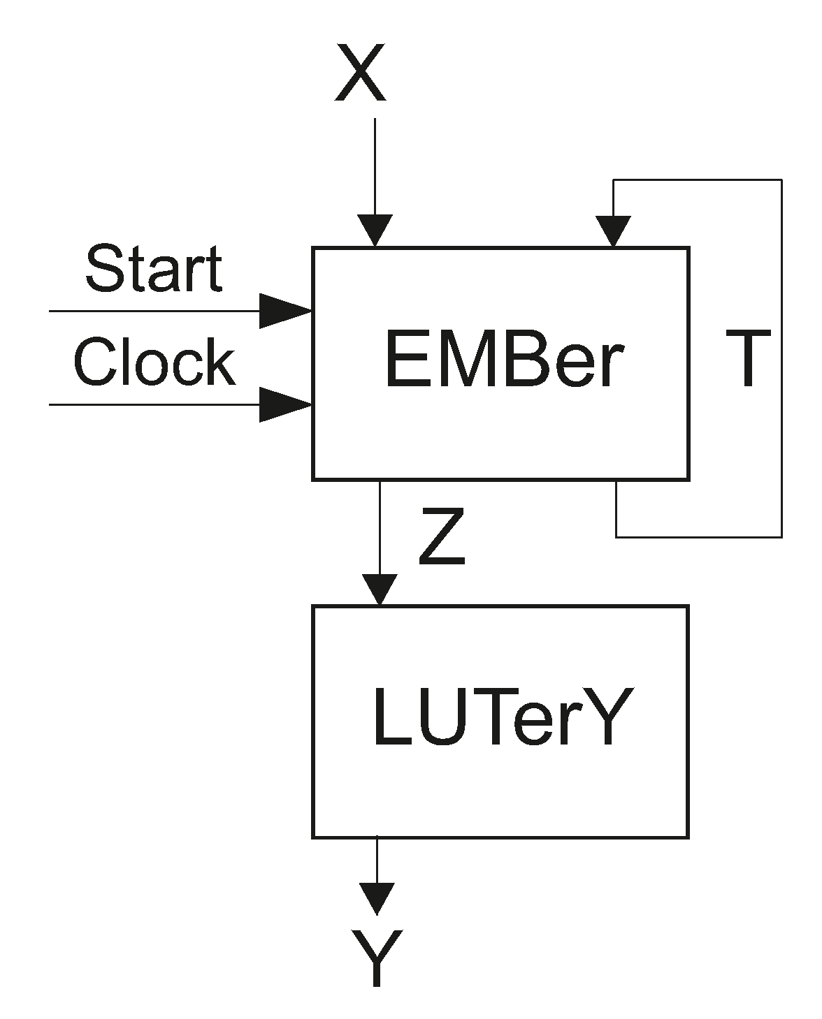
Using the encoding of COs in FPGA-based design leads to Mealy FSM
shown in
Figure 3.
In FSM
, the block EMBer implements systems (
2) and (
13). The block LUTer implements the system (
12).
So far, these methods have been used separately to improve characteristics of circuits of FPGA-based FSMs. Moreover, some parts of FSM circuits have been implemented using EMBs [
45,
47]. In this article, we propose to use these methods together. Moreover, all functions are implemented by LUTs. This approach leads to Mealy FSM logic circuits having three levels of logic. The circuit for each level of logic can be viewed as a hardware subroutine. This approach allows structuring a resulting FSM circuit and makes the system of interconnections more regular. We denote the proposed Mealy FSM by the symbol
.
4. Main Idea of the Proposed Method
Consider some Mealy FSM represented by an STT. We assume that the following procedures have been executed: (1) the replacement of inputs; (2) the encoding of COs; (3) the encoding of states and (4) the transformation of initial STT into the DST of FSM . To get SBFs representing , we should transform the DST of FSM into a DST of Mealy FSM .
To obtain the arguments of functions (
8) and
, it is necessary to replace the column
of the DST of FSM
by the column
. It is executed in the following way: if an additional variable
replaces an input
for a state
, then the variable
(or its negation) from the column
is replaced by the variable
(or its negation) in the column
for all transitions from the state
.
To obtain functions , it is necessary to replace the column of the DST of FSM by the column . The filling of the column is executed in the following manner. If the h-th row of DST includes a CO such that the r-th bit of is equal to 1, then the symbol should be written in the h-th row of the column of DST of FSM .
Using a DST of FSM
, we can derive the systems (
8) and
Using the table of replacement of inputs, we can get the system (
7). Next, using the content of collections of outputs, we can obtain the system (
12).
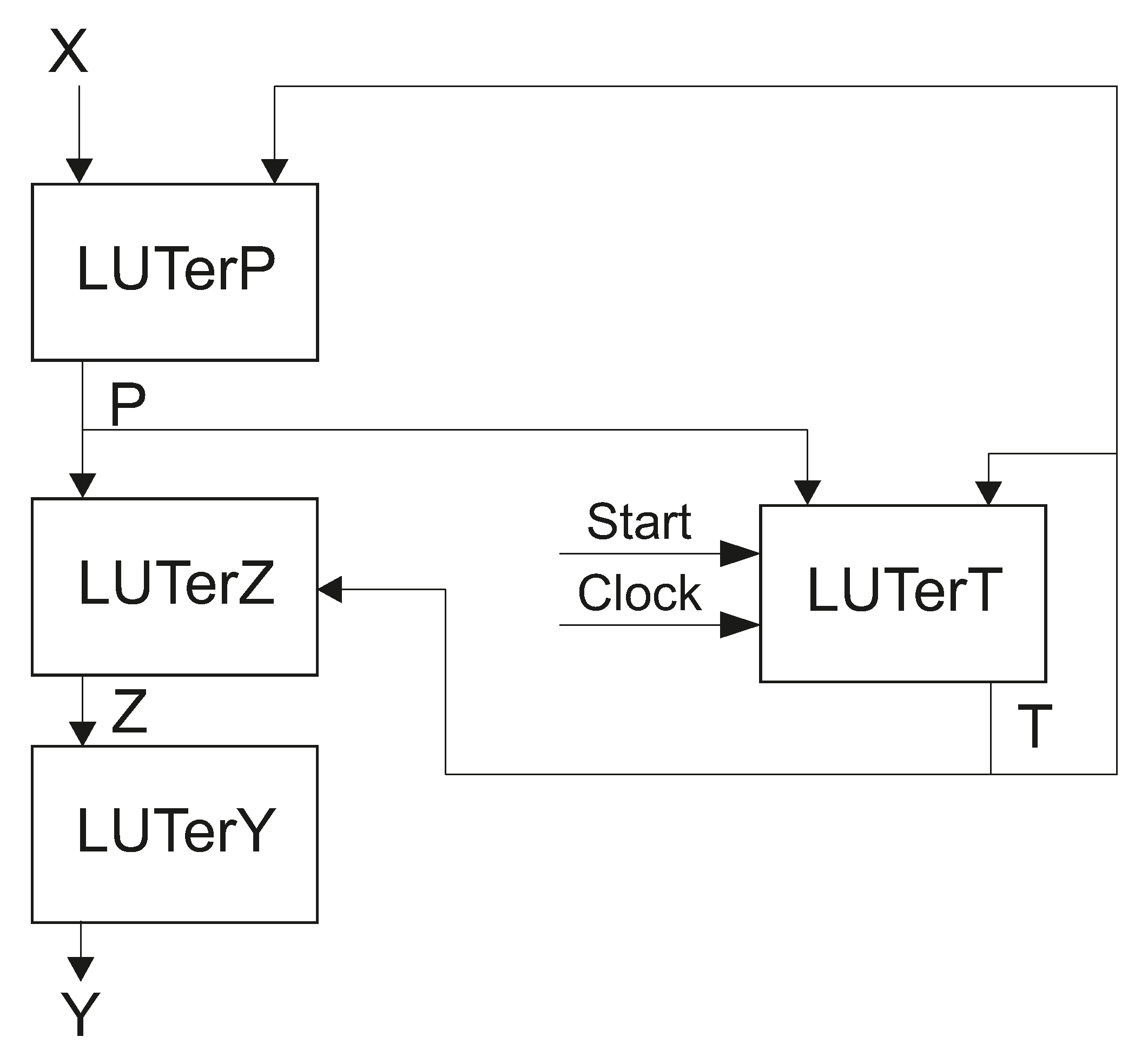
Until now, the methods of replacement of inputs and encoding of the collections of outputs were used separately in EMB-based Mealy FSM design. In this article, we propose to use them together in LUT-based Mealy FSMs. There are three levels of logic blocks in the proposed Mealy FSM
. Its structural diagram is shown in
Figure 4.
In FSM
, the first level of logic is represented by a block
, the second level includes blocks
and
, the third level includes a block
. The blocks implement the following SBFs: the
implements the system (
7), the
the system (
14), the
the system (
8), and the
the system (
12).
If the condition
takes place, then the
consists of
LUTs and
of
R LUTs. It is the best possible case. If the condition (
15) is violated, then it is necessary to apply the methods of functional decomposition for some functions from SBFs (
8) and (
14).
If the condition
takes place, then there are exactly
N LUTs in the circuit of the
. If this condition is violated, then it is necessary to apply the methods of functional decomposition for some functions from SBF (
12).
In this article, we propose a design method for Mealy FSM . We assume that an FSM is represented by an STT. The method includes the following steps:
Executing the replacement of inputs by additional variables .
Executing the state assignment in a way optimizing the SBF .
Deriving the collections of outputs from the STT.
Executing the encoding of COs in a way optimizing the SBF .
Creating the DST of FSM on the base of initial STT.
Deriving the SBFs (
7), (
8), (
12) and (
14) from the DST.
Implementing circuit of FSM using particular LUTs.
Some steps of the proposed method are connected with solution of optimization problems. We discuss these problems in the following Section.
5. Example of Synthesis
If a Mealy FSM is synthesized using a model , then we denote it by the symbol . Consider an example of synthesis for Mealy FSM . An FSM circuit will be implemented using LUTs with .
Executing the replacement of inputs. We start from constructing sets
. A set
includes inputs
determining transitions from the state
. Using
Table 1 gives the following sets:
,
,
,
,
and
.
Using (
10) gives
. So, there is the set
. Using (
1) gives the number of state variables
.
We should construct a table of replacement of inputs [
35]. This table has
M columns marked by states
and
G rows marked by variables
. If an input
is replaced by a variable
in the state
, then there is the symbol
written at the intersection of the column
and the row
[
64].
Inputs
written in a row
form a set
. If
, then the circuit generating
is implemented as a single LUT. In the discussed case, there is
. To optimize the circuit of
, we should distribute inputs
in a way providing the relation
(
). It could be done using the approach from [
64]. One of the possible solutions is shown in
Table 2.
Executing the state assignment. To optimize the circuit of
, it is necessary to diminish the number of literals in functions (
7) [
64]. It can be done due to a proper state assignment. These methods are based on results of the work [
64].
Using (
1) gives
. So, there are the sets
and
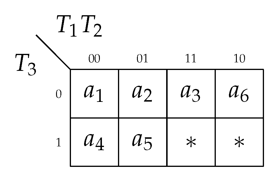
. One of the possible outcomes of the state assignment is shown in
Figure 5.
Deriving the collections of outputs. This step is executed in the trivial way. The collections
are written in the column
of an STT. Using
Table 1, the following COs can be found:
,
,
,
,
,
,
,
,
and
.
To optimize the circuit of LUTerY, it is necessary to minimize the number of literals in functions (
12). Furthermore, it allows minimizing the number of interconnections between the blocks
and
.
Executing the encoding of COs. We start this process from a system representing outputs
. as functions of collections
. It is the following system in the discussed case:
There are
collections of outputs in the discussed case. Using (
11) gives
and
. Using the method [
64] allows obtaining codes of COs shown in
Figure 6.
Creating the DST of FSM
. Having codes of states and COs, we can transform the initial STT (
Table 1) into a DST of Mealy FSM
(
Table 3).
Consider the row
of
Table 3. There is
and
. As follows from
Figure 5, the code of
is equal to 010. Due to it, there is the symbol
in the column
. There is the symbol
in the row 1 of STT. As follows from
Table 2, the input
is replaced by the variable
for the state
. Due to it, there is the symbol
in the first row of DST (
Table 3). There is the collection of outputs
in the first row of
Table 1. As follows from
Figure 6, there is
. Due to it, there is the symbol
in the row 1 of DST (
Table 3). All other rows of
Table 3 are filled in the same way.
Deriving SBFs representing the circuit of
. During this step, the functions (
7), (
8), (
12) and (
14) should be found. It can be done using
Table 2 and
Table 3, as well as codes from Karnaugh maps shown in
Figure 5 and
Figure 6.
We start from the SBF (
7). We use the symbol
to denote a conjunction of state variables (or their complements) corresponding to the code
.
The following system can be derived from
Table 2:
Using codes from
Figure 5, we can get the following minimized functions:
In the discussed case, the system (
19) represents
. Each equation of (
19) includes not more than six literals. Because
, there are only
LUTs in the circuit of
.
Each row of DST of FSM
corresponds to the product term
In (
20), the symbol
denotes a conjuction of variables
(or their compliments) written in the column
of DST.
The functions (
8) and (
14) depend on terms (
20). For example, the following equations can be derived from
Table 3:
All other functions and are constructed in the same manner.
In the discussed case, there is . Because , the condition takes place for any function . It means that there are R=3 LUTs in the circuit of and LUTs in the circuit of .
Using system (
17) and codes from
Figure 6, we can get the following system:
The analysis of (
23) shows that there is no need in a LUT to implement the function
. Because
is less than
, the condition (
16) takes place. So, it is necessary
LUTs to implement
.
In general case, each function from (
12) has
literals. For N functions, it gives
literals. In the discussed case, there is
literals. Each literal corresponds to the interconnection between blocks
and
. As follows from (
23), there are 16 literals in this system. It gives a 42% savings in the number of interconnections compared to the general case. This economy is achieved due to chosen encoding of COs
. It should give economy in the power consumption.
So, there are LUTs in , LUTs in , LUTs in , and LUTs in . It gives 16 LUTs in the logic circuit of Mealy FSM .
The last step of design is connected with the placement and routing procedures [
16]. It is executed using industrial CAD tools such as, for example, Vivado by Xilinx [
57]. We do not discuss this step for a given example.
It is known that any sequential block can be represented using either model of Mealy FSM or Moore FSM [
3]. There is the following specific of Moore FSM: its outputs depend only on states. It means that, for Moore FSMs, state codes can be viewed as the codes of collections of outputs. So, there is no sense in using additional variables encoding the collections of outputs. It means that the proposed approach can be used only in the case of LUT-based Mealy FSMs.
6. Experimental Results
To investigate the efficiency of proposed method, we use standard benchmarks from the library [
29]. The library includes 48 benchmarks taken from the design practice. The benchmarks are rather simple, but they are very often used by different researches to compare new and known results [
9,
43]. The benchmarks are represented in KISS2 format. These benchmarks are Mealy FSMs, so we can directly use them in our research. The characteristics of these benchmark FSMs are shown in
Table 4.
The process of obtaining synthesis research results in Vivado [
57] has been divided into two stages. The first stage was a generation of the VHDL code based on benchmarks saved in the KISS2 format. Each benchmark was generated by the tool K2F [
35,
45] according to the given FSM model. It should be noted that generated code uses a specific Vivado code style [
65] in order to provide the proper FSM extraction and fully synthesizable code. Then, in the next stage, the VHDL code was imported into Vivado (ver. 2019.1). The target device was the Xilinx Virtex 7 (XC7VX690TFFG1761) [
66]. The chip includes LUTs with six inputs. The synthesis and optimization options were set to:
max_bram 0, opt_design -retarget -propconst -bram_power_opt and the selected FSM state encoding method one of the following:
auto, one_hot, sequential, johnson or
gray. The final results presented in the tables are taken after the post-implementation.
As we have found, our method can give economy in area if . We have divided the benchmarks into categories using the values of and . If , then benchmarks belong to category 0 (trivial FSMs); if , then to category 1 (simple FSMs); if , then to category 2 (average FSMs); if , then to category 3 (big FSMs); otherwise, they belong to category 4 (very big FSMs). Obviously, there is no sense to apply our approach to FSMs belonging to category 0. As our researches show, the higher the category, the more saving the proposed approach gives.
Four other methods were taken to compare with our approach. They are: (1) Auto of Vivado; (2) One-hot of Vivado; (3) JEDI-based FSMs and (4) DEMAIN-based FSMs. The results of experiments are shown in
Table 5 (the number of LUTs) and
Table 6 (the operating frequency).
Table 5 and
Table 6 are organized in the same order. The rows are marked by the names of benchmarks, the columns by design methods. The rows “Total” include results of summation for corresponding values. The summarized characteristics of our approach (
—based FSMs) are taken as 100%. The rows “Percentage” show the percentage of summarized characteristics of FSM circuits implemented by other methods respectively to benchmarks based on our approach. Let us point out that the model
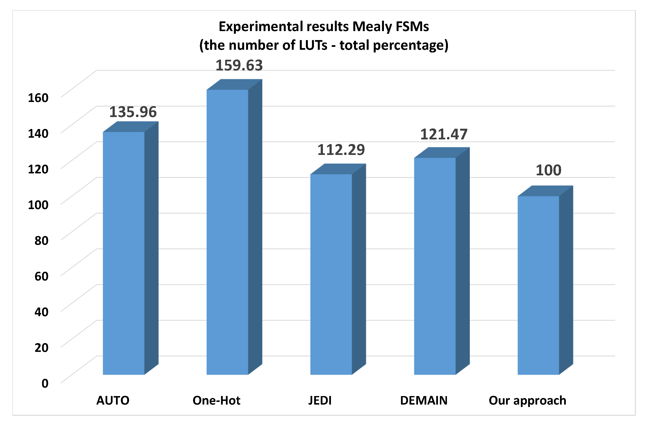
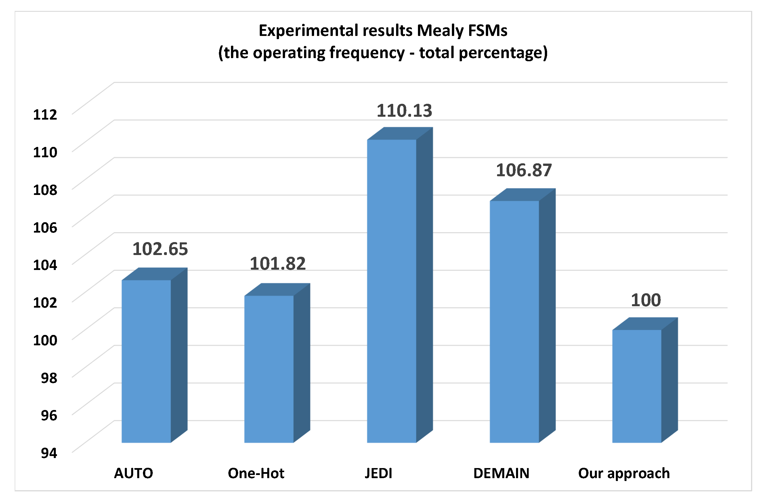
is used for designs with Auto, One-hot, JEDI and DEMAIN. Furthermore, for better visualization, summary data are presented in the
Figure 7,
Figure 8 and
Figure 9.
As follows from
Table 5 and
Figure 7, the
—based FSMs required fewer LUTs than it is for other investigated methods. There is the following economy: (1) 35.65% regarding Auto; (2) 59.27% regarding One-hot; (3) 12.04% regarding JEDI-based FSMs and (4) 21.20% regarding DEMAIN-based FSMs. The higher is the category, the greater is the gain in LUTs. For trivial and simple FSMs, the better results are produced by either JEDI or DEMAIN. The gain are becoming more and more noticeable, starting from the average FSMs.
As follows from
Table 6 and
Figure 8, the
—based FSMs have a lower operating frequency than it is for other investigated methods. There is the following loss: (1) 2.65% regarding Auto; (2) 1.82% regarding One-hot; (3) 10.13% regarding JEDI-based FSMs and (4) 6.87% regarding DEMAIN-based FSMs. However, starting from big FSMs, the losses are getting smaller. It is connected with the fact that
—based FSMs always have three levels of logic and more regular system of interconnections.
The main goal of the proposed approach is to reduce the LUT count in circuits of FPGA-based Mealy FSMs. As follows from
Table 5, the degree of reduction in the number of LUTs depends on the category of an FSM. To clarify this dependence, we have created
Table 7 (experimental results for category 0),
Table 8 (experimental results for category 1) and
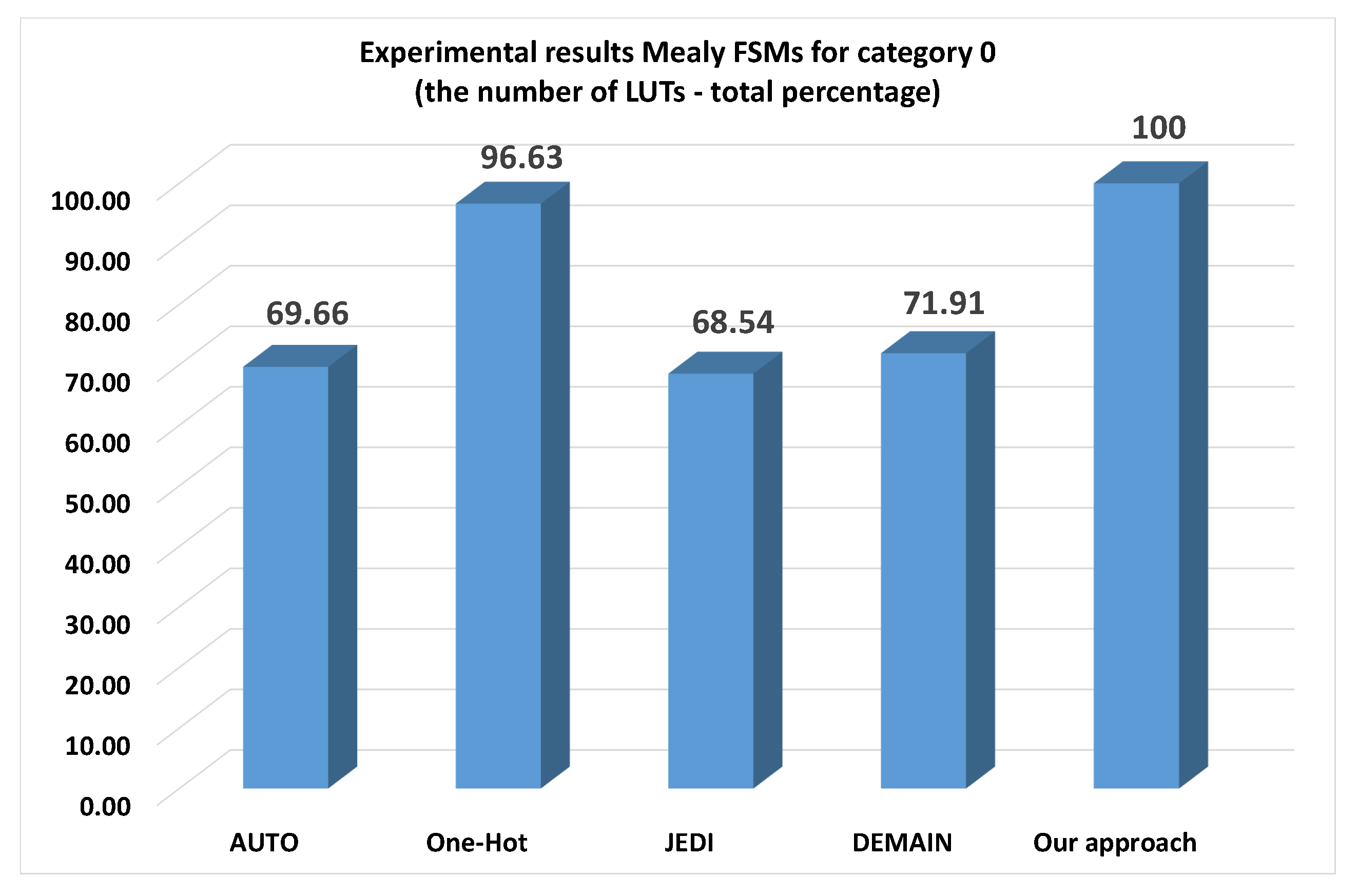
Table 9 (experimental results for categories 2–94). Furthermore, we present these results by graphs on
Figure 9,
Figure 10 and
Figure 11, respectively.
As follows from
Table 7 and
Figure 9, the proposed method produces FSM circuits having more LUTs than it is for other investigated methods. Our method has the following loss: (1) 30.34% regarding Auto; (2) 3.37% regarding One-hot; (3) 31.46% regarding JEDI-based FSMs and (4) 28.09% regarding DEMAIN-based FSMs. So, there is no sense in using our approach for designing trivial FSMs. However, it gives an economy in LUTs starting from simple FSMs (category 1).
As follows from
Table 8 and
Figure 10, the
—based FSMs of category 1 required fewer LUTs than it is for other methods. There is the following economy: (1) 23.03% regarding Auto; (2) 65.52% regarding One-hot; (3) 3.47% regarding JEDI-based FSMs and (4) 12.62% regarding DEMAIN-based FSMs. So, for the category 1, our approach produces FSM circuits slightly better than JEDI-based FSMs.
Our method produces best results for FSMs from categories 29-4 (
Table 9 and
Figure 11). It is very interesting that the gain respectively the one-hot approach is approximately the same as it is in the previous case. However, we provide a bigger gain for other investigated methods as compared to FSMs of the category 1. There is the following economy: (1) 46.93% regarding Auto; (2) 19.63% regarding JEDI-based FSMs and (3) 29.39% regarding DEMAIN-based FSMs. So, our approach produces FSM circuits with better amount of LUTs for Mealy FSMs having
.
Till now, we compared our approach with
-based FSMs. However, we also compared the
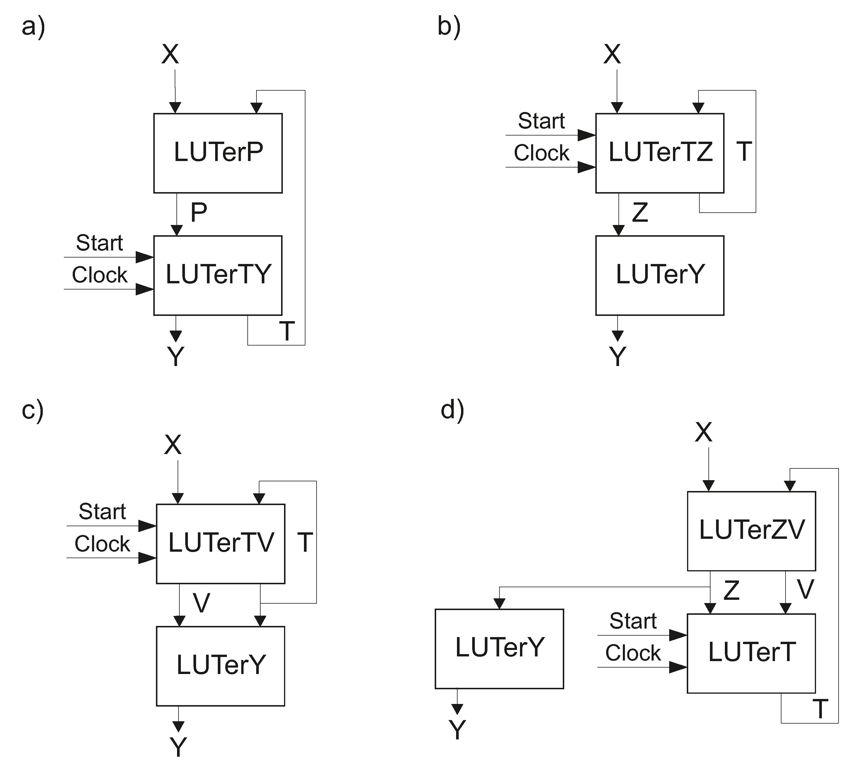
-based FSMs with FSMs having two levels of logic. The structural diagrams of these FSMs are shown in
Figure 12. The FSM
is based on the replacement of inputs (
Figure 12a). There is no such an FSM in the known literature. We have got its structural diagram by transformation the FSM
(
Figure 2). We replaced the multiplexer by the block
; the memory block is replaced by
. The
implements the system (
5), the LUTerTY the systems (
6) and (
7).
The FSM
is based on the encoding of collections of outputs (
Figure 12b). There is no such an FSM in the known literature. We have got its structural diagram by transformation the FSM
(
Figure 3). We replaced the block
by the block
generating functions (
2) and (
11). As it is for FSM
, the
implements the system (
10).
The FSM
is based on the transformation of state codes into outputs (
Figure 12c) [
35]. In this FSM, additional variables from the set
V replace inputs for output functions. The FSM
is based on the transformation of collections of outputs into state codes (
Figure 12d) [
35]. In this FSM, additional variables from the set V replace inputs for input memory functions. Both methods belong to the group of object transformation methods [
35]. We do not discuss these approaches in this article. We just use them as examples of FSMs having two levels of logic.
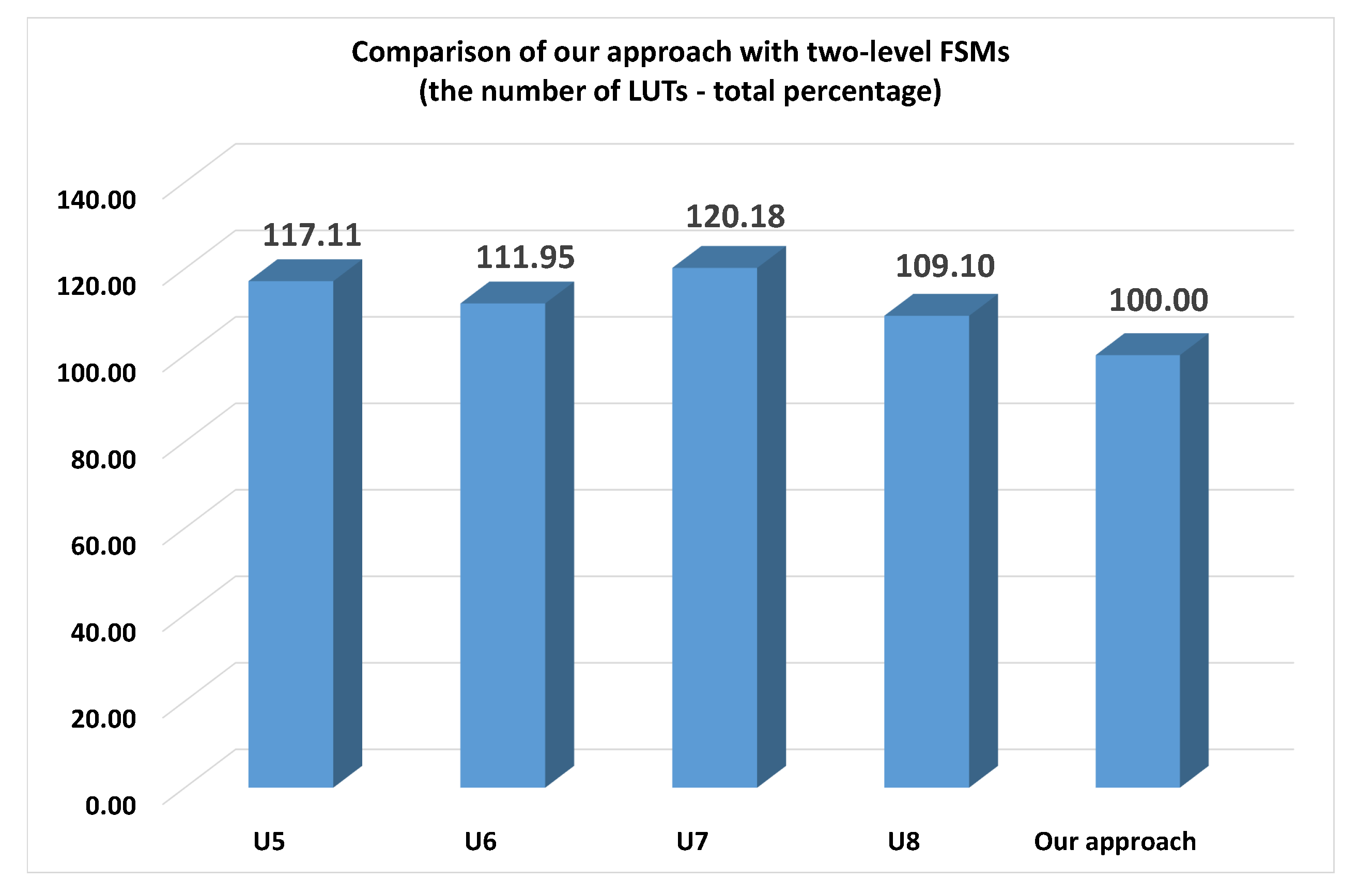
We compared the FSMs (
Figure 12) with our approach for the most complex benchmarks (categories 2–4). The results of experiments are shown in
Table 10 and
Figure 13. As follows from
Table 10, our method produces better results for FSMs than it is for FSMs
-
. There is the following economy: (1) 17.11% regarding
; (2) 11.95%
(3) 20.18% regarding
and 4) 9.1% regarding
. So, our approach produces FSM circuits with better amount than two-level Mealy FSMs having
. However, the gain is noticeably less than for
-based FSMs from these categories.
So, the results of our experiments show that the proposed approach can reduce the LUT counts respectively to single- and two-level Mealy FSMs having
. Of course, this conclusion is true only for benchmarks [
27] and the device XC7VX690tffg1761-2 by Virtex-7, where LUTs have 6 inputs. It is almost impossible to make a similar conclusion for the general case. However, we hope that our approach rather good potential and can be used in CAD systems targeting FPGA-based Mealy FSMs.
