Article

Multiple-Loop Control Design for a Single-Stage PV-Fed Grid-Tied Differential Boost Inverter

1
Department of Electronics, Electrical Engineering and Automatic Control, Universitat Rovira i Virgili, 43007 Tarragona, Spain
2
Electrical Engineering Department, King Saud University, Riyadh 11451, Saudi Arabia
3
School of Electrical Engineering, Wuhan University, Wuhan 430072, China
*
Author to whom correspondence should be addressed.
Appl. Sci. 2020, 10(14), 4808; https://doi.org/10.3390/app10144808
Submission received: 23 June 2020 / Revised: 7 July 2020 / Accepted: 8 July 2020 / Published: 13 July 2020
(This article belongs to the Special Issue Advancing Grid-Connected Renewable Generation Systems 2019)

Abstract

:
This paper focuses on the control design of a differential boost inverter when used in single-stage grid-tied PV systems. The inverter performs both Maximum Power Point Tracking (MPPT) at the DC side and Power Factor Correction at the AC side. At first, the state-space time-domain averaged model of the inverter is derived and the small signal frequency domain model is obtained using a quasi-static approximation in which the inverter is treated as a DC–DC converter with a slowly varying output voltage. Then, the controllers are designed using a three-loop strategy in which the inverter inductor currents loop is used for suitable compensation, the DC Photovoltaic (PV) voltage loop is used for MPPT and the output grid current loop is used for Power Factor Correction (PFC) and active power control. The selection of the control parameters is based on a compromise among suitable system performances such as settling time of the input PV voltage, the sampling period of the MPPT, total harmonic distortion of the output grid current, power factor as well as suppression of subharmonic oscillation for all the range of the operating duty cycle. The resulting design ensures that the oscillations of the voltage, current and power at the DC side and the grid current at the AC side are effectively controlled. The validity of the proposed control design is verified by numerical simulations performed on the switched model of the system demonstrating its robustness and fast response under irradiance variations and MPPT perturbations despite the nonlinearity and complexity of the system.

1. Introduction

The increasing demand for the use of electrical energy, taking place in the recent years, has led to serious concerns about sustainability and the related environmental issues. Consequently, a great attention is being given to the production of electrical energy using renewable energy resources such as photovoltaic (PV) generators and wind turbines due to their abundance and almost zero environmental impacts [1]. Therefore, distributed renewable generation of electricity both in small-scale and large-scale power systems is gaining much interest in the recent years. In particular, PV energy has been wide spread during the last ten years due to the reduction in the cost of PV modules, increase of their efficiency and easy maintenance [2,3]. Although the basic PV system principles and elements remain the same, three main types of of PV systems can be distinguished: stand-alone, grid-connected, and hybrid. Grid-connected PV systems account for more than 99% of the PV-installed capacity compared to stand-alone systems [4]. Grid connection of PV systems requires a highly efficient inverter which is considered the main element in PV installations.
Grid-connected PV systems can be built by using either two-stage or single-stage approaches. In the two-stage approach an intermediate DC–DC power stage is inserted between the PV module and the DC–AC grid-tied inverter [5,6,7]. This intermediate stage is responsible for decoupling the PV system operating point from the PV inverter grid control by enabling a suitable average voltage at the inverter DC side. In two-stage grid-connected PV systems, each stage has its independent task and the control design is relatively simple for each stage. The single-stage grid-connected PV system consists of a PV generator, a DC-link capacitor and DC–AC inverter used both to extract the maximum power from the PV generator and to inject a sinusoidal current into the grid with near unity power factor [8,9].
In conventional PV systems, a single inverter, called a central inverter, is connected with several PV panels and if a partial shading takes place, the efficiency of the entire PV field is degraded. This main disadvantage of central inverters is overcome by using microinverters that are suitable for small-scale residential uses where each PV module is connected to an inverter separately forming an AC module with its own Maximum Power Point Tracking MPPT control. Therefore, the total harvested power increases under a partial shadowing condition since the power of each PV panel is controlled independently and separately from the others. Moreover, single-stage microinverters are connected to the AC side directly, hence eliminating the DC cable losses and therefore improving further the system efficiency.
Voltage step-down DC–AC inverters based on H-bridge topology are conventionally used to connect a PV system to the grid generating a sinusoidal output voltage for supplying an AC load. These kinds of inverters are conventionally preferred because they have inherent control-to-output linearity in large-signal sense. Nevertheless, in these kinds of inverters, the maximum output voltage at the AC side must be always smaller than the DC voltage. Therefore, in single-stage cases based on voltage source H-bridge topology, many strings of PV panels are connected in series to increase the output voltage [10].
The efficiency of the two-stage system is negatively affected by using increased component count and switching devices. Moreover, the size and the cost are higher compared to single-stage grid-connected PV systems. The low reliability is another shortcoming of the two-stage approach. To reduce the overall cost and complexity, single-stage structures can be used.
Single-stage grid-connected DC–AC conversion systems with boosting voltage capability has recently attracted the attention of many researchers. Single-stage structures of microinverters not only perform DC–AC conversion but also perform voltage boosting. Moreover, differential inverter topologies seem to prevail in price and size due to the utilization of small passive elements of DC–DC converters hence improving the efficiency [11].
Some inverter topologies with voltage boosting capability such as the Z-source inverter [12] and the quasi-Z-source inverters [13,14] have been also developed. Another topology with voltage boosting capability is the DC–AC differential boost inverter that has been presented in [15]. This topology was obtained by connecting the load differentially across two identical DC–DC boost converters sharing the same input. The same concept can be applied to any DC–DC converter to form a differential inverter. A study of boost, buck, buck-boost and Ćuk differential inverters has been presented in [16]. The differential boost inverter has been used for power processing stage fuel-cell energy system [17,18]. It has been also used for high quality sine wave generation with a high oscillation frequency [19] where a dynamic modulator has been adopted to control the capacitor voltage of the boost inverter.
Since its introduction in [15], many control strategies have been applied to the differential boost inverter. The nonlinear control-to-output behavior in large-signal dynamic sense and the non-minimum phase nature in the small-signal sense of the boost inverter make the direct tracking of the sinusoidal voltage reference in this kind of topologies a difficult task [20]. Sliding mode control was first applied in which a switching surface composed by weighted errors in the output capacitor voltages and the inductor currents is used [15]. The inverter model with a constant voltage source and a resistive load system and its controller design has been addressed in [21] using a sliding mode control of the inner current loop and a PI controller for the AC output voltage. Adaptive control for the boost inverter has been designed in [22] where by using energy shaping methodology with a suitable Hamiltonian function an autonomous oscillator is generated without an external reference signal hence being the approach suitable for resistive loads.
Other Pulse Width Modulation (PWM) techniques, mostly based on two-loop linear control scheme, have been used with a slow outer loop for the capacitor voltages and a fast inner loop for inductor currents. Two separate control loops are usually used for each converter. Examples of this control strategy can be found in [17,20]. Most of the previous studies reported on the differential boost inverters have been tested by a resistive load. Grid-connected boost inverter was also considered in [23,24] for integrating energy storage devices such as a battery, fuel cell or supercapacitor to a single-phase AC grid. A load-adaptation mechanism for the boost inverter has been carried out to design a state observer for some of the converter variables in order to estimate the load [22] leading to a fast system response and successful adaptation of the load parameter as confirmed by numerical simulations in the same paper. A current control strategy with zero steady-state tracking error has been applied to a differential grid-connected boost inverter supplied from an ideal input voltage source [25]. In that work, based on the internal model principle, Proportional-Resonant (PR) controllers instead of Proportional-Integral (PI) controllers were used to achieve zero phase and amplitude tracking error demonstrating experimentally that the proposed control meet grid-connection harmonics standards. The grid-connection of the differential boost inverter and the use of PR controller for the grid current loop was also addressed in [26] where a sliding mode control for the inner inductor current loop and a PI controller was used.
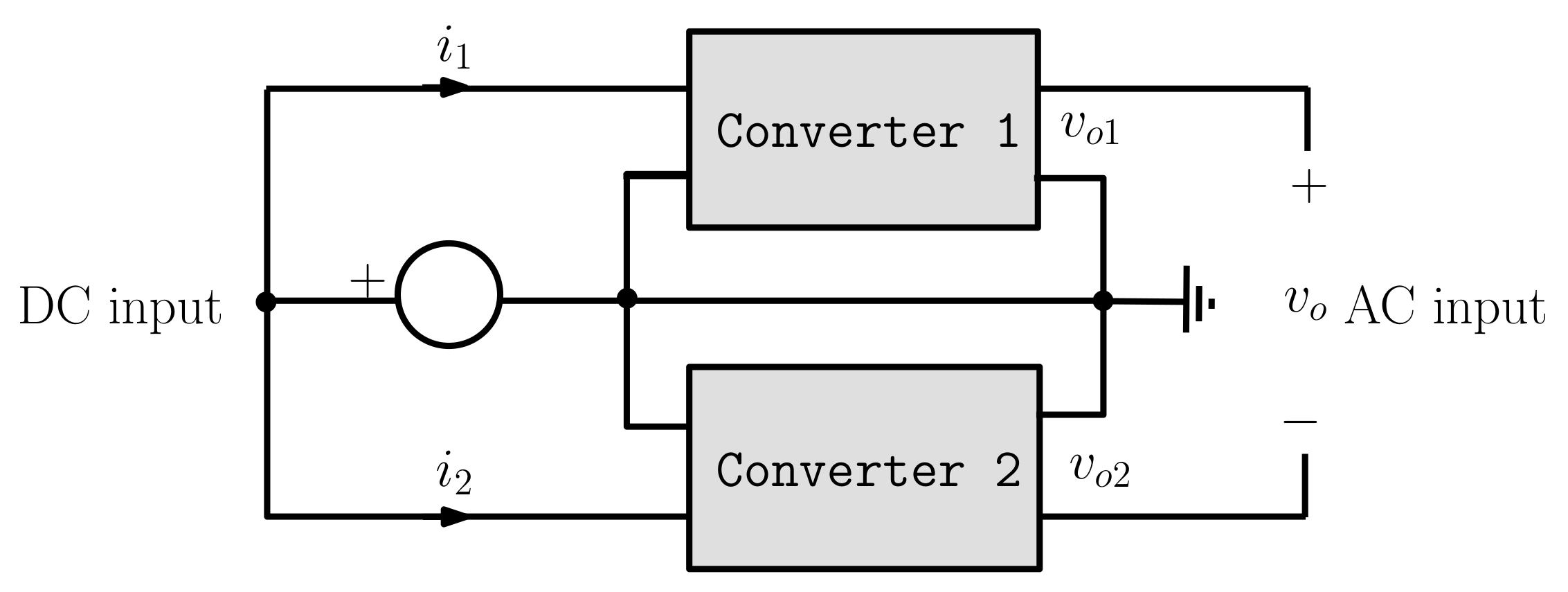
In most of the published works, a decoupling between the two branches of the differential inverter is performed with the aim to simplify the control design. Using such an approach, the inverter is not taken as a whole system but two identical decoupled converters and the output of each branch is controlled individually and separately from the other branch. The control of the inverter is performed by controlling each DC–DC boost converter separately. In this approach, each boost converter is controlled to generate a DC biased sinusoidal voltage with a phase shift of 180 ° such that the difference between both output voltages is an AC sine wave signal that is used to supply the AC load. The DC–DC boost converter cannot generate a voltage lower than its DC input voltage, the DC component of the voltage generated by each DC–DC boost converter must be larger than the DC input voltage. For that, two controllers for each loop and two modulators are used for the entire system. Hence increasing the number of components in the control system. Moreover, the two branches of the inverter are coupled both at the input and the output sides. In particular, in PV application, the input side is no more a constant voltage but a state variable that is coupled to both branches of the inverter. Model predictive control was applied to the differential boost inverter in [27] used for PV grid-connected system applications where it was demonstrated by numerical simulations that a simple control comparable to classical control techniques can be used.
Most of the previous works have converted the problem of controlling the boost inverter to the problem of controlling two identical DC–DC boost converters. An exception where the inverter was controlled as an individual system is [28] where a strategy for generating a sinusoidal voltage at the output of the inverter with resistive load directly from the difference between the capacitor voltages of both converters. The approach was finally implemented by a fixed frequency PWM approach based on a sliding mode control theory leading to a robust system under load and input voltage variations with simple implementation. One advantage of controlling the system as whole is a decrease in the number of required sensors and simplicity of the control scheme to be implemented. Sliding mode control has many advantages for nonlinear systems. Nevertheless, the main drawback of the sliding mode control in power electronics field is that it is ultimately implemented by using hysteretic comparators leading to variable switching frequency.
PR controllers have been used to overcome the issues related to the use of PI control in single-phase inverters [11,29]. Nevertheless, since the AC signals are much slower than the switching frequency, conventional controllers can still be used as will be shown in this paper. However, PI controllers can lead to steady-state errors and phase shifts when used to control sinusoidal signals. The bandwidth must be enough large but high bandwidth could lead to either instability due to the phase lag introduced by the PI controller. Therefore, a phase boosting is needed near the desired crossover frequency and this can be accomplished by using type III controllers widely adopted in the control of DC–DC converters [30]. In most of the published works, resistive passive loads and constant input voltage were considered. Except [21], real nonlinear real PV sources and grid connection have not been fully addressed for the differential boost inverter due particularly to its complexity when it is used in PV systems such as in grid-connected microinverter applications where the cost and the simplicity are to be taken into account.
When the system is supplied by a constant input voltage and loaded by a resistive load, its design can be roughly divided in the design of two identical boost converters resulting eventually to order reduction of the overall dynamics. In the case of a PV-fed grid connected inverter and due to the coupling between the two converters at the DC side by dynamics of the PV generator voltage and at the AC side by the dynamics of the grid current, such an approach cannot be applied and the differential inverter must be treated a whole system.
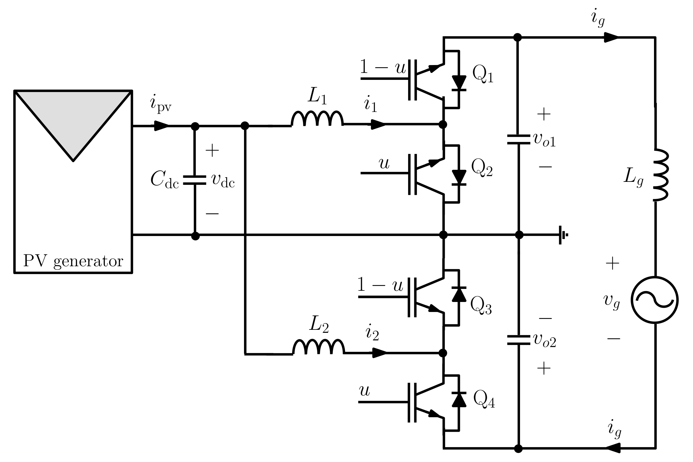
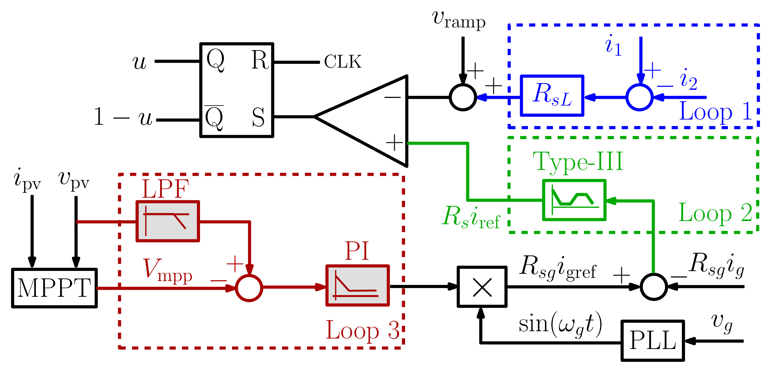
The main contributions of this work are the derivation of a control-oriented model and the design of a three control loop strategy for a PV-fed grid-tied boost inverter as whole system without any decoupling between the two inverters hence dealing with its full-order model. The strategy is based on peak current mode control for the fast inner loop, a type III compensator for the grid current loop and a PI regulator with a pre-filter for the DC PV voltage loop. The main concern is the design of the three control loops for the inverter supplied from a series strings of PV panels and connected to the AC grid performing both Maximum Power Point Tracking (MPPT) at the DC side and Power Factor Correction (PFC) control at the AC side. For that, the study starts with a suitable mathematical modeling of the inverter. The design of its different control loops is carried out using simple approaches widely adopted for DC–DC converters while resulting in excellent system performances. At first, the state-space time-domain averaged model of the inverter is derived and the small signal frequency domain model is obtained using a quasi-static approximation in which the inverter is treated as a DC–DC converter with a slowly varying output voltage. Then, the controller is designed using a three-loop control strategy in which the boost inductor currents loop is used for suitable compensation by means of a single driving signal and its logic negation.
The rest of this paper is organized as follows. Section 2 presents the system description consisting of a grid-connected PV system based on a differential boost inverter. Details about the operating principle of the system are provided in the same section. The mathematical model and the controller design are presented in Section 3. AC steady-state analysis is addressed in Section 4. Numerical simulations for the PV system grid-connected are presented in Section 5 validating the theoretical predictions. Conclusions of this work are summarized in the last section.

2. System Description and Its Mathematical Modeling

2.1. Operation Principle

Like in two parallel connected DC–DC converters, a differential inverter is constituted of two identical DC–DC converters sharing the same input [11]. However, in contrast to parallel connected converters that share also the output, in the inverter the outputs of the two converters are connected in a differential way. Figure 1 shows the concept of building a differential inverter using two DC–DC converters [15,16].
The system under study in this work consists of a differential boost inverter which is obtained by connecting two identical DC–DC boost converters in parallel supplied from common source and feeding a floating voltage load. The current drawn by the input is shared properly between the two boost converters by the action of a Current Mode Control (CMC) scheme using the difference between the two inductor currents of the two converters as will be detailed later. The schematic diagram of a grid-connected DC–AC differential boost inverter fed by a PV generator is shown in Figure 2. The input PV voltage is regulated to the desired MPP voltage which depends on the solar irradiation S and the temperature Θ .
In contrast to the case with resistive load in which a sine wave AC voltage must be generated at the output of the inverter, for grid connected inverter, it is the grid current that must be controlled to be in phase to the grid voltage. Because of their non minimum phase nature, boost converters can be better controlled using multiple loop CMC using inductor currents. Denoting the two connected converters as Converter 1, whose inductor is L 1 and inductor current i 1 , and Converter 2, whose inductor is L 2 and inductor current i 2 (Figure 2), the operation of the system can be described as follows. Both converters are controlled in a complementary way via a single pulse-width modulation (PWM) scheme so that Converter 2 is phase shifted 2 π D with respect to Converter 1 at the switching time scale, D being the operating duty cycle. This implies that when the current i 1 reaches its peak value, the current i 2 reaches its valley value and vice versa.

2.2. Differential Peak Current Mode Control

The difference between i 1 and i 2 (scaled by a sensing resistance R s L ) is controlled using a conventional peak CMC by comparing the signal R s L ( i 1 i 2 ) to the signal R s g i ref . A ramp compensator is added to the current signal to avoid subharmonic oscillation for all the operating range of duty cycle. The comparison of the signals R s L ( i 1 i 2 ) + v ramp with the signal R s g i ref by using a comparator and a S-R flip-flop generate the high and low values of the pulses driving the switches as shown in Figure 3 which represents the block diagram of the inner current control together with the outer voltage control. The reference current for the difference between the two inductor currents is provided by an external grid loop controlling the AC grid current. The activation of the switches Q 1 , Q 2 , Q 3 and Q 4 is carried out as follows: the signal R s L ( i 1 i 2 ) + v ramp is connected to the inverting pin of the comparator whereas a sawtooth signal v ramp is applied to the non inverting pin. The output of the comparator is applied to the reset input of a set–reset (SR) latch and a periodic clock signal is connected to its set input as shown in Figure 2 in such a way that the switches Q 2 and Q 4 are on at the beginning of each switching cycle and are turned off whenever R s L ( i 1 i 2 ) + v ramp = R s L i ref . The state of the switches Q 1 and Q 3 are complementary to the switches Q 2 and Q 4 respectively.
The voltage reference V MPP is to be provided by an MPPT algorithm. The error voltage v pv V MPP is the input signal to a voltage controller.
The DC–AC inverter stage is responsible for injecting a sinusoidal grid current i g in phase with the grid voltage v g = V g sin ( 2 π f g t ) . For this, another control loop strategy is used where the input DC-link voltage controller provides the reference grid current amplitude I gref for the inner current controller. This amplitude is multiplied by a sinusoidal signal synchronized with the grid voltage v g , using a phase-locked loop (PLL), to obtain the time varying current reference i gref = I gref sin ( 2 π f g t ) . The current controller is conventionally a PI regulator that aims to make the grid current i g to accurately track i gref hence making the reactive power close to zero. This loop is responsible for DC-link voltage regulation by adjusting the amplitude of the sinusoidal current reference. A low-pass filter with a cut-off frequency at the grid frequency is also usually added to the voltage controller with the aim to reduce the harmonic distortion introduced by second harmonic of the grid frequency. The error between the grid current and its desired reference is processed by the grid current controller.
As shown in Figure 3, the grid current loop is mainly constituted by the grid current, its reference, which is obtained from the PLL, and the grid voltage and the type-III current regulator whose output is connected to one of the inputs of the PWM. Namely, the input to this controller is the grid current error i gref i g scaled by the grid current sensor R s g . The PV DC voltage loop is mainly formed by the PV voltage, its desired value given by the MPPT controller, a low pass filter and the PI voltage regulator. The MPPT input is constituted by the PV current and the PV voltage from which the PV power is calculated and sampled at the MPPT sampling period.

2.3. Control-Oriented Model of the PV Generator

The nonlinear v i characteristic equation of a PV module can be found in many references in the literature. The PV generators have a nonlinear characteristic changing with the temperature Θ and irradiation S. For constant or slowly varying temperature and irradiance levels, the v i equation of the PV model can be approximated by the following linear Norton equivalent model [31]:
i p v I mpp I mpp V mpp ( v pv V mpp ) = 2 I mpp + I mpp V mpp v mpp .
Under nominal conditions, the used PV generator is composed by four series connected TRINA PV modules each one with open circuit voltage around 46.5 V according to the data provided in [32] with a maximum power of 350 W [32]. The resulting PV generator has a nominal power of about 1.4 kW with a nominal MPP value of about 154 V and a nominal MPP current of 9.53 A at nominal conditions of irradiance and temperature. Figure 4 shows its i v curve for different values of irradiance S (200,1000) W/m 2 and temperature Θ ( 20 , 60 ) ° C. More details about the parameter values used will be provided in Section 5.

2.4. Maximum Power Point Tracking

In the MPPT control based on the inverter, the MPPT algorithm can be implemented in two different ways. In the first one, the MPPT controller provides the reference current directly and this has to be tracked by the grid current. The MPPT controller provides a current reference amplitude which is multiplied by a sinusoidal template synchronized to the grid voltage provided by a Phase Locked Loop (PLL). Then, an error between the grid current and its reference is finally processed by a current controller. Another way to implement the MPPT control is that its output is considered a reference voltage for the PV voltage and the grid current reference amplitude is provided by PV voltage controller. This is modulated by the sinusoidal template synchronized to the grid voltage provided by a PLL and then the grid current error is processed by the controller. In both schemes, the PWM control signal is an input to the pulse width modulator
When designing the controller for a single-stage PV system with different loops, it must be taken into account the fact that the settling time of the PV voltage must be shorter than the sampling period of the MPPT control in order to ensure stability of the tracking algorithm. Many MPPT control algorithms can be used such as Perturb-and-Observe (P&O) algorithm and Incremental Conductance (INC) technique. All of them can be implemented by a fixed or a varying or adaptive sampling period. With fixed sampling period algorithms, this period determines the MPP tracking speed. The larger the sampling period, the faster the tracking and vice versa. In order to obtain both speed and accuracy, variable and adaptive sampling period algorithm can be used. When the PV voltage is far away from the MPP voltage, a large sampling period is used. Close to the MPP, a small sampling period is used to guarantee the tracking accuracy. Another important parameter for the MPPT is the perturbation amplitude which must be selected much lower than the DC value of the parameter to be perturbed.

2.5. Control-Oriented Open Loop Average Model of the DC–AC Boost Inverter

The average model of the inverter at the switching period scale can be obtained by substituting the binary signal u by its duty cycle d and the instantaneous state variables by their averaged quantities. Therefore the averaged model can be expressed as follows
d i ¯ 1 d t = 1 L 1 ( v ¯ dc v ¯ o 1 ( 1 d ) ) ,
d i ¯ 2 d t = 1 L 2 ( v ¯ dc v ¯ o 2 d )
d v ¯ o 1 d t = 1 C 1 ( ( 1 d ) i ¯ 1 i ¯ g ) ,
d v ¯ o 2 d t = 1 C 2 ( d i ¯ 2 + i ¯ g ) ,
d v ¯ dc d t = 1 C dc ( 2 I MPP v ¯ dc I mpp V mpp i ¯ 1 i ¯ 2 ) ,
d i ¯ g d t = 1 L g ( v ¯ o 1 v ¯ o 2 v g ) ,
where the overbars stand for averaging with respect to the switching period and L 1 and L 2 are the inductance values of the boost inductors, and C 1 and C 2 are the capacitance values of the boost capacitors and C dc is the capacitance of the DC-link capacitor placed at the output of the PV generator. All other parameters and variables that appear in (2)–(7) are shown in Figure 2.

2.6. Quasi Steady-State Analysis

Let I 1 ( t ) , I 2 ( t ) , V o 1 ( t ) , V o 2 ( t ) and I g ( t ) be the quasi stationary values of the averaged state variables. The coordinates of the quasi-equilibrium point can be obtained by equaling to zero all the time derivatives in (2)–(7). In doing so, it is obtained that the quasi steady-state values of the state variables are related to the quasi steady-state duty cycle D ( t ) by the following expressions
I 1 ( t ) = I g ( t ) 1 D ( t )
I 2 ( t ) = I g ( t ) D ( t )
V o 1 ( t ) = V dc 1 D ( t )
V o 2 ( t ) = V dc D ( t )
V dc ( t ) = v g ( t ) D ( t ) ( 1 D ( t ) ) 2 D ( t ) 1
I g ( t ) = I mpp D ( t ) ( D ( t ) 1 ) ( 2 V dc ( 1 2 D ( t ) ) + v g D ( t ) ( 1 D ( t ) ) ) V dc ( 2 D ( t ) 1 ) 2
Since v g = V o 1 V o 2 , using (10) and (11), the voltage gain of the inverter can be expressed as follows
M ( D ) : = v g V dc = 2 D 1 D ( 1 D )
The conversion gain M ( D ) is a continuous odd function of D. At D 0.28 and D 0.72 , | M ( D ) | is approximately equal to 2.2 which is the maximum gain that will be used in this paper corresponding to peak value of the grid voltage. In the case considered in this study, the grid voltage peak is V ref = 230 2 and the MPP voltage changes between 152 V and 160 V and therefore the maximum inverter gain will vary between 2 and 2.2 approximately at the maximum grid voltage. According to (14), the quasi steady-state D ( t ) is given by the following equation:
D ( t ) = 1 2 V mpp v g ( t ) + 1 2 1 + 4 V mpp 2 v g 2 ( t ) if v g ( t ) > 0 , 1 2 V mpp v g ( t ) 1 2 1 + 4 V mpp 2 v g 2 ( t ) if v g ( t ) < 0 .
Clearly, the duty cycle is a continuous function in terms of v g and that regardless of the value of the input voltage V mpp one has
lim v g 0 D ( t ) = 1 2
Figure 5 shows the steady-state waveforms of averaged inductor currents i ¯ 1 and i ¯ 2 and the capacitor voltages v ¯ o 1 and v ¯ o 2 by assuming a unity power factor. The inductor currents and capacitor voltage are well balanced and are phase shifted by 180 ° as depicted in Figure 5a,b for both values of power. In the figure, the used grid voltage peak value is V ref = 230 2 V, the DC input voltage is V dc = 152 V and the amplitude of the grid current was adjusted for each used value of power.

3. Small-Signal Model of the Inverter under the Differential Peak CMC and Grid Current Controller Design

3.1. Small-Signal Model of the Inverter under the Differential Peak Current Mode Control

The control of a power converter is generally undertaken in the frequency domain. Examination of a system loop gain in this domain easily allows the determination of stability margins. The design methodology requires that a transfer function be available. For the boost inverter, this is generally complicated since it is a six dimensional system. Since the grid frequency is much smaller than the switching frequency, a simplified analysis will be performed by considering the inverter like a DC–DC converter in which the grid voltage is considered constant at the switching time scale. The averaged model under CMC can finally be expressed as follows
x ¯ ˙ = f ( x ¯ , d )
d = R s ( i ref ( t ) ( i ¯ 1 i ¯ 2 ) ) ( m a + R s L v ¯ o 2 2 L ) T ,
where x ¯ = ( i ¯ 1 , i ¯ 2 , v ¯ o 1 , v ¯ o 2 , i ¯ g ) and function f is as follows
f ( x ¯ ) = d i ¯ 1 d t d i ¯ 2 d t d v ¯ o 1 d t d v ¯ o 2 d t d i ¯ g d t
The coordinates of the quasi-equilibrium point can be derived by substituting D by its expression in (8)–(13). For a practically constant input voltage (PV voltage V dc V mpp 154 V) and sinusoidally time varying output voltage with RMS value V g , rms = 230 V, according to (15), the duty cycle varies in the range (0.28,0.72). Therefore the system will be studied in this range of duty cycle. To make the system operate in this range with outer loop open, the reference current is fixed according to the following equation which is obtained by solving in steady-state (18) for i ref
i ref = m a D T R s L D ( 1 D ) T v g 2 L ( 1 D ) + 3 I mpp 2 D 1
Because the duty cycle could be larger than 0.5, the system may exhibit subhamronic oscillation if the slope of the compensating signal is not appropriately selected. The slope of the compensating ramp is selected in such a way to guarantee a system free from subharmonic oscillation for the entire range of D ( 0.28 , 0.72 ) .
The design of the controller is conventionally based on a small-signal averaged model which can be obtained from (17) and (18) after performing a conventional perturbation and linearization close to the operation point which is supposed to be the MPP. Let v ^ 1 = v ¯ o 1 V o 1 , v ^ 2 = v ¯ o 2 V o 2 , i ^ 1 = i ¯ 1 I 1 , i ^ 2 = i ¯ 2 I 2 and d ^ = d D the small deviations of the average state variables v ¯ o 1 , v ¯ o 2 , i ¯ 1 , i ¯ 2 , and the average duty cycle d with respect to their steady-state values V o 1 , V o 2 , I 1 , I 2 and D respectively. Therefore, the small-signal model of the system under CMC with current reference can be written as follows
d x ^ d t = A x ^ + B i ^ ref
where A and B can be computed from the following expression
A = f x ¯ d = D + f d x = X × d x ¯ x = X , B = f d d = D × d i ¯ ref x = X
where X is the quasi-steady-state value of x which represents the vector of the state variables of the inverter power stage. Let C 1 = C 2 = C and L 1 = L 2 = L . Therefore, different partial derivative in (22) point are given by
f x ¯ = 0 0 1 d L 0 1 L 0 0 0 0 d L 1 L 0 1 d L 0 0 0 0 1 C 0 d C 0 0 0 1 C 1 C p 1 C p 0 0 I mpp C p V dc 0 0 0 1 L g 1 L g 0 0 , f d = v o 1 L v o 2 L i 1 C i 2 C 0 0
d x ¯ = R s L T ( m a + R s L v o 2 L ) R s L T ( m a + R s L v o 2 L ) 0 R s L ( i 1 i 2 i ref ) L T ( m a + R s L v o 2 L ) 2 0 0 ,
d i ¯ ref = R s L T ( m a + R s L v o 2 L )
Let us first start by the design of the grid current controller which is slower than the inductor current loop and faster than the PV voltage loop. The linear averaged small-signal model of the boost inverter under CMC can be expressed in the state-space form x ^ ˙ = A x ^ + B i ^ ref , where the over-hat stands for small signal variation. Selecting the small-signal output represented by the small-signal current i ^ g and using the Laplace transform, the small-signal transfer functions can be obtained using the formula i ^ g ( s ) = C ( s I A ) 1 B i ^ ref , where C = ( 0 0 0 0 0 1 ) and I is a 6 × 6 identity matrix. Hence, the i ref -to- i g transfer function can be expressed as follows:
H ( s ) = C ( s I A ) 1 B
The zeros can be obtained by solving for s the equation C ( s I A ) 1 B = 0 . However, this results in fourth order polynomial equation that cannot be solved in closed form. On the other hand, the poles can be obtained by solving for s the equation det ( s I A ) = 0 which leads to a 6-th order polynomial equation that hold too much space and is not reported here. Here, the location of the zeros when parameters are varied can be obtained by numerical simulations using the function pzmap of Matlab© software. The values of the power stage parameters used for performing the numerical simulations are depicted in Table 1.
Figure 6 shows the poles and zeros loci of the small-signal model from (26) when the duty cycle is varied and for irradiance value S = 1000 W / m 2 and temperature Θ = 25 ° C. Similar pole-zero loci have been obtained for other values of irradiance and temperature. The arrows in the right panel of the figure show the direction of the evolution of poles when the operating duty cycle D increases. It can be observed that the system presents a zero at the origin, an unstable zero at high frequencies which is invariant under the duty cycle variation and two unstable complex conjugate zeros. Furthermore, Figure 6 illustrates the conditional stability of the inverter with i ref given without a feedback loop. This stability is lost when the operating duty cycle increases and becomes larger than 0.5 . Namely, the system presents six poles and when duty cycle approaches 0.5 from the left side, the real part of two complex conjugate poles and a real pole become null.
Figure 7a shows the simulated inverter frequency response obtained from the derived model. The figure shows that the magnitude and phase profiles remain the same while the duty cycle varies although they slightly change their curvatures. Therefore the design for a specific value of the duty cycle could be valid for all the range of duty cycle values. Figure 7b shows the simulated inverter frequency response for the extreme operating values of duty cycle D = 0.28 and D = 0.72 obtained using a straightforward cycle-by-cycle simulation of the switching circuit implemented in PSIM © [33] version 12.0.3.0.264. This was carried out by modulating the reference current by a sine wave signal with frequency going from 100 Hz to 25 kHz (half switching frequency) and obtaining the resulting small signal at the output grid current while fixing the system parameters as depicted in Table 1 and the value of reference current to i ref according to (20). The running time was few orders of magnitudes longer than the simulation obtained by the derived small signal model. The comparison between the results reveals from one hand that the derived linear model is valid for the entire considered range of the duty cycle because the frequency response profile do not significantly change within the entire considered range of the duty cycle. The comparison with the results obtained from PSIM © software demonstrates the validity and accuracy of the proposed average model of the differential boost inverter with peak differential CMC when used in a grid-tied PV system.

3.2. Grid Current Controller Design

According to the obtained transfer function, it can be concluded that even with practically constant grid current and voltage, a PI controller for the grid current will not be enough for getting acceptable dynamic performances in terms of phase margin and damping of the system response. In fact, in order to get a good tracking of the slowly varying grid current reference I gref , the bandwidth of the loop gain must be sufficiently high. Nevertheless with a PI controller, a high bandwidth will lead to a low phase margin and eventually to a poorly damped oscillatory response. To mitigate this problem proportional-resonant controllers with infinite gain at the grid frequency is usually used [26,29]. Nevertheless, the PR controller improves the steady-state error and the phase shifting between the controlled variable and its desired time varying reference but slows down the speed response. Here we use a type-III controller with two zeros and three poles widely used in the power electronics community and many design rules are available for this type of controllers [30]. From the bode plot obtained in the previous subsection, it can be observed that phase boosting at high frequency is necessary to avoid instability. This phase boosting can be accomplished by using a controller with two zeros at high frequencies hence boosting the phase by 180 ° . For getting a zero steady-state error the controller must also have a pole a the origin. Therefore, a type-III controller can be used. The gain of the controller can be selected according to the desired crossover frequency of the system. The transfer function of a type-III controller can be expressed as follows:
H c ( s ) = K p , c ω z 1 s ( s / ω z 1 + 1 ) ( s / ω z 2 + 1 ) ( s / ω p 1 + 1 ) ( s / ω p 2 + 1 ) .
where K p , c is the proportional gain of the grid current controller, ω z 1 and ω z 2 are two zeros and ω p 1 and ω p 2 are two poles to be placed appropriately according to the rules detailed in [30]. Namely, the zeros are placed close to but smaller than the resonant frequency of the inverter power stage, the poles are placed at higher frequencies to suppress the noise induced by the switching action.
Using the previously obtained small-signal model and the type-III controller model, the resulting loop gain can be plotted. The grid current controller design can be performed by appropriately selecting the required performances in terms of settling time, crossover frequency and stability phase margin in the quasi-stationary sense. Figure 8 shows the bode plot of the loop gain of the system.
The phase margin φ m of the loop gain corresponding to the differential boost inverter with the type-III controller for the grid current is shown in Figure 9 when the operating duty cycle is varied in the range (0.28, 0.72) for irradiance S = 1000 W / m 2 and temperature Θ = 25 ° C. It can be observed that the loop gain remains above 40 ° for most values of the duty cycle with a crossover frequency between 2 kHz and 4 kHz which are enough for accurately tracking the low frequency grid current reference. Similar frequency responses have been obtained for different values of irradiance S and temperature Θ . It was observed that for values of D close to 0.5, pole-zero cancellation take place and an order reduction has been applied. In particular a state variable corresponding to pole and a zero in the origin and a pair of complex conjugate poles and zeros are removed. According to the small-signal averaged model, the system is stable and exhibits a sufficient phase margin above 40 ° for the whole range of the varied parameter.

3.3. Controller Design for the DC PV Voltage

Once the grid current control is designed with the specified settling time, the DC PV voltage controller can be designed by assuming a perfect average grid current tracking and synchronization to the grid voltage. Under this condition, the grid current i g can be substituted by its reference i g , ref and the v dc -to- i g , ref transfer function can be obtained from the following reduced-order model
d v ¯ dc d t = 1 C dc 2 I MPP I mpp V mpp v ¯ dc i g , ref 2 D 1 ( 1 D ) D
Assuming a slowly varying irradiance S and temperature Θ , one has I ^ MPP = 0 and V ^ mpp = 0 and therefore by performing Laplace transformation, the following small-signal model in the s-domain is obtained
V ^ dc ( s ) I ^ g , ref ( s ) = 2 D 1 C dc ( 1 D ) D s + 1 C dc I mpp V mpp
Therefore, being a first order, without an excessive phase lag, a PI controller with a transfer function H pi ( s ) = K p , v ( τ s + 1 ) / ( s τ ) is enough for controlling the PV voltage. For a simplified design, the cut-off frequency ω z , pi = 1 / τ of the PI compensator zero is selected to approximately cancel the pole of the transfer function (29). This cancellation cannot be exact for many reasons. First, the MPP voltage V mpp and current I mpp vary with weather conditions. Second, even with invariant weather conditions, the tolerance in the components will make the cancellation not perfect. By ignoring tolerances in the components and assuming that the MPP voltage V mpp does not significantly change with the weather conditions, an adaptive approach depending on the MPP extracted power and the resulting MPP current can be used for selecting the zero ω z , pi of the PI controller to accurately cancel the pole of (29). Therefore, taking into account this approximate pole-zero cancellation, the loop gain corresponding to the DC PV voltage control can be approximated by the transfer function of an integrator as follows
V ^ dc ( s ) I ^ g , ref ( s ) H pi ( s ) = K p , v ( 2 D 1 ) ( 1 D ) D 1 C dc s
In reality, the DC averaged PV voltage is not constant and has an AC component at the double frequency ( 2 ω g ) of the grid as will be explained in the next section. Therefore, a low pass filter with a cut-off frequency smaller than 2 ω g must be added either after the voltage sensor or at the output of the PI controller. Taking into account this filter, the resulting expression of the small-signal loop gain corresponding to the DC PV voltage control can be expressed as follows
V ^ dc ( s ) I ^ g , ref ( s ) H pi ( s ) 2 ω g s ( s + 2 ω g ) = K p , v ( 2 D 1 ) ( 1 D ) D 2 ω g C dc s ( s + 2 ω g )
The gain K p , v can be adjusted for a suitable system response at a constant value of D corresponding to the maximum and minimum conversion gain. The system settling time corresponding to the DC PV voltage can be selected in the order of magnitude of some grid periods. For effective tracking of the maximum power, the MPPT perturbation period must be selected enough larger than the selected settling time.

4. AC Steady-State Analysis

Let P = v pv i pv be the DC power generated by the PV generator and p ac the instantaneous power injected to the grid by the inverter. By neglecting the losses, one has
p ac ( t ) = V g , rms I g , rms ( 1 cos ( 2 ω g t ) ) = P ( 1 cos ( 2 ω g t ) )
The instantaneous power of the capacitor at the output of the PV generator is the difference between the produced power P and the one absorbed by the inverter. Therefore, it can be expressed as follows
p C = P P ( 1 cos ( 2 ω g t ) ) = P cos ( 2 ω g t )
This capacitor power oscillates at the double of the grid frequency. It is positive during one half period and therefore the capacitor is charged and it is negative during the other half period and therefore the capacitor is discharged. During the charging period, the energy supplied to the capacitor when p C > 0 is
Δ E C = π 4 ω g π 4 ω g P cos ( 2 ω g t ) d t = P ω g
In steady state, this energy is equal to the energy stored in the capacitor when its voltage changes from its minimum value v d c , min to its maximum value v d c , max
Δ E C = 1 2 C dc v ¯ dc , max 2 1 2 C dc v ¯ dc , min 2 C dc V mpp Δ v ¯ dc
where Δ v ¯ pv = v ¯ dc , max v ¯ dc , min is the peak-to-peak AC ripple of the PV capacitor voltage in steady-state operation. Using (34) and (35), Δ v pv can be expressed as follows
Δ v ¯ dc = P C p V mpp ω g
This AC PV voltage ripple of the averaged variable v ¯ dc should not be confused by the switching ripple of the state variable v dc which is much smaller and can be neglected. Therefore, in steady-state operation, the time varying averaged input PV voltage v dc ( t ) is composed by a DC component V mpp imposed by the MPPT controller and an AC ripple that can be approximated by Δ v dc given in (36) and finally v dc ( t ) can be accurately described by the following expression in steady-state operation
v ¯ dc ( t ) V mpp + 1 2 Δ v ¯ dc sin ( 2 ω g t )
For a well designed inverter, the amplitude of the AC component of the PV voltage must be selected much smaller than its DC component, i.e, Δ v dc V mpp . Let Δ v dc , max be the maximum value of the allowed ripple in the DC PV voltage, then the value of capacitor must be selected such that
C dc P Δ v ¯ dc , max V mpp ω g
These theoretical predictions will be validated below by using the full-order switched model of the differential boost inverter implemented in PSIM © software.

5. Numerical Simulation

The values of the control parameters are depicted in 
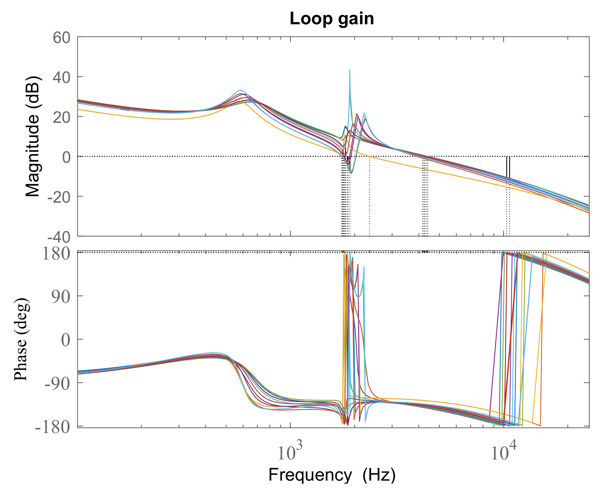
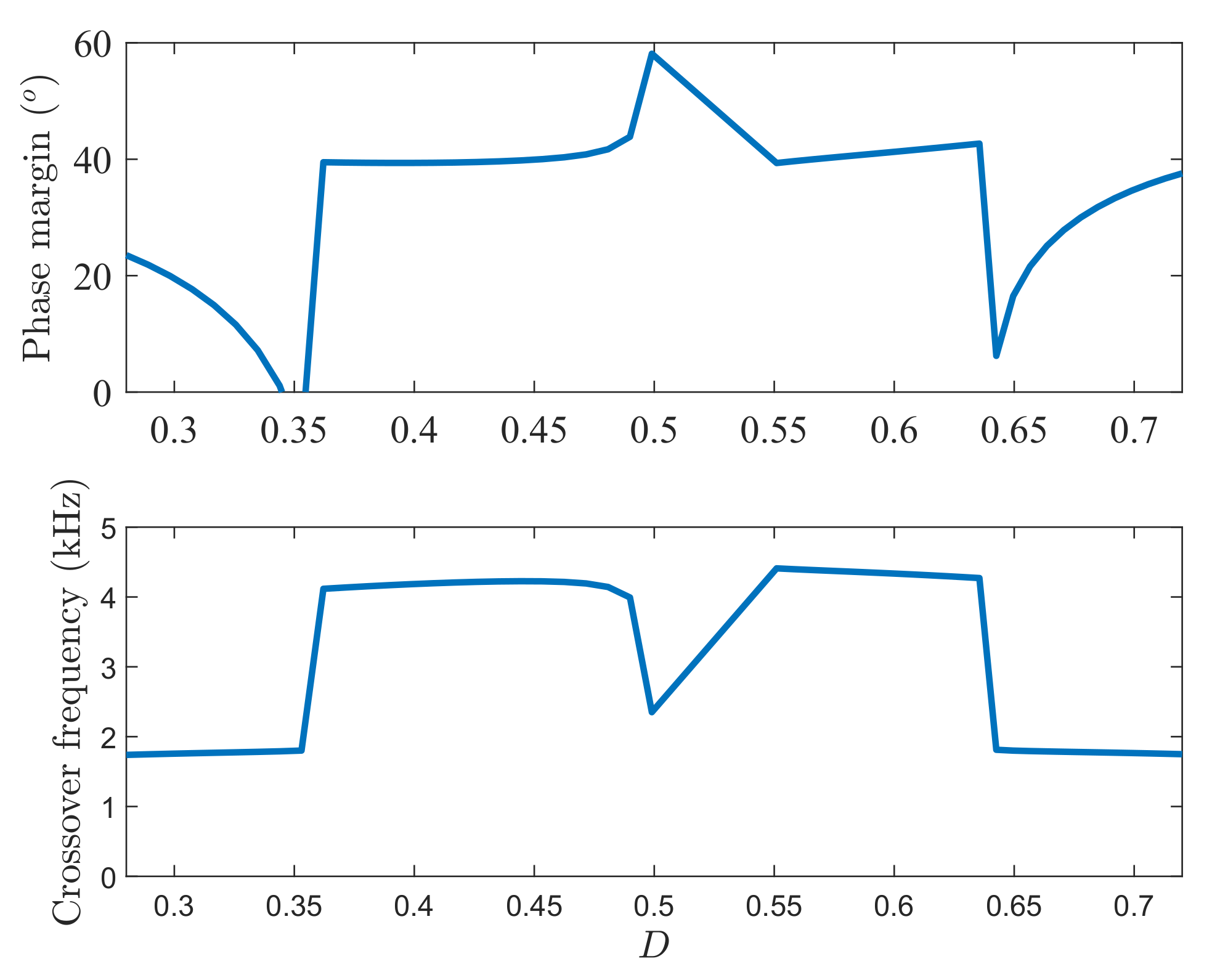
Table 2. First, the different controller design is performed according to the theoretical analysis provided in the previous section. In particular, using the bode plot shown in Figure 9, a crossover frequency f c = 1.8 kHz at D = 0.28 was selected with a corresponding phase margin φ m above 40 ° within the entire range of the operating duty cycle. For achieving these values, the gain, the poles and zeros of the type-III controller are selected at the values depicted in Table 2. The value of the amplitude of the ramp compensator is selected in such a way to avoid subharmonic oscillation within the entire range of the considered duty cycle values.
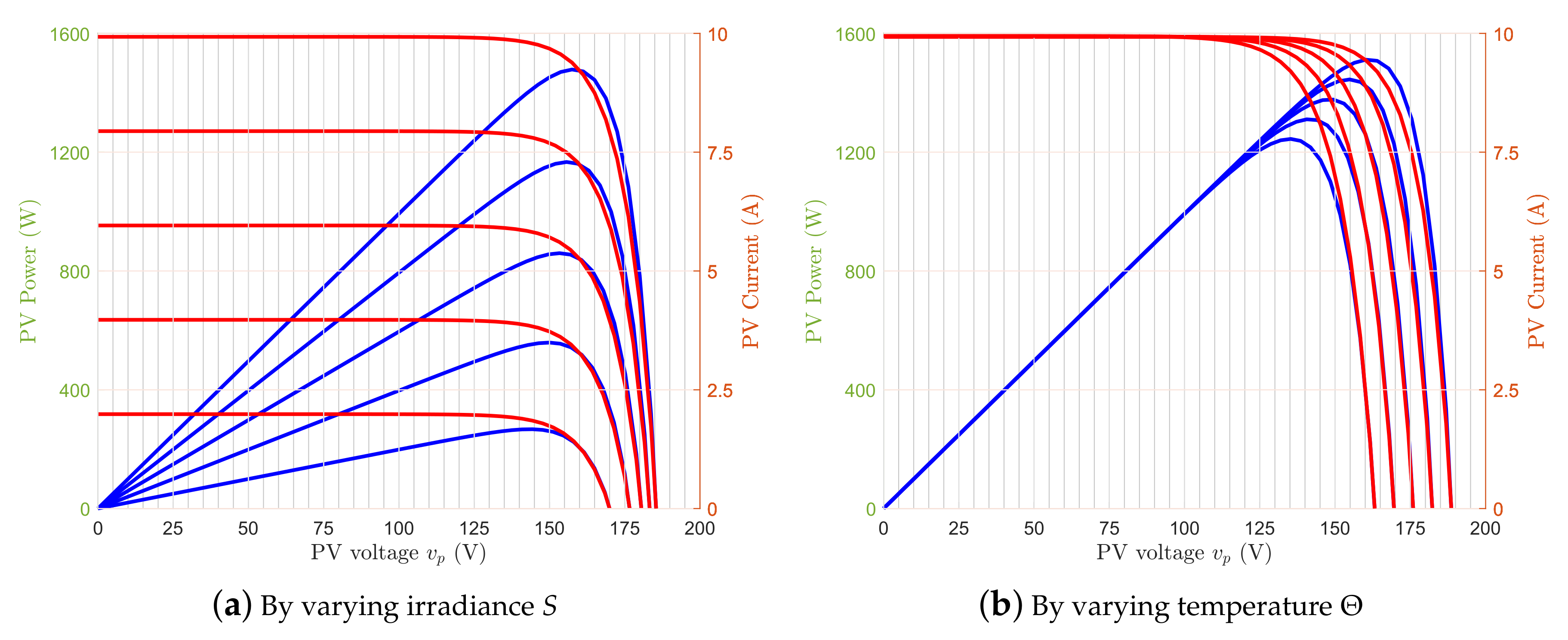
The used PV generator consists of a string of four series-connected modules each one with a maximum power point voltage V mpp = 38.4 V, a maximum power current I mpp = 9.13 A and a maximum power 350 (4 × 350 W = 1.4 kW) at standard test conditions. The manufacturer specifications for one single module are detailed in [32] and summarized in Table 3.
A PV generator from the Renewable Energies library of PSIM © software was used as an input to the inverter. The PV generator block has two inputs one corresponds to irradiance S in W/m 2 and another to temperature Θ in ° C. The temperature was maintained constant and the irradiance profile was defined by a piecewise linear signal generator which is connected to its corresponding PV generator input. The PV source is connected to a 50 Hz grid via the DC–AC differential boost inverter which converts the 154 V DC link PV voltage to 230 V RMS AC with power factor control. The MPPT was implemented in the inverter by means of a C block model using the P&O algorithm which provides the reference for the PV DC voltage. A PI regulator is used to control the PV voltage to its desired reference value. The design of the PV DC-link voltage controller was performed analytically based on the reduced-order model (31). Using this expression, the parameters of this controller have been selected to provide a settling time of one grid voltage cycle. The sampling period of the MPPT controller has been chosen to be equal to five times this settling time. The sampling period is T mppt = 0.1 s and the perturbation amplitude applied to V mpp is Δ V mpp = 4 V.
According to (36), with value of the extracted power and the grid frequency and the value of the DC-link capacitance C dc , the AC-ripple of the PV voltage amplitude is about 7.5 % of its nominal value 154 V at irradiance S = 1000 W/m 2 and temperature Θ = 25 ° C with a maximum power 1.4 kW.
The inverter control system uses three control loops: a first loop which regulates DC link PV voltage to 154 V, a second loop which regulates the grid current to its desired reference which synchronized to the grid voltage. The reference for the grid current is the output of the PV DC voltage external controller. The output of the grid current controller (a type-III controller) is first limited to an upper bound of about I lim = 50 A to avoid inrush current during startup. A ramp compensator is added to the sensed voltage R s L ( i 1 i 2 ) and the result is used as one of the inputs to the comparator. The calculated minimum value needed for avoiding subharmonic oscillation is V M = 3.5 V. Here, to play it safe, a larger value of V M = 5 V is used. The other input is the grid current reference converted to voltage by multiplying it by the current sensor gain R s L . The output of the comparator is connected to the Reset of a flip-flop and a 50 kHz periodic clock signal is connected to its Set input. The driving signal u for the switches Q 2 and Q 4 and 1 u for Q 1 and Q 3 are the outputs Q and Q ¯ of the flip-flop. The inverter control system uses three control loops: a first loop which regulates DC link PV voltage to 154 V, a second loop which regulates the grid current to its desired reference which synchronized to the grid voltage. The reference for the grid current is the output of the PV DC voltage external controller. The output of the grid current controller (a type-III controller) is first limited to an upper bound of about I lim = 50 A to avoid inrush current during startup. A ramp compensator with amplitude V M = 5 V is added to the sensed voltage R s L ( i 1 i 2 ) and the result is used as one of the input to the comparator. The calculated minimum value needed for avoiding subharmonic oscillation is V M = 3.5 V. Here, to pay it safe, a larger value of V M was used. The other input is the grid current reference is converted to voltage by multiplying it by the current sensor gain R s L . The output of the comparator is connected to the Reset pin of a flip-flop and a 50 kHz periodic clock signal is connected to its Set input. The driving signals u for the switches Q 2 and Q 4 and 1 u for Q 1 and Q 3 are the outputs Q and Q ¯ of the flip-flop.
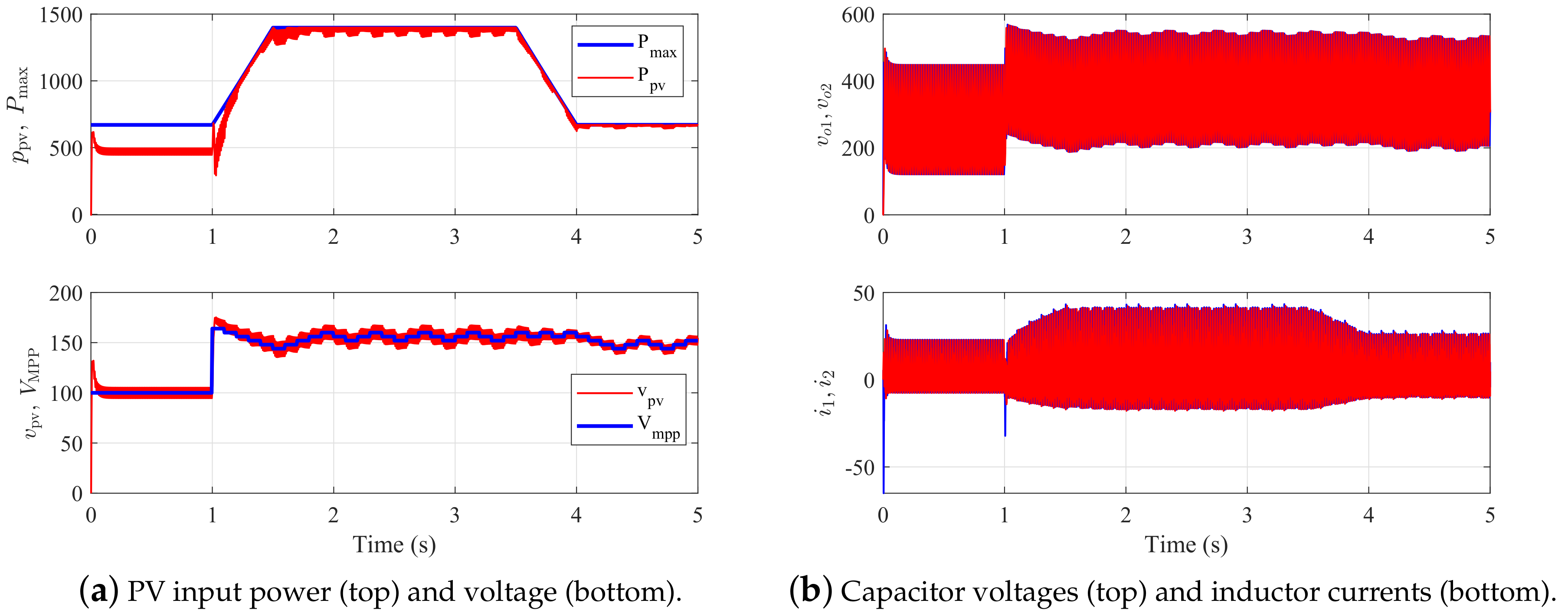
The simulation starts with temperature Θ = 25 ° C and irradiance S = 1000 W/m 2 . The time-domain response of the complete system starting from zero initial conditions is depicted in Figure 10. From t = 0 s to t = 1 s, the inverter is operated with constant reference voltage 100 V and the MPPT control is blocked. The irradiance level is started at S = 500 W/m 2 and the corresponding maximum power is 670 W. It can be observed that during this period, the voltage is well regulated to its reference value 100 V and since MPPT control is not used, the extracted power is less than what the PV generator can deliver.
At t = 1 s, the MPPT is enabled and the irradiance starts increasing. It can be observed that after a short transient, the DC link PV voltage is regulated at V dc = 154 V and the extracted power is very close to the maximum power corresponding to the irradiance level profile. At t = 2 s, the MPPT is still enabled and the irradiance is maintained at 1000 W/m 2 . The PV array output power is about 1.4 kW (see p pv plot on the left panel in Figure 10) whereas specified maximum power with a 1000 W/m 2 irradiance is 1.4 kW. Maximum power (1.4 kW) is obtained when the voltage reference provided by the MPPT controller is 154 V.
At t = 3 s, the irradiance is ramped down from 1000 W/m 2 to 500 W/m 2 and consequently the maximum power decreases. The PV voltage is still regulated and the power extracted by the inverter follows the maximum power delivered by the PV generator during all the time. PV array average voltage is still very close to 154 V in a good agreement with the value expected from PV module specifications. From t = 4.5 s to t = 5 s, sun irradiance is maintained at 500 W/m 2 and MPPT continues to track the maximum power.
On the other hand, under irradiance changes, the DC-link PV voltage V dc , undergoes a very small change and remains very close to the MPP voltage and the PI controller is capable of maintaining the voltage V dc at the desired value after short transient period (0.02 s) due MPPT perturbations. The results clearly demonstrate the capability of the designed system to operate at the MPP regardless of the value of the irradiance and the MPPT control is capable of tracking the MPP when irradiance vary.
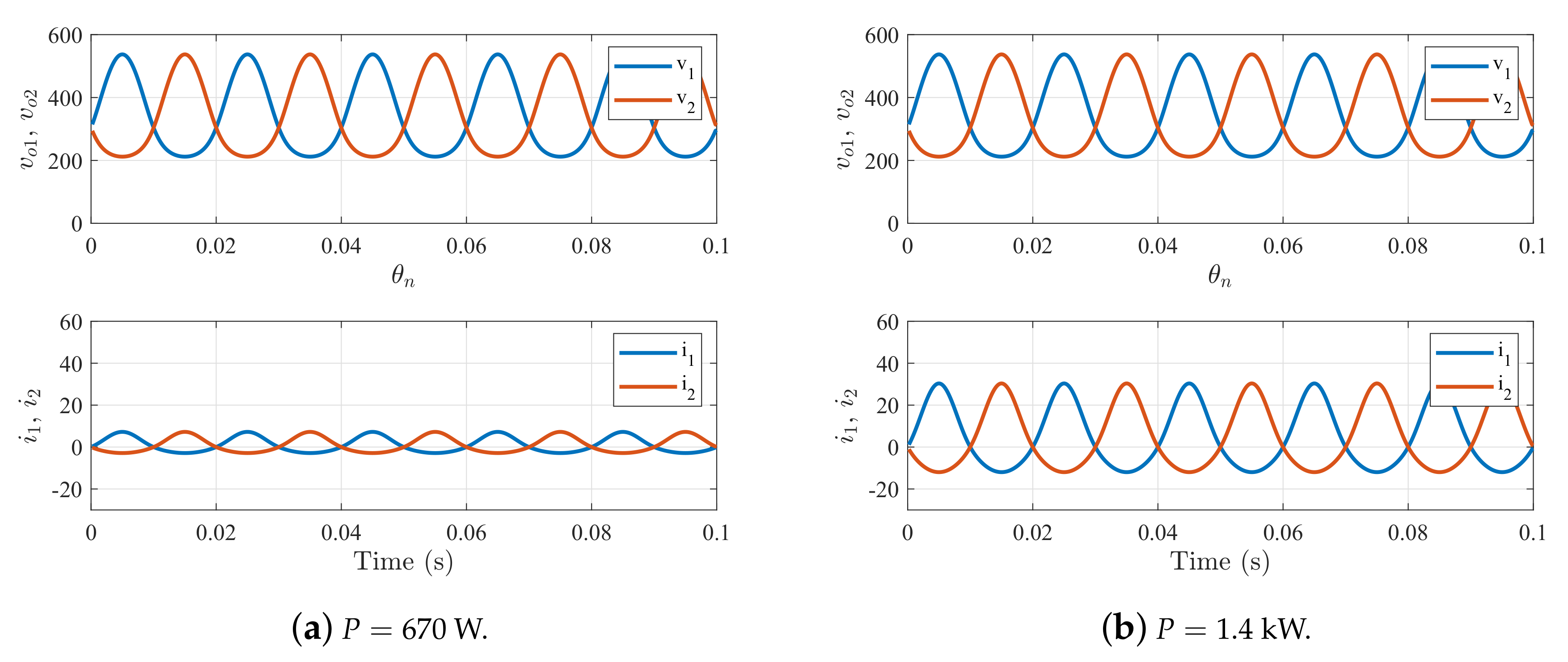
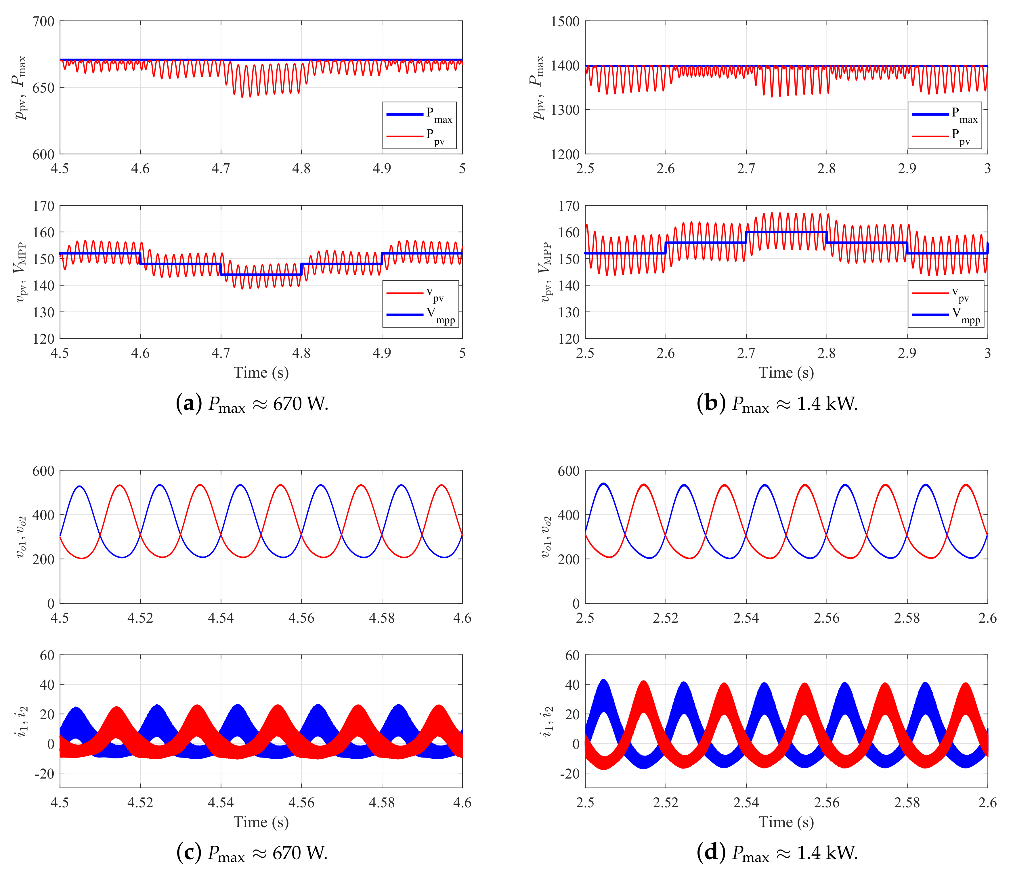
Figure 11 shows the steady-state waveforms of the PV voltage and its reference, the extracted power, the power P from the PV source and its maximum power P max , the inductor currents i 1 and i 2 and the capacitor voltages v o 1 and v o 2 for irradiance level S = 500 W / m 2 ( P max 670 W ) and 1000 W / m 2 ( P max 1.4 kW). It can be observed that in the vicinity of the MPP, the reference voltage V mpp dictated by the MPPT controller oscillates according to the values of the MPPT sampling period T mppt = 0.1 s and the perturbation amplitude Δ V mpp = 4 V as shown in Figure 11a,b for the two different values of the sun irradiance. The inductor currents and capacitor voltage are well balanced and are phase shifted by 180 ° as depicted in Figure 11c,d for the same values of the sun irradiance level. Moreover, the steady-state averaged values of the capacitor voltages and the inductor current are in a close agreement with the theoretical predictions given in (8)–(11) and depicted in Figure 5. Note also that, the DC PV voltage is regulated to the MPP voltage and that it is practically a sinusoidal signal as predicted by (37) with DC component equal to V mpp ± Δ V mpp dictated by the MPPT controller during the MPPT sampling period T mppt = 0.1 s and peak-to-peak AC ripple Δ v ¯ dc 14.65 V for P max = 1.4 kW and it is Δ v ¯ dc 7.02 V for P max = 670 W in a remarkable agreement with (36).
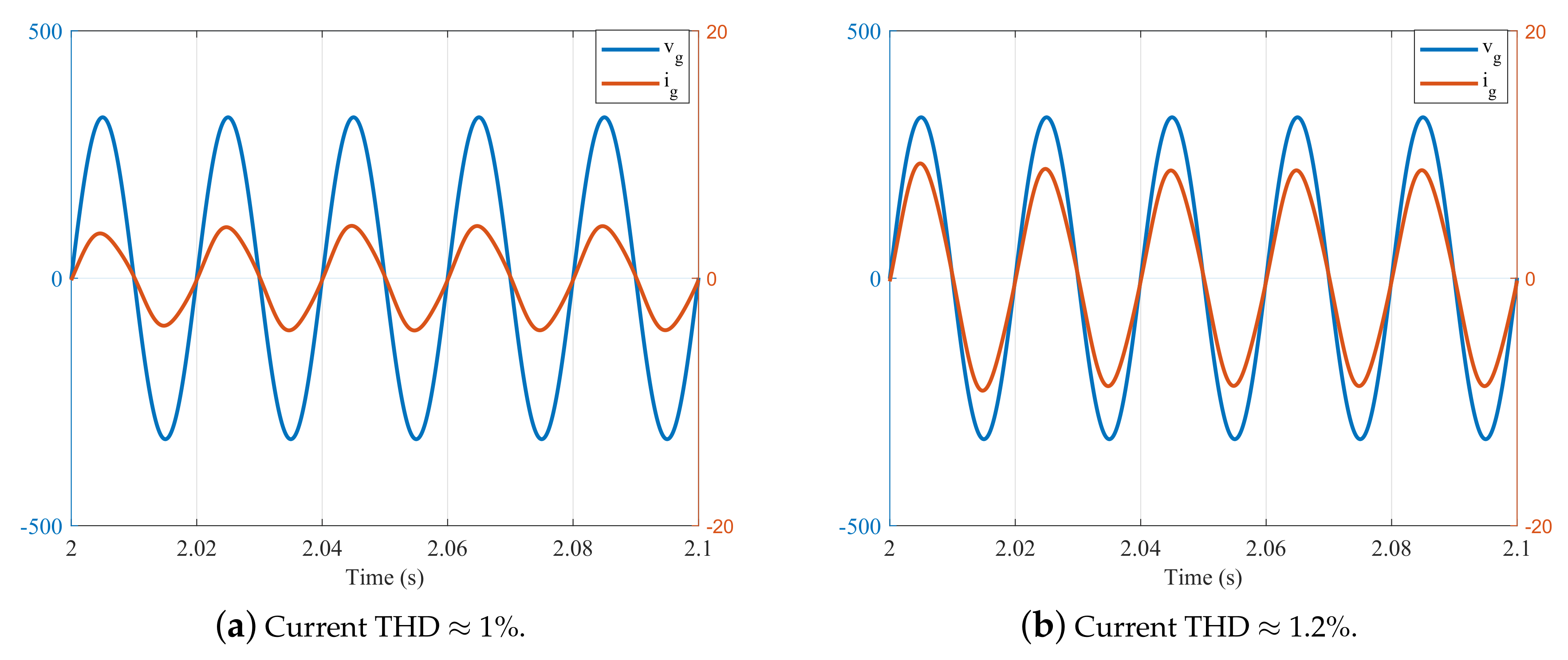
Figure 12 shows the steady-state waveforms of the grid current i g together with the grid voltage v g for irradiance level S = 500 W / m 2 ( P max 670 W) and 1000 W / m 2 ( P max 1.4 kW). Observe that grid voltage and current are in phase and have practically the same sinusoidal shape demonstrating a close to unity power factor. Moreover, the steady-state averaged values of the grid current is in a close agreement with the theoretical predictions. Namely, for irradiance level S = 500 W / m 2 ( P max 670 W), the RMS value of the grid current i g is about 2.91 A and for S = 1000 W / m 2 ( P max 1.4 kW), the RMS value of i g is about 6.1 A. To check the power quality, the THD of the grid current i g in steady-state was calculated for both values of the irradiance. Namely, for irradiance level S = 500 W / m 2 ( P max 670 W), the THD value of the grid current i g is about 1% and for S = 1000 W / m 2 ( P max 1.4 kW), the THD value of i g is about 1.2%. Therefore, it can be observed that the grid current i g exhibits a low THD of about 1 % as calculated by PSIM © software for both values of sun irradiance level. The values are comparable to the ones obtained experimentally in [26] where it was shown that the grid current spectrum comply with the IEEE standard 1547.

6. Conclusions

In contrast to the conventional H-bridge inverter, the differential boost inverter is a flexible DC–AC inverter topology providing voltage step-up capability and could be a potential candidate for many DC–AC electrical energy conversion applications. In this work, the modeling procedures and the multiple control design of a single-stage grid-connected DC–AC differential boost inverter has been addressed. By applying the same reasoning and procedures used for DC–DC converters and based on the frequency response of the inverter in the quasi-steady sense, average models of the inverter under a differential current mode control has been developed. This large-signal model has been used to derive the small-signal model in the frequency domain and based on the obtained frequency response, the controller design has been addressed. Steady-state analysis including the derivation of the AC ripple PV voltage has been performed and a design procedure of the system power stage parameters and controllers has been presented. It has been shown that the differential boost inverter can exhibit interesting features when used in single stage PV systems with the conventional hill climbing MPPT scheme based on P&O algorithm by which the operating voltage of the PV generator can be controlled by perturbing its desired reference and observing the resulting effect on the extracted power. This includes a reduced number of components, low THD and optimal power tracking with standard design procedures for the multiple loop controller. These features have been verified using computer simulations performed on the switched model of the converter under several weather conditions. The entire simulation was performed in the PSIM © software. The results have shown robustness in the grid-connected solar system based on the differential boost inverter. Therefore, the differential boost inverter topology could be suitable for solving challenges in renewable energy such as plug-and-play type AC modules or providing power supply for rural region among others. Future works will deal with the experimental implementation of the inverter with the considered multiple-loop controller when used in a microgrid including storage batteries and other power converters and loads.

Author Contributions

Conceptualization, A.E.A.; Methodology, A.E.A. Software, A.E.A.; Validation, M.A.-N.; Formal Analysis, A.E.A. and M.A.-N.; Investigation, A.E.A.; Resources, M.A.-N.; Data Curation, R.H.; Writing—Original Draft Preparation, A.E.A.; Writing—Review & Editing, M.A.-N. and and M.H.; Visualization, M.A.-N., R.H. and M.H.; Supervision, M.A.-N.; Funding Acquisition, M.A.-N. All authors have read and agreed to the published version of the manuscript.

Funding

This work has been sponsored by the Spanish Agencia Estatal de Investigación (AEI) and the Fondo Europeo de Desarrollo Regional (FEDER) under grants DPI2017-84572-C2-1-R. A. El Aroudi and M. Al-Numay acknowledge financial support from the Researchers Supporting Project number (RSP-2020/150), King Saud University, Riyadh, Saudi Arabia.

Conflicts of Interest

The authors declare no conflict of interest.

Abbreviations

The following abbreviations are used in this manuscript:
CMCCurrent Mode Control
MPPMaximum Power Point
MPPTMaximum Power Point Tracking
PFCPower Factor Correction
PLLPhase Locked Loop
P&OPerturb-and-Observe
PVPhotovoltaic
PWMPulse Width Modulation

References

  1. Richardson, D.B. Electric vehicles and the electric grid: A review of modeling approaches, impacts, and renewable energy integration. Renew. Sustain. Energy Rev. 2013, 19, 247–254. [Google Scholar] [CrossRef]
  2. Alajmi, B.N.; Ahmed, K.H.; Finney, S.J.; Williams, B.W. A maximum power point tracking technique for partially shaded photovoltaic systems in microgrids. IEEE Trans. Ind. Electron. 2013, 60, 1596–1606. [Google Scholar] [CrossRef]
  3. Nasir, M.; Khan, H.A.; Hussain, A.; Mateen, L.; Zaffar, N.A. Solar PV-Based scalable dc microgrid for rural electrification in developing regions. IEEE Trans. Sustain. Energy 2018, 9, 390–399. [Google Scholar] [CrossRef]
  4. Kouro, S.; Leon, J.I.; Vinnikov, D.; Franquelo, L.G. Grid-connected Photovoltaic Systems: An Overview of Recent Research and Emerging PV converter technology. IEEE Ind. Electron. Mag. 2015, 9, 47–61. [Google Scholar] [CrossRef]
  5. Meinhardt, M.; Cramer, G. Multi-string converter: The next step in evolution of string converter technology. In Proceedings of the 9th European Power Electronics and Applications Conference (EPE 2001), Graz, Austria, 27–29 August 2001; pp. 27–28. [Google Scholar]
  6. Carbone, R.; Tomaselli, A. Recent advances on AC PV-modules for grid-connected photovoltaic plants. In Proceedings of the 2011 International Conference on Clean Electrical Power (ICCEP), Ischia, Italy, 14–16 June 2011; pp. 124–129. [Google Scholar]
  7. Fang, Y.; Zhu, Y.; Fei, J. Adaptive Intelligent Sliding Mode Control of a Photovoltaic Grid-Connected Inverter. Appl. Sci. 2018, 8, 1756. [Google Scholar] [CrossRef] [Green Version]
  8. Jain, S.; Agarwal, V. A Single-stage grid connected inverter topology for solar PV systems with maximum power point tracking. IEEE Trans. Power Electron. 2007, 22, 1928–1940. [Google Scholar] [CrossRef] [Green Version]
  9. Liao, Z.-X.; Luo, D.; Luo, X.-S.; Li, H.-S.; Xiang, Q.-Q.; Huang, G.-X.; Li, T.-H.; Jiang, P.-Q. Nonlinear Model and Dynamic Behavior of Photovoltaic Grid-Connected Inverter. Appl. Sci. 2020, 10, 2120. [Google Scholar] [CrossRef] [Green Version]
  10. Pavan, A.M.; Castellan, S.; Quaia, S.; Roitti, S.; Sulligoi, G. Power electronic conditioning systems for industrial photovoltaic fields: Centralized or string inverters? In Proceedings of the 2007 International Conference on Clean Electrical Power, Capri, Italy, 21–23 May 2007; pp. 208–214. [Google Scholar]
  11. Sivasubramanian, P.T.; Mazumder, S.K.; Soni, H.; Gupta, A.; Kumar, N. A DC–DC modular current-source differential-mode inverter. IEEE J. Emerg. Sel. Top. Power Electron. 2016, 4, 489–503. [Google Scholar] [CrossRef]
  12. Peng, F.Z. Z-source inverter. IEEE Trans. Ind. Appl. 2003, 39, 504–510. [Google Scholar] [CrossRef]
  13. Anderson, Y.; Li, J.; Peng, F.Z.; Liu, D. Quasi Z-source inverter for photovoltaic power generation systems. In Proceedings of the 2009 Twenty-Fourth Annual IEEE Applied Power Electronics Conference and Exposition, Washington, DC, USA, 15–19 February 2009; pp. 918–924. [Google Scholar]
  14. Ge, B.; Abu-Rub, H.; Peng, F.Z.; Lei, Q.; de Almeida, A.T.; Ferreira, F.J.T.E.; Sun, D.; Liu, Y. An energy-stored quasi-Z-source inverter for application to photovoltaic power system. IEEE Trans. Ind. Electron. 2013, 60, 4468–4481. [Google Scholar] [CrossRef]
  15. Caceres, R.O.; Barbi, I. A boost DC—AC converter: Analysis, design, and experimentation. IEEE Trans. Power Electron. 1999, 14, 134–141. [Google Scholar] [CrossRef]
  16. Vazquez, N.; Almazan, J.; Alvarez, J.; Aguilar, C.; Arau, J. Analysis and experimental study of the buck, boost and buck-boost inverters. In Proceedings of the 30th Annual IEEE Power Electronics Specialists Conference. Record. (Cat. No.99CH36321), Charleston, SC, USA, 1 July 1999; Volume 2, pp. 801–806. [Google Scholar]
  17. Jang, M.; Agelidis, V.G. A Minimum Power-Processing-Stage Fuel-Cell Energy System Based on a Boost-Inverter with a Bidirectional Backup Battery Storage. IEEE Trans. Power Electron. 2011, 26, 1568–1577. [Google Scholar] [CrossRef]
  18. Zhu, G.; Tan, S.; Chen, Y.; Tse, C.K. Mitigation of Low-Frequency Current Ripple in Fuel-Cell Inverter Systems through Waveform Control. IEEE Trans. Power Electron. 2013, 28, 779–792. [Google Scholar] [CrossRef] [Green Version]
  19. Jha, K.; Mishra, S.; Joshi, A. High-Quality Sine Wave Generation Using a Differential Boost Inverter at Higher Operating Frequency. IEEE Trans. Ind. Appl. 2015, 51, 373–384. [Google Scholar] [CrossRef]
  20. Sanchis, P.; Ursaea, A.; Gubia, E.; Marroyo, L. Boost DC–AC inverter: A new control strategy. IEEE Trans. Power Electron. 2005, 20, 343–353. [Google Scholar] [CrossRef]
  21. Flores-Bahamonde, F.; Valderrama-Blavi, H.; Bosque-Moncusi, J.M.; García, G.; Martínez-Salamero, L. Using the sliding-mode control approach for analysis and design of the boost inverter. IET Power Electron. 2016, 9, 1625–1634. [Google Scholar] [CrossRef]
  22. Albea, C.; Gordillo, F.; Canudas de Wit, C. Adaptative control design for a boost inverter. Control Eng. Pract. 2011, 19, 32–44. [Google Scholar] [CrossRef] [Green Version]
  23. Jang, M.; Ciobotaru, M.; Agelidis, V.G. A single-phase grid connected Fuel cell system based on a boost-inverter. IEEE Trans. Power Electron. 2013, 28, 279–288. [Google Scholar] [CrossRef]
  24. Abeywardana, D.B.W.; Hredzak, B.; Agelidis, V.G. A Rule-Based Controller to Mitigate DC-Side Second-Order Harmonic Current in a Single-Phase Boost Inverter. IEEE Trans. Power Electron. 2016, 31, 1665–1679. [Google Scholar] [CrossRef]
  25. Wei, Z.; Lu, D.D.-C.; Agelidis, V.G. Current control of grid-connected boost inverter with zero steady-state error. IEEE Trans. Power Electron. 2011, 26, 2825–2834. [Google Scholar]
  26. Lopez-Caiza, D.; Flores-Bahamonde, F.; Kouro, S.; Santana, V.; Müller, N.; Chub, A. Sliding mode based control of dual boost inverter for grid connection. Energies 2019, 12, 4241. [Google Scholar] [CrossRef] [Green Version]
  27. Lopez, D.; Flores-Bahamonde, F.; Kouro, S.; Perez, M.A.; Llor, A.; Martínez-Salamero, L. Predictive control of a single-stage boost DC–AC photovoltaic microinverter. In Proceedings of the IECON 2016 42nd Annual Conference of the IEEE Industrial Electronics Society, Florence, Italy, 23–26 October 2016; pp. 6746–6751. [Google Scholar]
  28. Cortes, D.; Vazquez, N.; Alvarez-Gallegos, J. Dynamical sliding-mode control of the boost inverter. IEEE Trans. Ind. Electron. 2009, 56, 3467–3476. [Google Scholar] [CrossRef]
  29. Kuperman, A. Proportional resonant current controllers design based on desired transient performance. IEEE Trans. Power Electron. 2015, 23, 5341–5345. [Google Scholar] [CrossRef]
  30. Mattingly, D. Designing Stable Compensation Networks for Single Phase Voltage Mode Buck Regulators; Technical Brief; Intersil: Milpitas, CA, USA, 2003. [Google Scholar]
  31. El Aroudi, A.; Al-Numay, M.; Garcia, G.; Al Hossani, K.; Al Sayari, N.; Cid-Pastor, A. Analysis of nonlinear dynamics of a quadratic boost converter used for maximum power point tracking in a grid-interlinked PV system. Energies 2019, 12, 61. [Google Scholar] [CrossRef] [Green Version]
  32. Available online: http://static.trinasolar.com/sites/default/files/US-Datasheet-DD14A(II).pdf (accessed on 25 April 2019).
  33. Available online: https://powersimtech.com/products/psim/ (accessed on 7 July 2020).
Figure 1. The concept of building a differential inverter using two DC–DC converters.
Applsci 10 04808 g001
Figure 2. Single-stage grid-connected PV-fed differential boost inverter.
Applsci 10 04808 g002
Figure 3. Block diagram of the control system for the single-stage grid-connected PV-fed boost inverter.
Applsci 10 04808 g003
Figure 4. PV curves for different values of irradiance S in the range (200,1000) W/m 2 and temperature Θ = 25 ° C and for different values of temperature in the range (20,60) ° C and for irradiance S = 1000 W/m 2 .
Applsci 10 04808 g004
Figure 5. Steady-state waveforms of the average inductor currents and capacitor voltages of the differential boost inverter from the quasi-steady-state analytical expressions (8)–(11) for two different values of power P = 670 W and P = 1.4 kW by assuming a unity power factor.
Applsci 10 04808 g005
Figure 6. Pole-zero plot of the differential boost inverter showing likely pole-zero pair cancellation when duty cycle D varies in the range (0.28, 0.72) for S = 1000 W / m 2 and Θ = 25 ° C. The zero at high frequency is invariant under the duty cycle variation. (a) Overall view when D is varied, (b) Close view in the vicinity of the imaginary axis.
Applsci 10 04808 g006
Figure 7. Frequency response of the differential boost inverter when duty cycle varies in the range (0.28, 0.72) for S = 1000 W / m 2 and Θ = 25 ° C.
Applsci 10 04808 g007
Figure 8. Loop gain frequency response for the differential boost inverter for S = 1000 W / m 2 ( P max 1.4 kW) and Θ = 25 ° C when the duty cycle is varied in the range ( 0.28 , 0.72 ) .
Applsci 10 04808 g008
Figure 9. Phase margin and crossover frequency of the loop gain frequency response for the differential boost inverter for S = 1000 W / m 2 ( P max 1.4 kW) and Θ = 25 ° C when the duty cycle is varied in the range ( 0.28 , 0.72 ) .
Applsci 10 04808 g009
Figure 10. Startup and steady-state behavior and response to changes in the irradiance level of the boost inverter between 500 W / m 2 ( P max 670 W ) and 1000 W / m 2 ( P max 1.4 kW). Θ = 25 ° C.
Applsci 10 04808 g010
Figure 11. Steady-state response of boost inverter with the multiple-loop control for two different values of the irradiance S between 500 W / m 2 ( P max 670 W) and 1000 W / m 2 ( P max 1.4 kW). Θ = 25 ° C.
Applsci 10 04808 g011
Figure 12. Steady-state waveforms of the grid voltage and the grid current delivered by the differential boost inverter for S = 500 W / m 2 ( P max 670 W) and S = 1000 W / m 2 ( P max 1.4 kW). Θ = 25 ° C.
Applsci 10 04808 g012
Table 1. The used parameters for the DC–AC differential boost inverter power stage.
ParameterValue
Inductance L 1 = L 2 = L and L g 100 μ H and 5 mH
Capacitance C 1 = C 2 = C 22 μ F
PV DC-link capacitance C dc 2 mF
PWM switching frequency f s 50 kHz
Table 2. The used parameters for the different loop controllers of the DC–AC differential boost inverter.
ParameterValue
Current sensors gains R s L and R s g 0.1 Ω and 1 Ω
Time constant τ of the PV voltage PI controller0.0247 s
Proportional gain K p , v of the PV voltage PI controller0.2
Cut-off frequency of the PV voltage filter ω c / ( 2 π ) 50 Hz
Zeros ω z / ( 2 π ) and poles ω p / ( 2 π ) of the type-III controller ω z / ( 2 π ) 500 Hz and 50 kHz
Proportional gain K p , c of the grid current type-III controller2
Table 3. The parameters of one single module forming the used PV panel.
ParameterValue
Number of series-connected cells in a module 72
Open-circuit voltage of a module V o c 46.5 V
Short-circuit current I s c 9.60 A
PV voltage at maximum power V mpp 38.4 V
PV current at maximum power I mpp 9.13 A

