1. Introduction
The solar industry has been attracting attention as a future energy source, and the demand and supply market for crystalline silicon (c-Si) solar cells has been gradually expanding. However, the maximum efficiency of conventional c-Si solar cell fabrication technology is limited, so it is necessary to study this technology in order to improve its efficiency [
1,
2,
3]. Currently, new methods of increasing efficiency involve cell design modifications using selective emitters [
4]. In contrast to a conventional single emitter, a selective emitter is a heavily doped region with a large depth of impurity diffusion in the electrode region. In addition, a lightly doped region with a small depth of impurity diffusion is formed in the non-electrode region. A heavily doped region can reduce the contact resistance between the front electrode and the emitter, and it can increase the open-circuit voltage (V
oc). However, the recombination velocity increases and the carrier lifetime decreases due to the scattering effect with excessive impurities. In contrast, a lightly doped region reduces the recombination at the surface and offers excellent quantum efficiency characteristics in the short wavelength region. Selective emitter solar cells can increase efficiency by utilizing low-concentration and high-concentration emitters. Among the methods of forming a selective emitter structure, the laser process can be an advantageous alternative for creating doped contacts in solar cells because of its simple fabrication process that avoids the high temperature and photolithography steps in the opening and simultaneously dopes of the base and emitter contacts. An emitter formation process is carried out in a laser doping selective emitter (LDSE) solar cell to diffuse phosphorus (P) into the wafer to form a p–n junction. Next, the laser process step is carried out in the formation area of the selective emitter [
5]. The electrode surface is processed using a laser with respect to the area where the electrode should be located.
A laser-assisted LDSE is capable of offering high output and a high repetition rate; hence, it is possible to achieve high throughput and production. In addition, lasers can create LDSE structures using a one-step process, which is unlike conventional techniques that require multiple steps such as mask deposition, chemical etching, and high-temperature diffusion [
6,
7]. This laser process leads to the diffusion of additional P atoms from the phosphorus silicate glass (PSG) layer, which is generated during the doping process, and high doping for already-diffused P atoms. The resistance of the sheet area where the laser process is carried out is less than that of the sheet area where the laser process is not carried out. The University of New South Wales (UNSW) School of Photovoltaics and Renewable Energy Engineering developed a technology for the laser doping of a selective emitter solar cell. As a result of the present research, the contact resistivity between the electrode and silicon wafer generated using the conventional screen printing method was significantly reduced by applying a laser doping selective emitter [
8,
9]. This paper is divided into the following sections. First, we studied a weak emitter formed from a POCl
3 (phosphorus oxychloride) tube furnace and determined the different doping profiles. Next, the effect of the laser doping step on the selective emitters was analyzed using the optimized laser parameters. The selective emitter structures were irradiated using a range of laser processing conditions to determine the effects of the laser frequency, wavelength, laser fluence, and laser speed on the dopant profile and diode characteristics. Additionally, the same processes for different laser conditions were performed to achieve a high doping efficiency at a relatively low laser fluence, resulting in reduced laser-induced damages.
3. Results and Discussion
To optimize the pre-diffusion process and to form a uniform emitter layer, the pre-diffusion process was performed for 12 min, and the process temperature was increased from 780 to 830 °C in 10 °C intervals. The drive-in process was performed for 14 min, and the process temperature was increased from 810 to 890 °C in 20 °C intervals.
Figure 1 shows the graph of the surface resistance in the emitter layer with a temperature difference between the pre-deposition and diffusion processes. The surface resistances were measured at five points of the wafer where the emitter layer was formed, and the change in the sheet resistance depending on the pre-deposition and drive-in temperatures showed a similar trend. The sheet resistance decreased with the increasing temperatures of the deposition and drive-in processes because the higher the pre-deposition temperature, the greater the influence of diffusion of dopants deposited on the wafer surface. At a drive-in temperature of 810 °C, the measured resistance value was high and unsuitable for the diode of a solar cell. The diffusion equation can be expressed as
, where
is the flux (g/cm
2·sec),
N is the impurity concentration, and
D is the diffusion coefficient.
D is the proportionality constant that was applied because the dependence of temperature on thermal motion varies depending on the particle type. The formula for
D can be expressed as
, where
EA is the activation energy (J/mol),
D0 is the pre-exponential factor,
k is the Boltzmann constant, and
T is the temperature (
K). An increase in the absolute temperature
T implies an increase in
D [
10,
11]. In other words, an increase in the pre-deposition and drive-in temperature implies an increase in the diffusion flow density and a potential decrease in the sheet resistance.
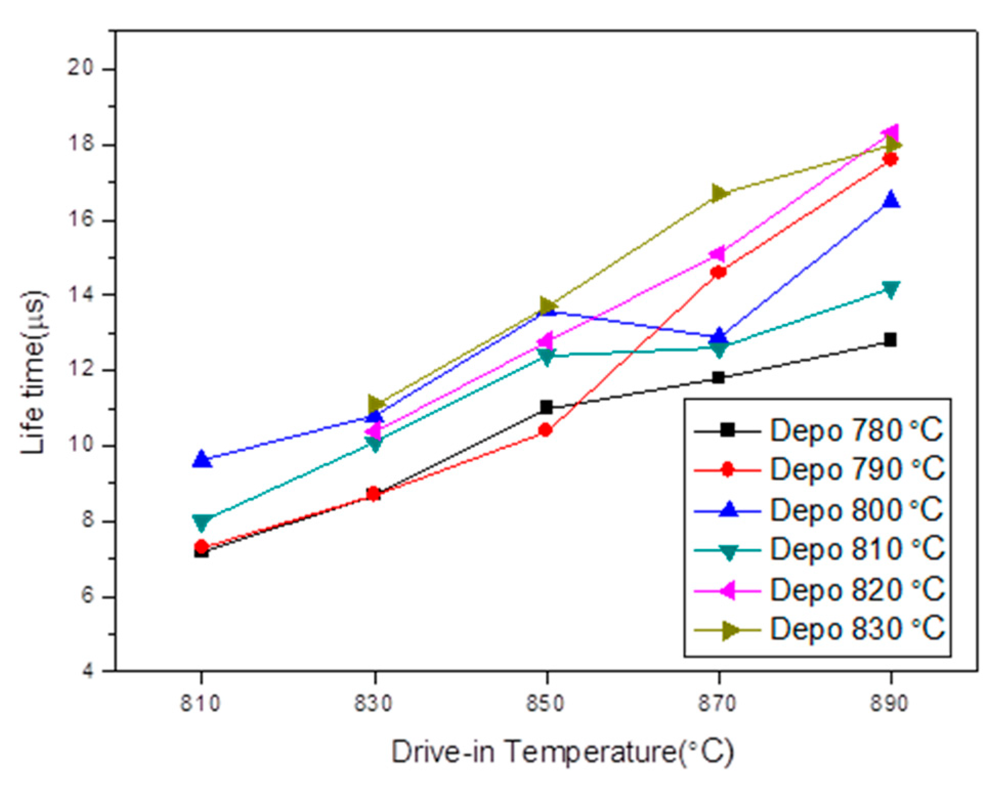
Figure 2 shows a graph of the carrier lifetime measured using the QSSPC by varying the temperature of the pre-deposition and drive-in processes. The carrier lifetime is a major factor in the fabrication of solar cells because it increases the capability of electron collection, which can be directly related to efficiency. As shown in
Figure 2, the carrier lifetime was higher with increasing process temperature because a higher number of carriers could be generated at high process temperatures when the sheet resistance was low due to the high doping concentration of P on the surface and deep inside junction. In addition, when the conditions of the pre-deposition temperature were compared, a higher carrier lifetime (which was an important aspect of solar cell fabrication) of approximately 18 µs at a minority carrier density of
cm
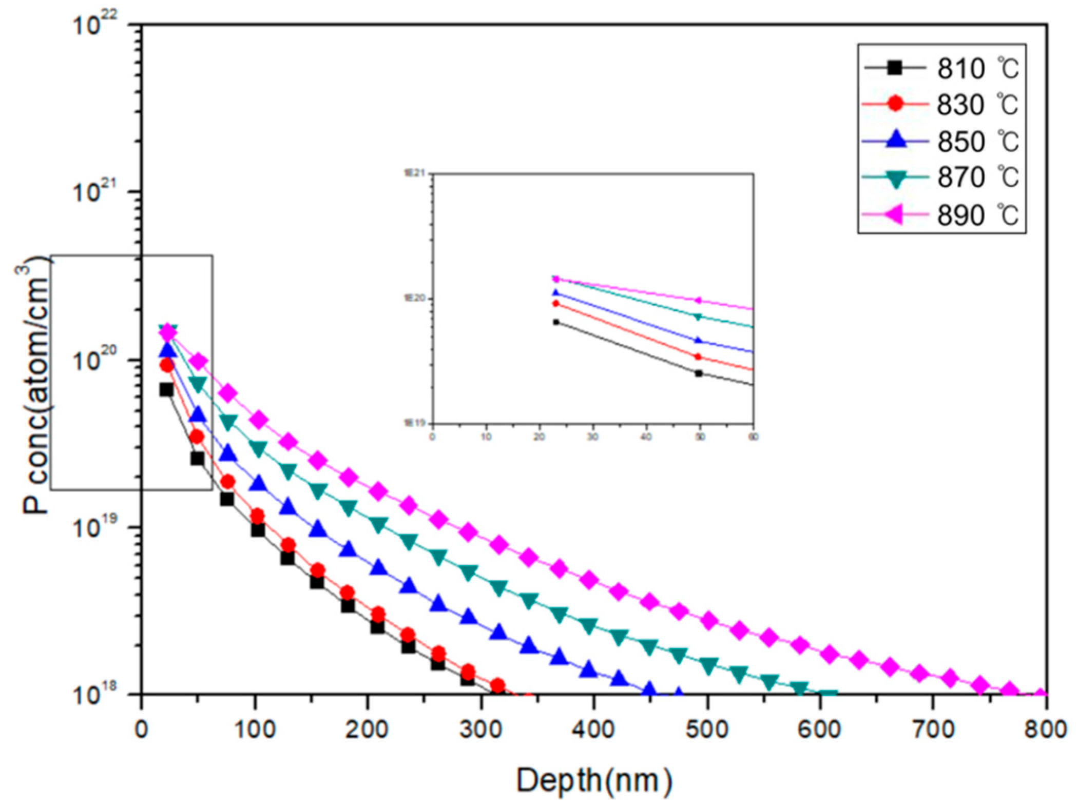
−3 was measured at a low pre-deposition temperature. For the doping process, the drive-in is a process of changing the distribution form of the doping concentration deposited in the pre-deposition step. The concentration at the surface varied with the process temperature. The surface doping concentration and depth of the emitter layer were compared using an SIMS (Secondary-ion mass spectrometry) analysis to measure the profile of the formed emitter layer based on the temperature difference between the pre-deposition and drive-in processes.
Figure 3 shows the SIMS profile of the emitter layer with a difference between the pre-deposition and diffusion processes. After fixing the pre-deposition temperature at 800 °C, the SIMS profile based on the drive-in process temperature was obtained. As the diffusion coefficient and drive-in process temperatures increased, the surface doping concentration and doping depth increased. In the case of the deposition temperature, the surface doping concentration was similar to that of the temperature increase, but the doping depth increased. In the case of the drive-in temperature, the surface doping concentration increased based on the temperature increase, and it also tended to increase proportionally. To confirm the uniformity of surface resistance after the formation of the emitter layer based on the temperature difference between the pre-deposition and drive-in processes, the average value of the sheet resistance was measured at five points of the sample after doping. In the emitter formation process, the doping uniformity was important during the electrode formation and firing. The uniformity of doping represents the uniformity of the concentration distribution and junction depth, which has a considerable effect on the generation of leakage current after the electrode formation and firing processes. As a result, we obtained a lightly doped emitter sample with an average sheet resistance and uniformity of 80.78 Ω/sq and 4.11%, respectively.
The effects of the laser fluence and scan speed (critical laser parameters) were investigated to achieve the optimal conditions for an ideal selective emitter: a sufficiently and heavily doped region and a reduction in the recombination velocity. The resulting doping level, surface melting profile, and damage to the substrate from each laser parameter were discussed. In this study, a heavily doped emitter was formed by a laser using PSG formed in a lightly doped emitter through a POCl
3 diffusion furnace. The spin on doping (SOD) dopant sources were used for the LDSE process, but SOD was not used in this study. Because no additional dopant was administered to silicon (Si), the laser process redistributed the dopant from the thermally diffused phosphor emitter and potentially activated the dopant from the dead layer. Sheet resistance can be significantly reduced without applying SOD. The laser intensity during the LDSE process is an important factor that can determine cell characteristics. In the heavily doped region, the sheet resistance decreased with increasing laser intensity because more dopants entered the emitter layer, and the c-Si wafer could have been destroyed if the laser intensity was excessive. Moreover, because the recombination of the carriers increased due to the surface damage, it was important to find a laser optimization condition that would minimize the laser damage and obtain a high doping concentration. The first laser parameter that was investigated was the laser fluence. The following laser parameters were used in this experiment: a 500 kHz repetition rate and a 100 mm/s laser speed. The laser power was varied from 0.8 to 5.6 W to form a heavily doped emitter. The energy density or fluence was measured in J/cm
2. Therefore, the fluence is mathematically defined as the integral of the power of a single beam pulse over time divided by the spot size of the beam. Because the power meter measures the average beam power over an extended period of time, as expressed by the heat generated by the laser energy, the expression for calculating the fluence can be simplified as
, where
P is the beam power measured by a laser power meter (Watts),
f is the repetition rate or pulsing frequency (Hz), and
D is the beam diameter (cm) [
12]. The laser fluencies corresponding to the laser power of 0.8–5.6 W were 0.3–2.25 J/cm
2, respectively.
Figure 4 shows the graph of the sheet resistance and the amount of decrease in the sheet resistance of the emitter layer with laser fluence after the formation of the LDSE. The results showed that as the laser fluence increased, the doping level increased and sheet resistance decreased. A heavily doped emitter with a sheet resistance of approximately 11–48 Ω/sq was obtained. Under a laser fluence of 0.3 J/cm
2, the laser process failed. The laser energy was used to melt Si, and the diffusion of the dopant atoms occurred in the liquid phase [
13]. However, the energy was insufficient to allow for diffusion under a laser fluence of 0.3 J/cm
2 or less. At a laser fluence of 0.8 J/cm
2, the sheet resistance was reduced by 32.92 Ω/sq. In addition, it was found that a heavily doped region with a sheet resistance of 11.38 Ω/sq was formed under a laser fluence of 2.25 J/cm
2 because more dopants entered the emitter layer and sheet resistance decreased. In the case of laser doping, damage to the surface of a crystalline wafer is inevitable. Here, the damage caused by laser irradiation on the sample surface was evidenced by cracks, debris, and a melted surface; dislocations and cracks were also observed at the bottom of the sample. In this study, the surface damage caused by laser irradiation was analyzed with SEM.
Figure 5 shows a cross-sectional image of the c-Si wafer with respect to laser fluence. The relationship between surface characteristics and laser fluence after laser doping was analyzed. The results confirmed that when the laser fluence was excessive, the c-Si wafer was destroyed, and the surface characteristics deteriorated due to melting. In addition, a heavily doped region was obtained without breaking the shape of the Si surface pyramid at laser fluencies of 0.8 and 1.29 J/cm
2, so the laser fluence was fixed at those values while the laser speed was varied from 10 to 70 mm/s in order to make an accurate comparison between the two fluence conditions.
The next important parameter was laser speed, which was determined based on the X–Y stage motion speed. Reducing the laser speed increases the percentage of overlap among laser pulses, which can be expressed as
, where
V is the laser scan speed, which was 10, 40, and 70 mm/s;
f (Hz) is the pulse frequency; and
D (mm) is the laser spot size [
14]. A green laser beam with a spot size and frequency of approximately 0.025 mm and 500 kHz, respectively, was used at various laser speeds ranging from 10 (99.92% overlap) to 70 mm/s (99.44% overlap). As the process progressed, a circular wave-shaped process area, called ripple, was formed from the overlapping wave pulses. As the laser speed decreased, a higher degree of overlap occurred during the laser pulse, causing the ripples to decrease in size and smoothen. In addition, increasing the overlap among the pulses increased the laser time on the wafer, which meant that the doped region had a large amount of cumulative energy from the laser.
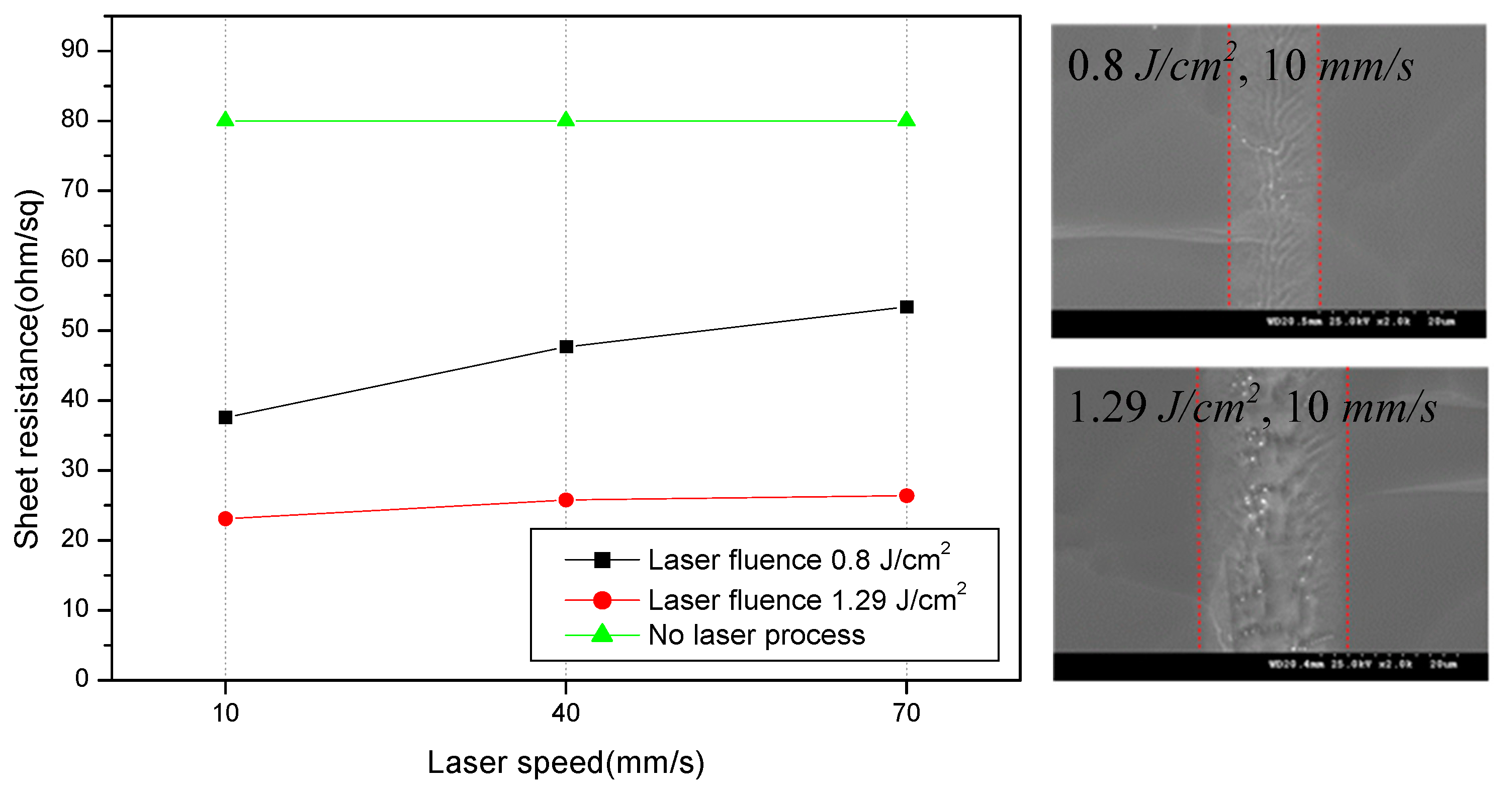
Figure 6 shows the graph of the sheet resistances and their decreasing magnitudes with respect to laser speed after fixing the laser fluence at 0.8 and 1.29 J/cm
2. The change in sheet resistance as a function of laser speed was obtained under a laser fluence of 0.8 J/cm
2; however, this change was small under the laser fluence of 1.29 J/cm
2, which indicated that the dopant diffused into Si could possibly increase with decreasing laser speed under a laser fluence of 0.8 J/cm
2. As shown in the SEM image in
Figure 6, under a laser speed of 10 mm/s, for the two laser fluence conditions, the surface structure deteriorated because of the surface melting caused by the application of the laser for an excessive period in the wafer. The sheet resistances were 43.7 and 59.1 Ω/sq under laser fluencies of 0.8 and 1.29 J/cm
2, respectively. When the laser speed changed under the laser fluence of 0.8 J/cm
2, there was a change in resistance. However, under a laser fluence of 1.29 J/cm
2, there was no change in resistance; therefore, the contact resistance was measured by forming the electrodes for each condition.
Figure 7 shows the contact resistivity with respect to laser fluence and surface image of the Si wafer at different laser fluencies. During this period, the contact resistivity was measured using the TLM, and the laser speed was fixed at 40 mm/s. Contact resistance values of 1.2 and 0.8 mΩ·cm
2 were obtained in the samples under the laser fluencies of 1.77 and 2.25 J/cm
2, respectively; a degradation of characteristics due to laser damage was expected. Based on the SEM image, the heat-affected zone (HAZ) resulting from the deterioration of surface properties due to melting was observed, which was determined to affect the increase in resistance during electrode formation. Under the laser fluence of 0.3 J/cm
2, the density of energy applied to the processing part was low, indicating a high contact resistivity exceeding 56 mΩ·cm
2. As shown in the SEM image, it was found that the laser process did not occur under the laser fluence of 0.3 J/cm
2; hence, the contact resistance value was considered to be that of the conventional solar cell. Based on this, the efficiency of the solar cell was expected to decrease because of the increase in the contact resistance between the electrode and the wafer. Therefore, the process conditions were optimized, demonstrating a low contact resistivity of 3.4 mΩ·cm
2 with minimal surface structural deformation under the laser fluencies of 1.29 and 40 mm/s. This had a lower contact resistance than that of the TLM output of the typical standard cell; hence, a higher efficiency of solar cell was be expected due to the low resistance.


