Article

Low-Noise Multimodal Reconfigurable Sensor Readout Circuit for Voltage/Current/Resistive/Capacitive Microsensors

1
Department of Electronics Engineering, Chungnam National University, Daejeon 34134, Korea
2
National Nanofab Center, Daejeon 34141, Korea
*
Author to whom correspondence should be addressed.
Appl. Sci. 2020, 10(1), 348; https://doi.org/10.3390/app10010348
Submission received: 2 December 2019 / Revised: 27 December 2019 / Accepted: 30 December 2019 / Published: 2 January 2020
(This article belongs to the Special Issue Selected Papers from IMETI 2018)

Abstract

:
This paper presents a low-noise reconfigurable sensor readout circuit with a multimodal sensing chain for voltage/current/resistive/capacitive microsensors such that it can interface with a voltage, current, resistive, or capacitive microsensor, and can be reconfigured for a specific sensor application. The multimodal sensor readout circuit consists of a reconfigurable amplifier, programmable gain amplifier (PGA), low-pass filter (LPF), and analog-to-digital converter (ADC). A chopper stabilization technique was implemented in a multi-path operational amplifier to mitigate 1/f noise and offsets. The 1/f noise and offsets were up-converted by a chopper circuit and caused an output ripple. An AC-coupled ripple rejection loop (RRL) was implemented to reduce the output ripple caused by the chopper. When the amplifier was operated in the discrete-time mode, for example, the capacitive-sensing mode, a correlated double sampling (CDS) scheme reduced the low-frequency noise. The readout circuit was designed to use the 0.18-µm complementary metal-oxide-semiconductor (CMOS) process with an active area of 9.61 mm2. The total power consumption was 2.552 mW with a 1.8-V supply voltage. The measured input referred noise in the voltage-sensing mode was 5.25 µVrms from 1 Hz to 200 Hz.

1. Introduction

The market for microsensors based on micro-electromechanical systems (MEMS) technology has grown rapidly in recent years, with many attempts using the Internet of Things (IoT) to integrate various microsensors into systems for safety, health, convenience, and industry [1].
Microsensors provide output signals based on changes in voltage, current, resistance, or capacitance by utilizing specific physical/chemical variations. Various analog front-end architectures that can convert and amplify the input signals from microsensors to an amplified voltage or digital output have been reported, for example, pressure, acceleration, humidity sensors, and so on [2,3,4,5,6,7]. In the recent IoT environment, which demands multi-functional sensing capability, a readout circuit for multimodal sensing is required. An example of IoT utilization with a range of microsensors is environmental monitoring [8]. As environmental pollution increases due to population growth and industrial development, monitoring technology using environmental sensors is becoming increasingly important. Microsensors, such as fine dust sensors, water quality sensors, and temperature and humidity sensors, in an environmental monitoring system must use a suitable readout circuit for each sensor type to detect and respond appropriately to adverse effects on the human body and the air/water ecosystem. The conventional approach is for each type of microsensor to have individual readout circuits. Following this approach, the cost can be drastically increased as the required modality of sensors increases. To solve this problem, several research papers have presented a multimodal sensing system that shares a single reconfigurable readout circuit [9,10,11,12,13]. A combined system that provides accurate and precise performance with reconfigurable capability can reduce the system cost, the overall power consumption, and the size. To obtain an accurate multimodal sensing capability, a low-input referred noise in the readout circuit is essential. For example, a resistance or capacitance to voltage conversion through an instrumentation amplifier (IA) can have low, long-term output fluctuations caused by the effect of low-frequency noise in an amplifier. In addition, the low-frequency noise can be amplified by the IA and can limit the output dynamic range.
To solve this problem, dynamic offset cancellation techniques, including chopper stabilization or correlated double sampling (CDS), are widely used [14,15,16]. Among them, chopper stabilization is preferred because the low-frequency noise density can be lowered to near the thermal noise level by modulating the low-frequency noise components. However, the chopper stabilization technique restricts the bandwidth of the amplifier and generates a ripple caused by the up-modulation of the offset, and these disadvantages should be resolved.
This paper presents a low-noise multimodal reconfigurable sensor readout circuit for voltage/current/resistive/capacitive microsensors. The aim of the proposed circuit was to obtain multimodal characteristics and to achieve low noise for accurate sensing capability in IoT sensors, such as environmental sensors. For multimodal characteristics, we proposed a reconfigurable structure that can accommodate voltage/current/resistance/capacitive sensors.
Also, both low-noise and wide-bandwidth characteristics were achieved by adopting multiple dynamic offset cancellation (DOC) techniques. The amplifier was designed using a chopper-stabilized multi-path topology with an AC-coupled ripple reduction loop (RRL). Bandwidth limiting caused by the chopper stabilization technique was solved using a multi-path structure amplifier [17]. The front-end stage of this circuit could be operated in the continuous-time mode or discrete-time mode. In the discrete-time mode, to eliminate the residual offset and low-frequency noise components, the correlated double sampling technique was applied.

2. Proposed Multimodal Reconfigurable Sensor Readout Circuit

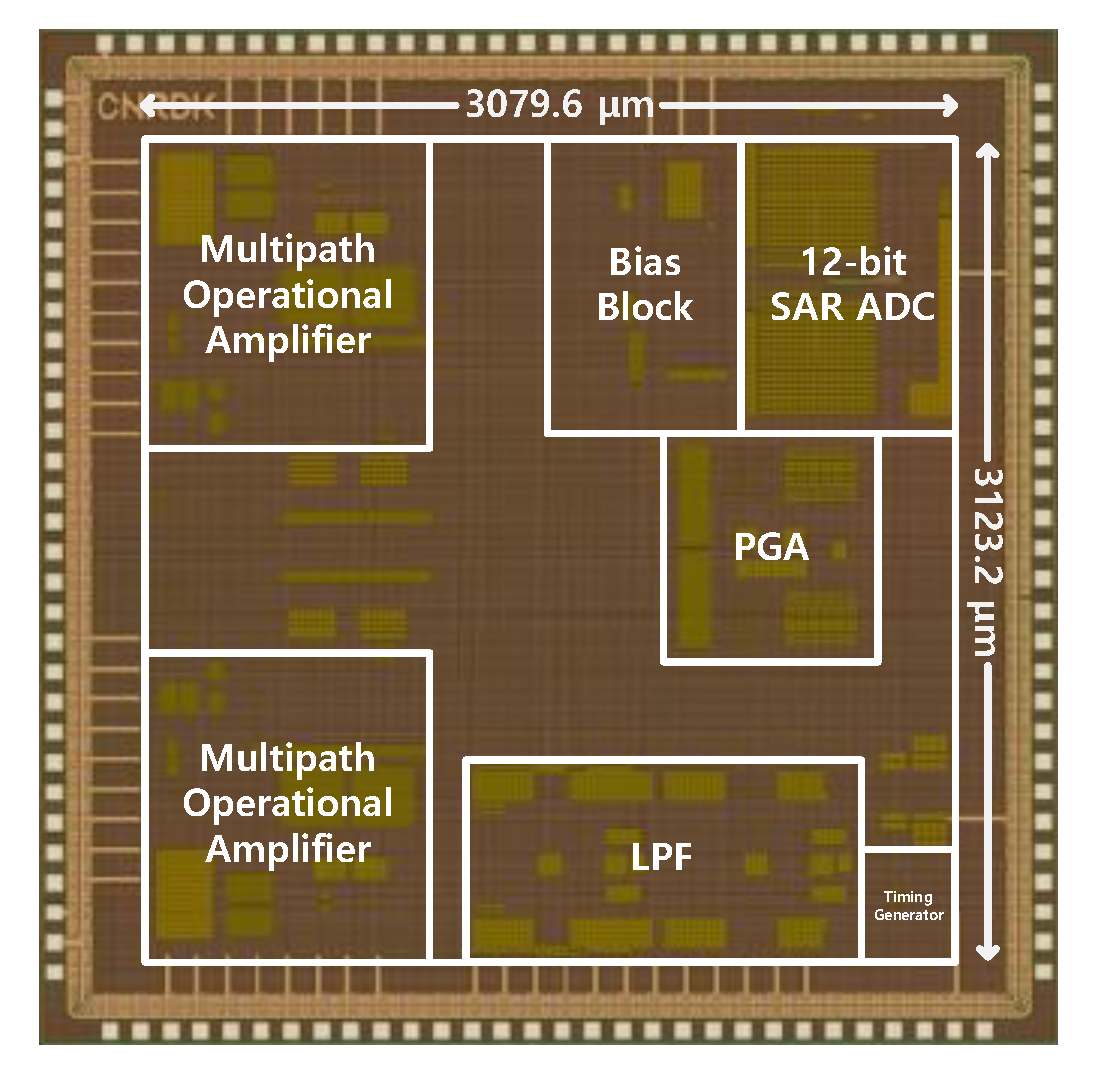
2.1. Top-Level Architecture

The block diagram of the proposed multimodal reconfigurable sensor readout circuit is shown in Figure 1. The proposed readout circuit uses a three-operational amplifier IA topology consisting of the reconfigurable structure, a programmable gain amplifier (PGA), and a low-pass filter (LPF). For digital processing, a 12-bit successive approximation register analog-to-digital converter (SAR ADC) was implemented.

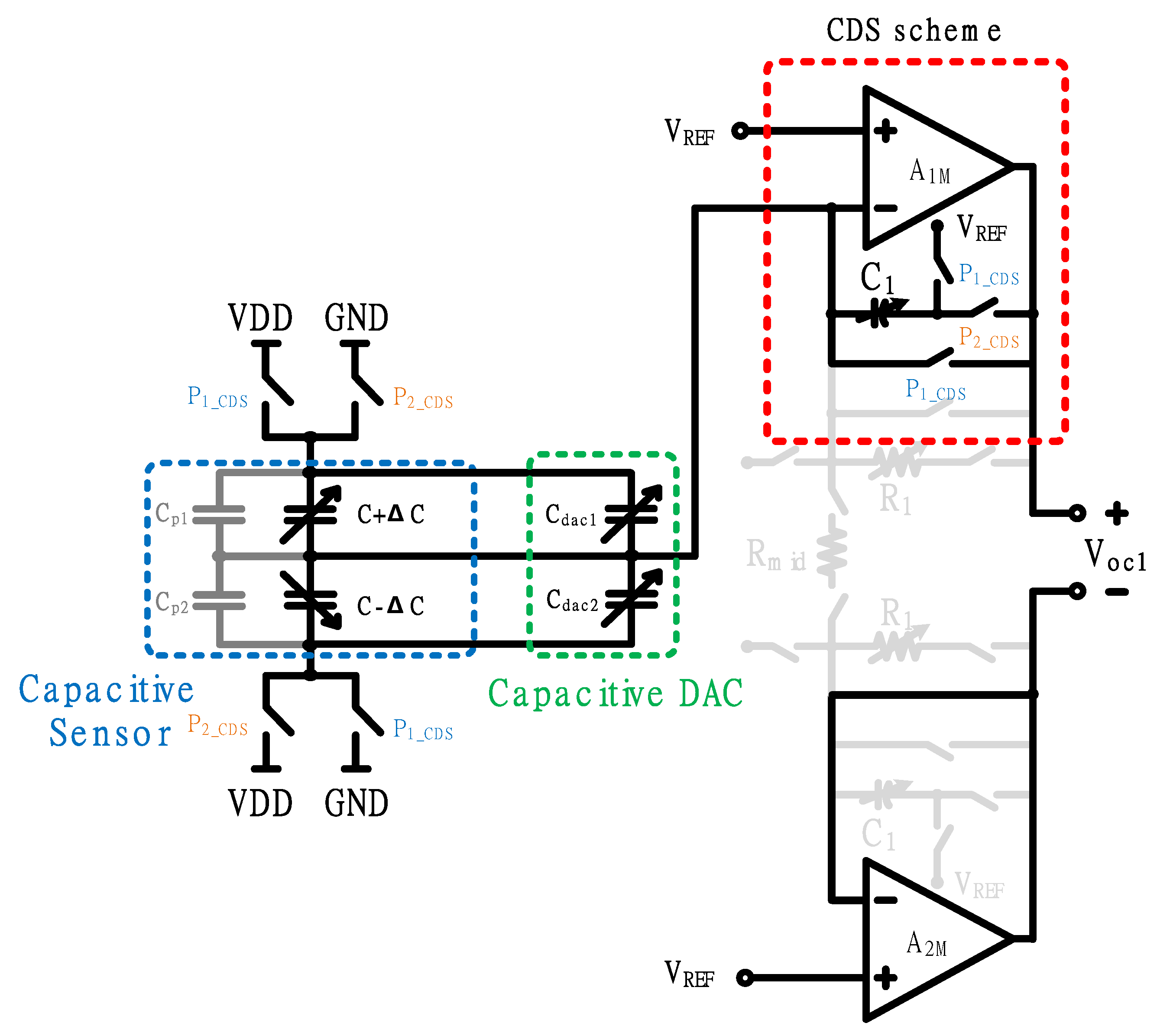
2.2. Reconfigurable Structure

The reconfigurable structure of the first stage according to the sensor application is shown in Figure 2 and Figure 3. Depending on the voltage/resistive-, current-, or capacitive-sensing modes, the chopper-stabilized, multi-path operational amplifiers, A1M and A2M can be reconfigured to three amplifier types: a voltage buffer, trans-impedance amplifier (TIA), and a CDS scheme. The reconfiguration of the amplifier is manually controlled by switches.
Figure 2 and Figure 3 illustrate the configurations of the possible sensing modes. To describe the readout operation, the sensor in the voltage/resistive-, current-, and capacitive-sensing modes in Figure 2 and Figure 3 is expressed by the resistive bridge, diode, and capacitive sensor, respectively.
The configuration of the voltage/resistive-sensing mode is shown in Figure 2a. The A1M and A2M amplifiers are converted to TIAs, which have a programmable feedback register R1. Rmid is connected to the negative input of the TIAs by switches such that the output signal is amplified by the ratio of R1 to Rmid. The output voltage of the voltage/resistive-sensing mode is expressed using the following equation:
V ov 1 = ( 1 + 2 R 1 R mid ) × V idv
The configurations of the current-sensing and capacitive-sensing modes are shown in Figure 2b and Figure 3 respectively. These configuration modes are available in both single-ended and differential modes. For simplicity, both modes are described using the single-ended mode. In the current-sensing mode configuration, the A1M amplifier is converted to a TIA and the A2M amplifier is converted to a voltage buffer. The output current of the sensor is converted into a voltage through the TIA. The ratio of the output voltage to the input current can be adjusted using programmable resistor R1, and is expressed using the following equation:
V oi 1 = R 1 × I in
In the capacitive-sensing mode configuration, the A1M amplifier is converted to the CDS scheme and the A2M amplifier reconfigures as a voltage buffer. In this mode, as the CDS scheme is operated by non-overlapping CDS clocks, P1CDS and P2CDS, the capacitive-sensing mode is driven under the discrete-time mode. If an offset exists in front of the A1M amplifier input, the CDS scheme can reduce the offset by subtracting the offset charges stored in capacitor C1 at the P1CDS and P2CDS clocks. Its output is amplified by the ratio of the input capacitance to a programmable capacitor C1, such that the output voltage is expressed using the following equation:
V oc 1 = V DD × 2 C C 1
In this mode, resolution degradation can be caused by the parasitic capacitance of the capacitive sensor. The parasitic capacitance is an unwanted component due to a process mismatch and random variations. The parasitic capacitance can often be greater than the change of input capacitance, resulting in a poor resolution. In extreme cases, the output voltage of the readout circuit can be ground or DC supply voltage. Assuming the capacitive sensor in Figure 3 has a parasitic capacitance, the output voltage is expressed using the following equation:
V oc 1 = V DD × ( 2 C + C p 1 C p 2 ) C 1
In the above equation, if Cp1 and Cp2 are ideally the same such that there is no effect on the output voltage. However, if Cp1 and Cp2 are different, and the difference of the value is large, Voc1 has an offset regardless of the input capacitance. To attenuate this difference, the 8-bit capacitive digital-to-analog converter (DAC) is applied. The Cdac1 and Cdac2, the capacitance of 8-bit capacitive DAC, can be adjusted from 0.1 pF to 12 pF to compensate for the difference in parasitic capacitances Cp1 and Cp2.
The CDS configuration of the PGA in the second stage is shown in Figure 4. The offset can be reduced by the CDS configuration of the second stage. If the amplifier operates in a capacitive-sensing mode, the offset can be reduced twice through two CDS configurations. The CDS operation of the PGA is driven by non-overlapping clocks, P1 and P2. In the P2 clock, the input and offset are stored in C2, and in the P1 clock, the offset stored in C2 is removed, such that a low offset can be achieved [18]. The input voltage of the PGA is amplified by the ratio of C2 to C3. The programmable capacitor C3 enables adjustment of the gain. The gain is expressed using the following equation:
V oPGA = C 2 C 3 × V ox 1
Consequently, the output voltages of the readout circuit according to the sensing mode (voltage/resistive-sensing mode, current-sensing mode, and capacitive-sensing mode) are respectively defined by the following equations:
V ovPGA = C 2 C 3 × ( 1 + 2 R 1 R mid ) × V idv
V oiPGA = C 2 C 3 × R 1 × I in
V ocPGA = C 2 C 3 × 2 C C 1 × V DD

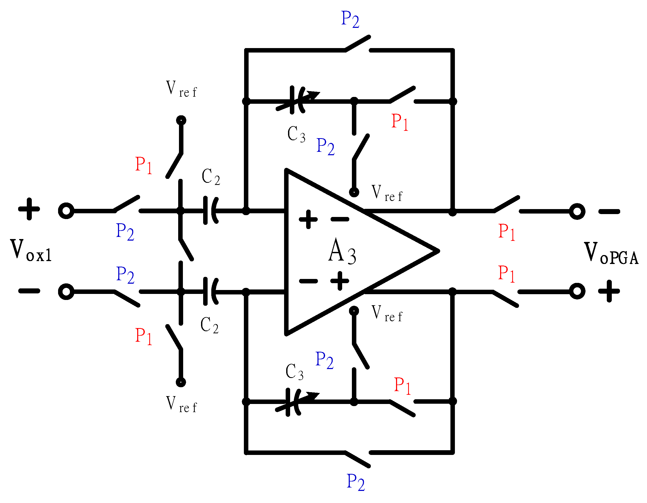
2.3. Detailed Description of the Amplifiers

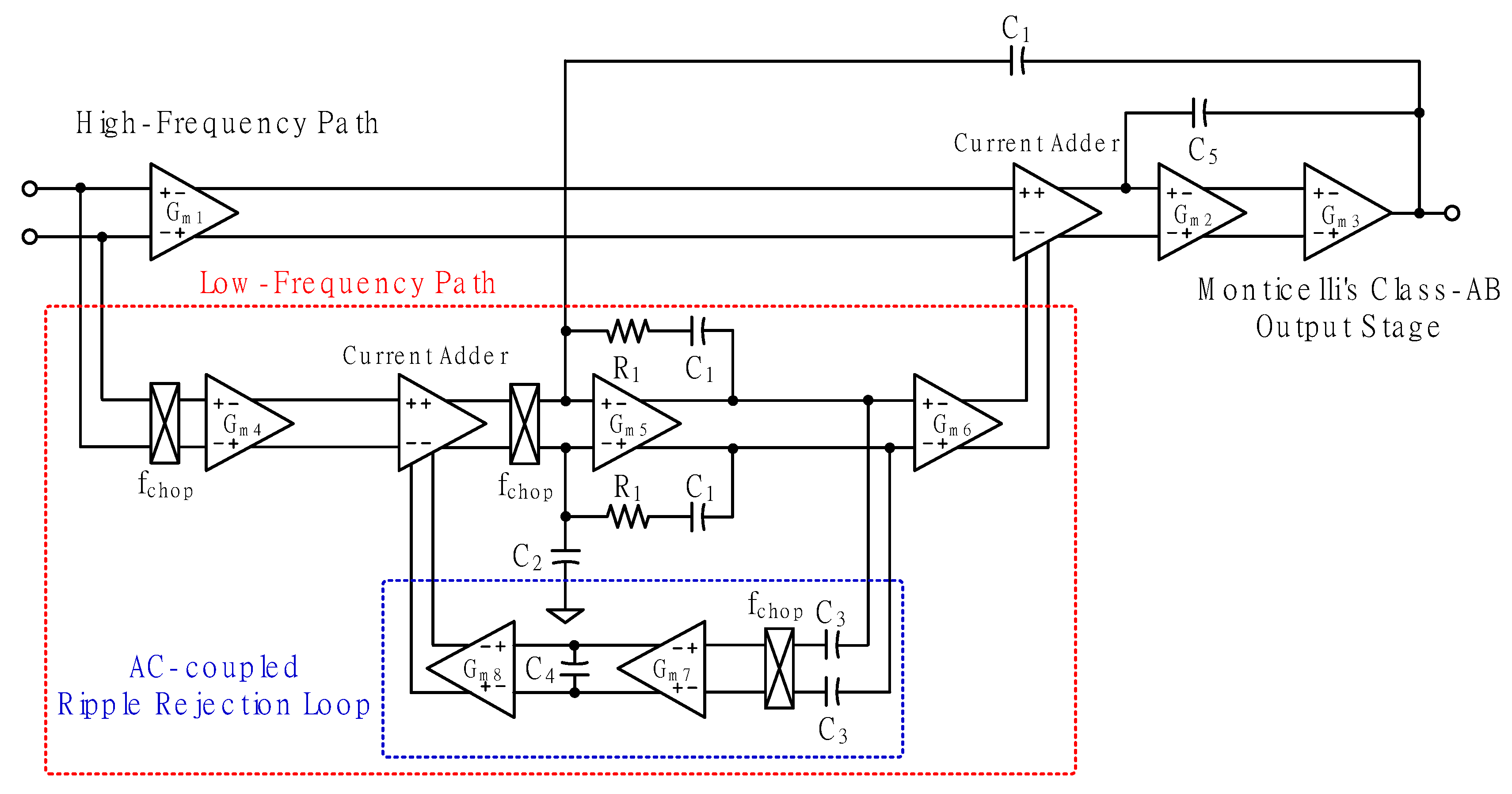
2.3.1. Chopper-Stabilized, Multi-Path Operational Amplifier with an AC-Coupled RRL

The block diagram of the chopper-stabilized, multi-path operational amplifier with an AC-coupled RRL is shown in Figure 5. This circuit has two main signal paths: a low-frequency path and a high-frequency path. The low-frequency path determines the gain and noise at low frequencies, while the high-frequency path determines the gain at high frequencies. This multi-path structure can compensate for the bandwidth limiting caused by chopper stabilization [17].
In the high-frequency path, the folded cascade stage is used to provide a high gain. A nested Miller compensation through C5 is applied for compensation in the high frequency path. To obtain a high power efficiency and slew rate, a Monticelli class-AB output stage was applied.
In the low-frequency path, the chopper stabilization technique was implemented to reduce the low-frequency noise. This technique modulates the low-frequency noise into the high-frequency band with low noise and then demodulates the input signal. It can reduce the low-frequency noise, but a ripple is generated, which can restrict the dynamic range of the amplifier. For a low supply voltage, the effects are more severe and should be reduced. To reduce the ripple, an AC-coupled RRL was applied. When the offset is at the input of the low-frequency path, the offset is up-modulated from DC to AC and amplified by Gm4. After entering the chopper circuit, the offset is demodulated from AC to DC and integrated in Gm5, causing a ripple approximated by the following equation:
V ripple V os G m 4 2 f chop C 2
The ripple enters the AC-coupled RRL through the capacitor C3 and the RRL reduces the ripple at Gm5 according to the following equation:
V rip _ RRL V os G m 4 2 G m 7 G m 8
By implementing the AC-coupled RRL, the ripple is reduced, but it causes a notch in the transfer function of the amplifier at the chopper frequency. This notch restricts the bandwidth of the amplifier. By combining the low-frequency path and high-frequency path signals in the current adder, the chopper-stabilized, multi-path structure can compensate for the notch caused by the AC-coupled RRL.

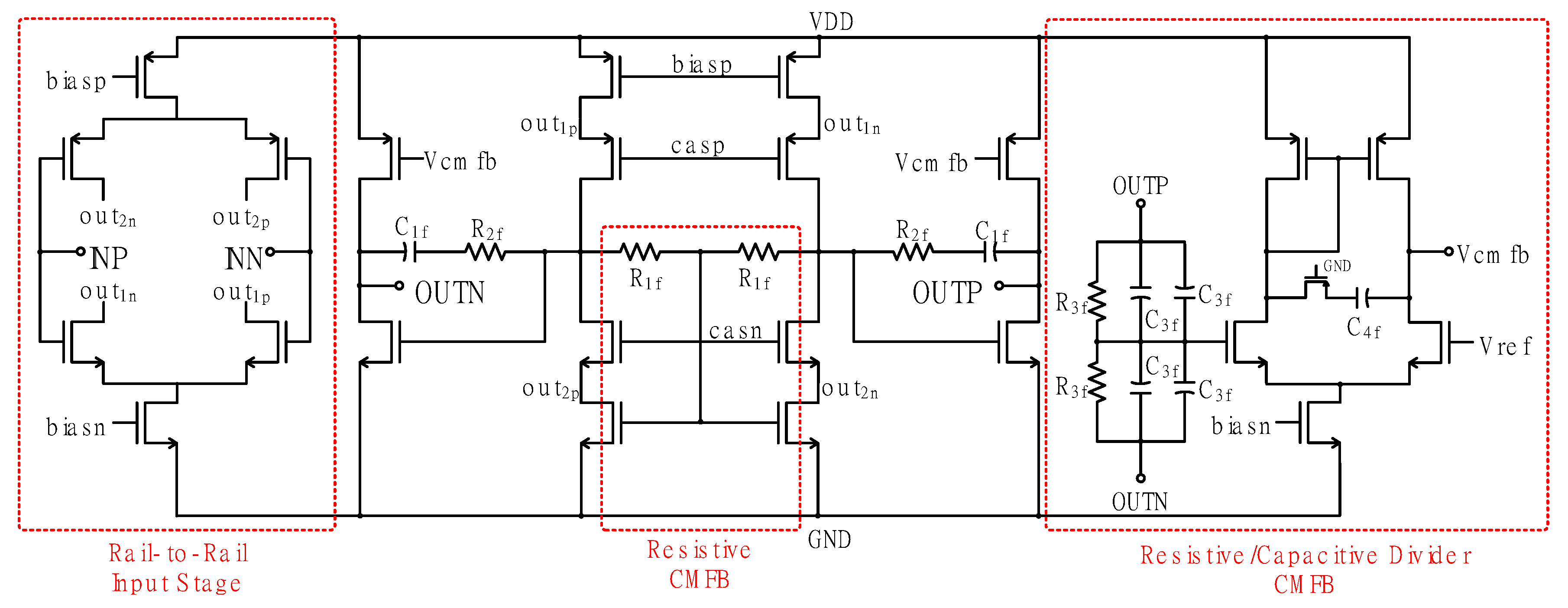
2.3.2. Fully Differential Amplifier

The fully differential amplifier with a rail-to-rail input stage in the PGA is shown in Figure 6. The rail-to-rail input stage can receive the output of the first stage over a wide range of values. To achieve a high gain, this amplifier has two stages: the folded cascade and common source (CS) stages [19]. To ensure frequency stability, the RC compensation using R2f and C1f is applied between the two stages.
In the amplifying stage, matching the common mode signal at the differential output is essential to obtain high signal-to-noise ratios, which is an advantage when using a differential pair. If the common mode signals of the differential outputs do not match each other, unnecessary components, including noise in the outputs, cannot be removed. In addition, the output dynamic range can be limited if common mode signals cannot be matched by the reference voltage, 0.9 V, in the CS stage. To solve this problem, the two common mode feedback (CMFB) scheme was applied. In the folded cascade stage, the resistive divider CMFB was applied. The output common mode signal, which is detected by the resistive divider, adjusts the current source consisting of an n-channel metal-oxide-semiconductor(NMOS). As the gate and drain of the NMOS form a negative feedback loop, the output common mode signal can be matched. In the CS stage, the CMFB consists of a resistive/capacitive divider and an error amplifier. The resistive/capacitive divider detects the common mode signal of the differential output at high and low frequencies. The error amplifier accepts the reference voltage and the detected common mode signal as a differential input and produces an output voltage, Vcmfb. Vcmfb is connected to the gate of the p-channel metal-oxide-semiconductor (PMOS) device in the CS stage, and a negative feedback loop is formed. The output common mode signal is matched to the reference voltage of 0.9 V by the negative feedback loop.

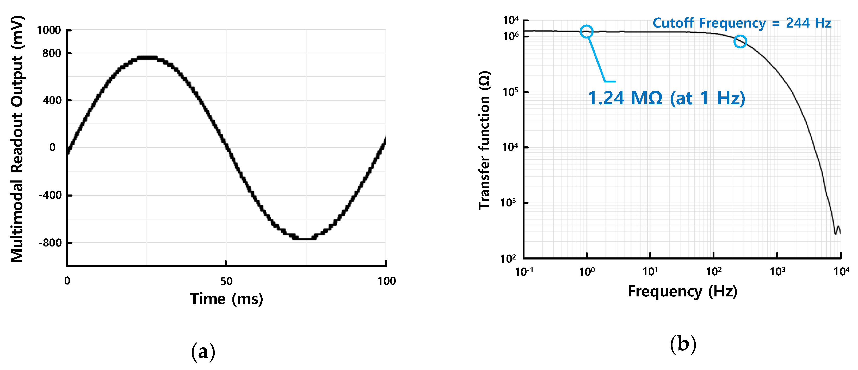
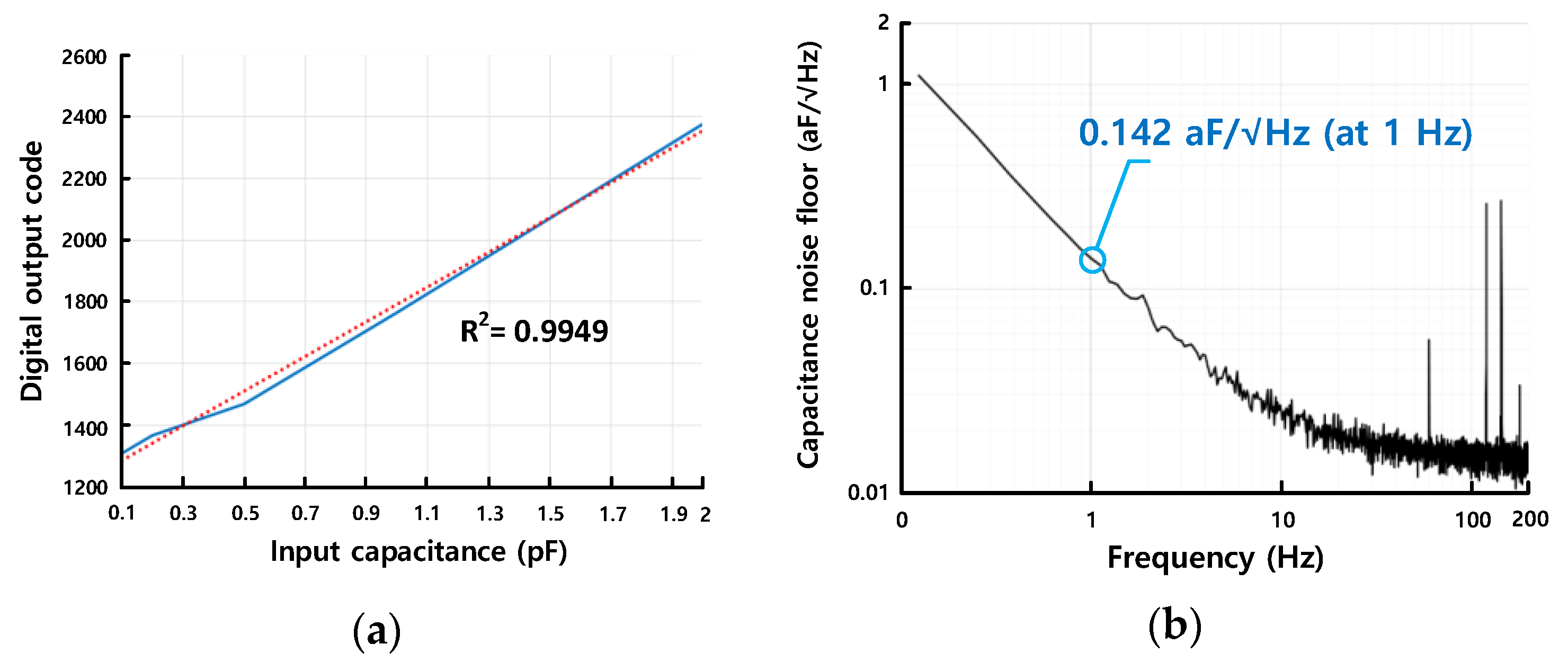
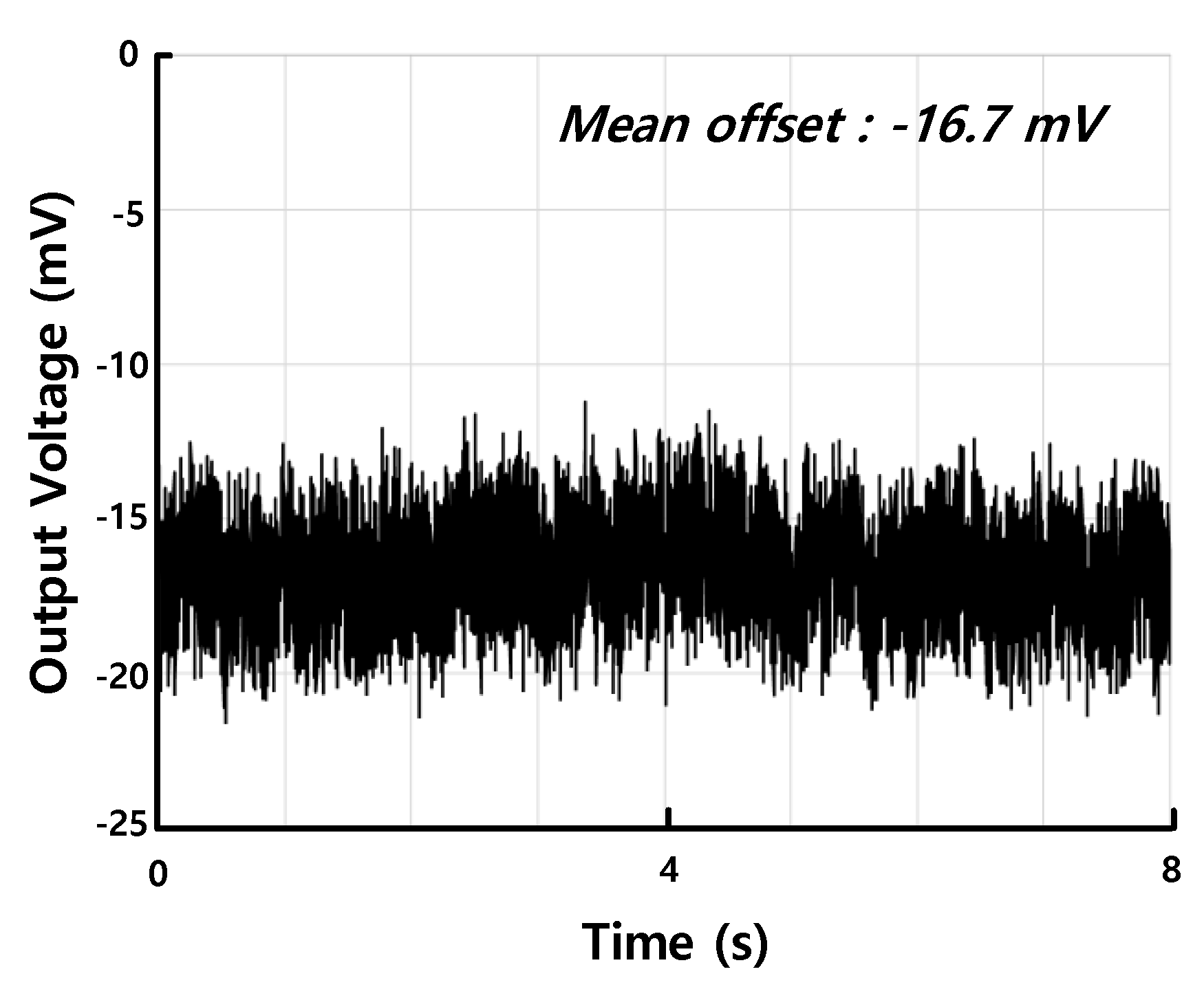
3. Measurement Results

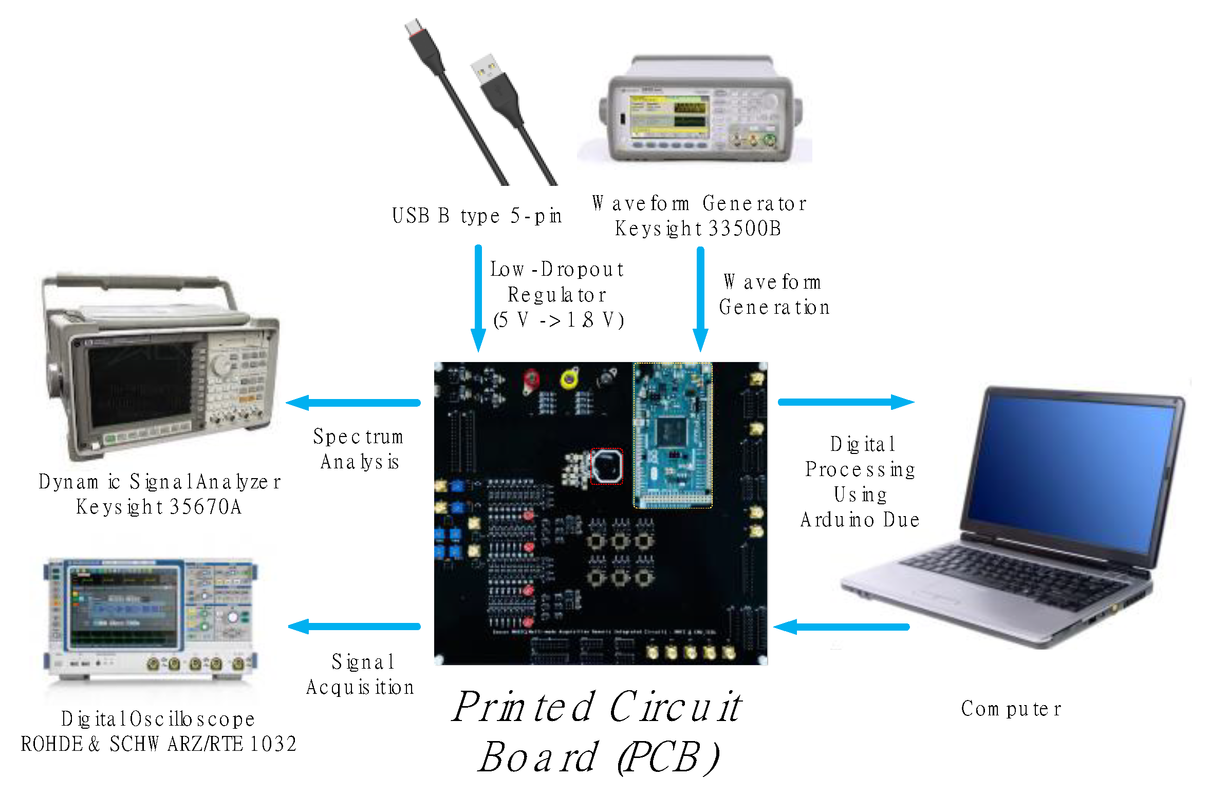
3.1. Measurement Results Using the Implemented Sensor on a Printed Circuit Board (PCB)

A photograph of the fabricated die is shown in Figure 7. The proposed readout circuit was fabricated using 0.18-µm complementary metal-oxide semiconductor (CMOS) technology. The active area of the fabricated die was 9.61 mm2. The measurement setup is shown in Figure 8. For measurement devices, Keysight’s 35670A was used for spectrum analysis, Rohde & Schwars’s RTE 1032 was used for signal acquisition, and Keysight’s 33500B was used for waveform generation. Arduino’s Arduino Due microcontroller was mounted on a PCB for the digital processing of analog output signals and was directly connected to the digital output of the ADC. In the voltage-sensing mode, the gain could be adjusted from 26 dB to 55 dB by fixing the PGA gain to 13.9 dB. The gain of the PGA was also adjustable from 13.9 dB to 44 dB. The output voltage in the voltage-sensing mode is shown in Figure 9a. The transfer function in the voltage-sensing mode is shown in Figure 9b. A DC gain of 37.4 dB was measured, and the cut-off frequency was 182 Hz. The measured input referred noise in the voltage-sensing mode is shown in Figure 10. The measured input referred noise at 1 Hz was 2.09 µV/√Hz. The RMS input referred noise was calculated to be 5.25 µVrms over the bandwidth from 1 Hz to 200 Hz.
In the resistive-sensing mode, the gain, which is the ratio of the output voltage to the input voltage, equals the gain of the voltage-sensing mode because the resistive-sensing mode shares the configuration of the voltage-sensing mode. The linearity expressed by the ratio of the digital output code to the input resistance is shown in Figure 11a. The coefficient of determination, R2, was calculated to be 0.9991. The resistance noise floor is shown in Figure 11b. The resistance noise floor was calculated by dividing the input referred noise by 180 mV/kΩ, which was the ratio of the input voltage to the input resistance. This ratio was calculated using a bridge sensor consisting of four 10 kΩ resistors. The resistance noise floor at 1 Hz was 1.16 mΩ/√Hz. The RMS resistance noise floor was calculated to be 2.9 mΩrms over the bandwidth from 1 Hz to 200 Hz.
In the current-sensing mode, the gain, which is the ratio of output voltage to the input current, could be adjusted from 0.544 MΩ to 11.5 MΩ by fixing the PGA gain to 13.9 dB. The output in the current-sensing mode is shown in Figure 12a. The transfer function of the current-sensing mode is shown in Figure 12b. The DC gain was measured to be 1.24 MΩ and the cut-off frequency was 244 Hz. The measured input referred current noise is shown in Figure 13. The measured input referred current noise at 1 Hz was 25.5 pA/√Hz. The RMS input current noise was 742 pArms over the bandwidth from 1 Hz to 200 Hz. In the capacitive-sensing mode, the linearity expressed by the ratio of the digital output code to the input capacitance, is shown in Figure 14a. The coefficient of determination, R2, was calculated to be 0.9949. The measured capacitance noise floor is shown in Figure 14b. The capacitance noise floor was measured by dividing the gain by the output noise density, which is the ratio of output voltage to the input capacitance. The gain of the capacitive-sensing mode is expressed by the following equation:
Gain = V DD C 1 ( 1 st   stage   gain ) × ( 2 nd   stage   gain ) = 1.8   V 1.84   pF × 36.8   pF 0.23   pF = 156   mV / fF
The gain could be adjusted from 250 mV/pF to 1250 mV/fF. The measured capacitance noise floor at 1 Hz was 0.142 aF/√Hz. The RMS capacitance noise floor was 0.313 aFrms over the bandwidth from 1 Hz to 200 Hz.
In the capacitive-sensing-mode test, the capacitive DAC inside the chip was tuned to reduce the offset due to the parasitic capacitance. For the capacitive inputs, the difference due to the input parasitic capacitance had a value of 2.67 pF caused by the PCB and the capacitive sensor. After adjustment, the difference due to the input parasitic capacitance was 0.09 pF. The measured offset voltage of the capacitive-sensing mode after adjustment is shown in Figure 15.
The performance summary of proposed multimodal readout circuit is shown in Table 1.

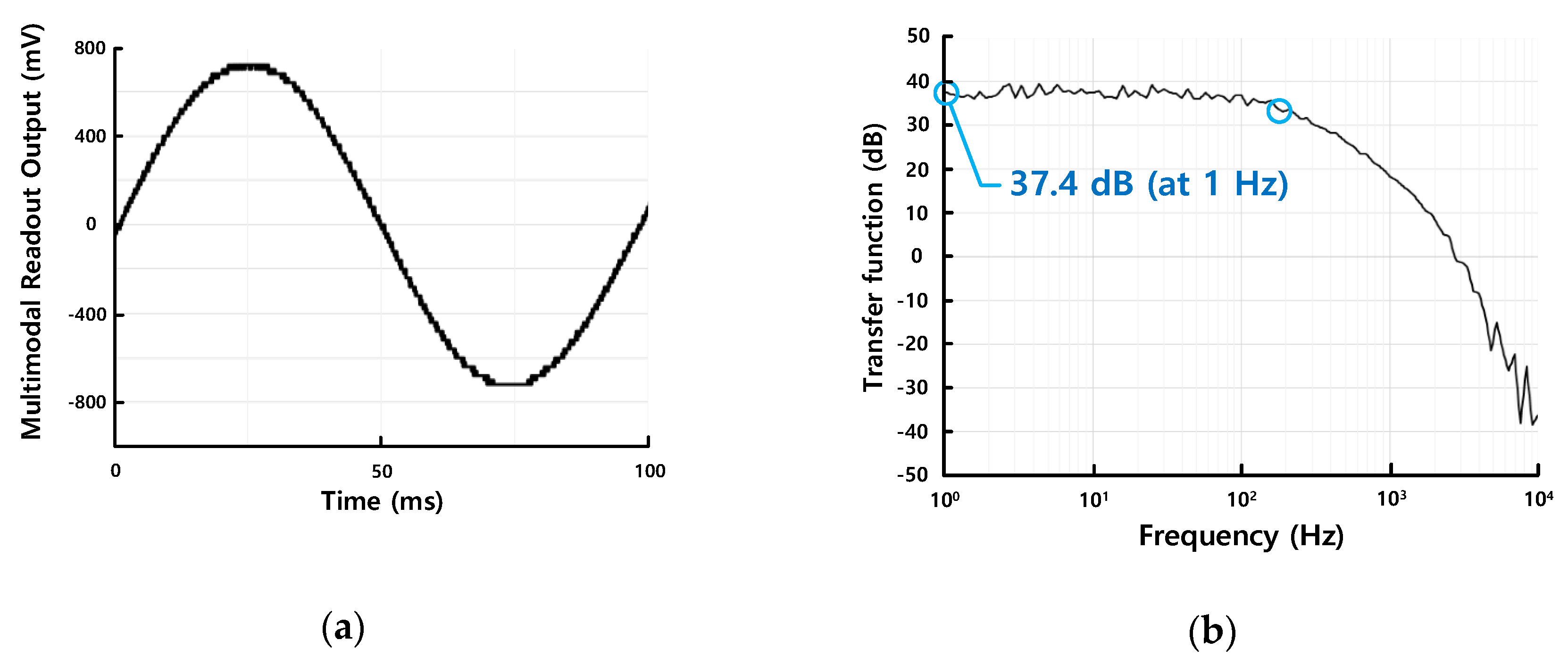
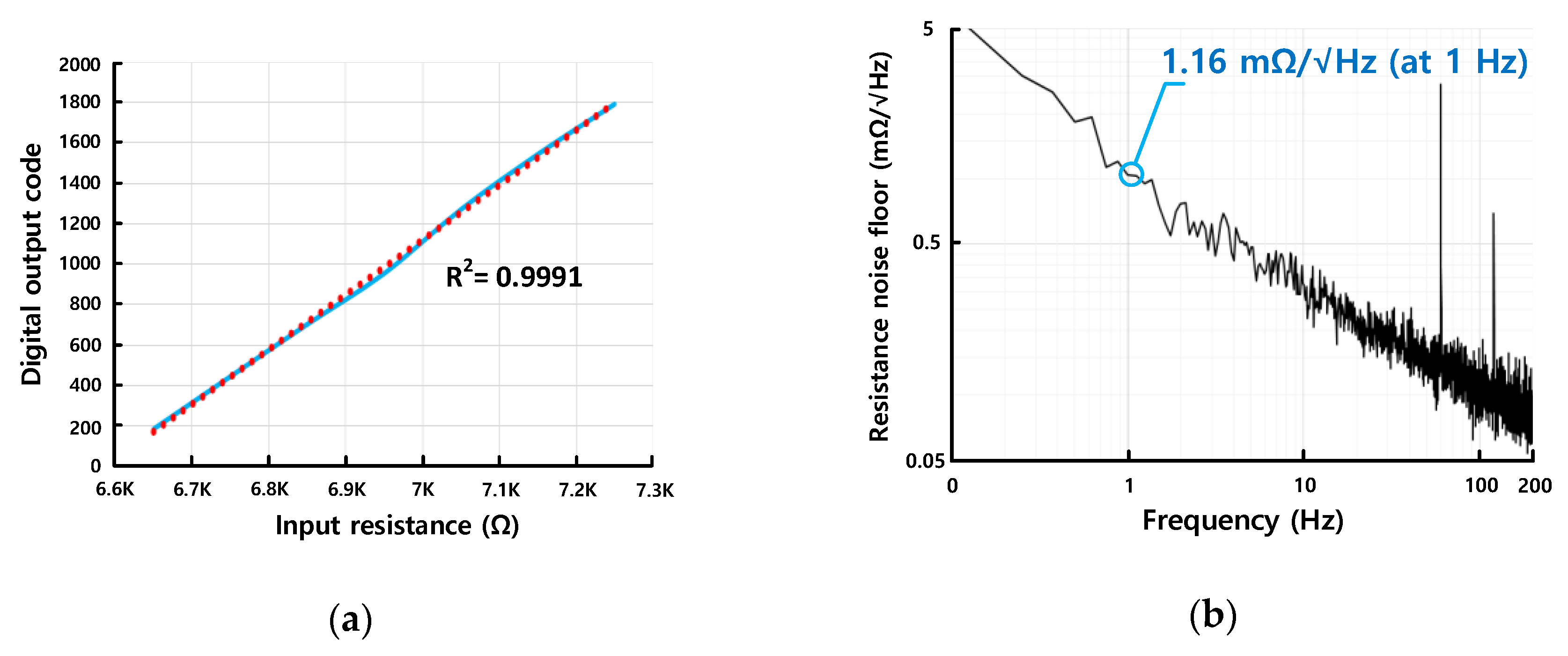
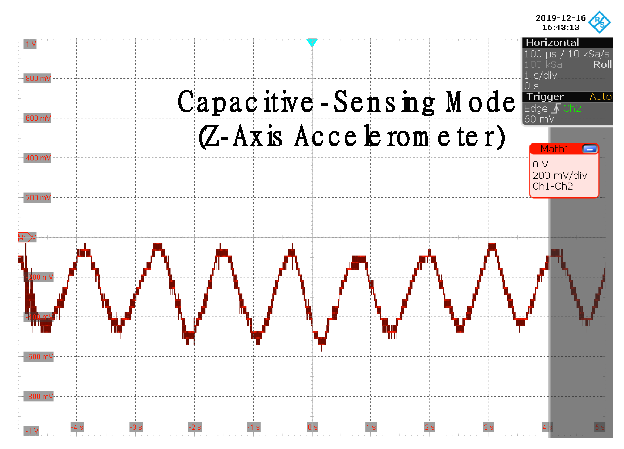
3.2. Measurement Results Using a Real Application

For a resistive/capacitive-sensing-mode test using a real application, a flexible bend sensor, which senses a bending force via a change of resistance and a capacitive z-axis accelerometer, were used. Each sensor specification is shown in Table 2.
The photography of sensors on the PCB are shown in Figure 16. The real-time measurement result using a flexible bend sensor and a z-axis accelerometer are shown in Figure 17 and Figure 18, respectively. In Figure 17, in resistive-sensing mode, the resistive bridge sensor including a flexible bend sensor was applied. The resistive bridge sensor was constructed using three variable 10 kΩ resistors and a flexible bending sensor. Also, the gain of the readout circuit was adjusted to 26 dB. The degree of bending was adjusted in consideration of the bend resistance range of the sensor and the input resistance range of the designed readout circuit. The output amplitude of the readout circuit was measured up to 860 mV, which was approximately 400 Ω in terms of resistance.
In Figure 18, in capacitive-sensing mode, the parasitic capacitance was reduced by using an 8-bit capacitive DAC inside the chip after considering the input parasitic capacitance inside the sensor. Also, the gain was adjusted to 4 mV/fF. The amplitude of the output of the readout was measured in the range of 400–450 mV, which was a variation of about from 0.1 pF to 0.12 pF. Considering the specification of the z-axis accelerometer sensor, the acceleration was about 0.8 g to 0.96 g.
The performance summary and comparison with references is shown in Table 3.

4. Conclusions

A low-noise multimodal reconfigurable sensor readout circuit for voltage/resistive/current/capacitive microsensors has been presented. The proposed circuit has a reconfigurable structure that can provide a voltage/resistive-sensing mode, a current-sensing mode, or a capacitive-sensing mode. The reconfigurable characteristics of the proposed circuit can be applied in an environmental monitoring system using various sensors. A low noise and wide bandwidth were achieved by applying multiple DOC techniques, including chopper stabilization and the CDS technique. The chopper-stabilized, multipath operational amplifier with an AC-coupled RRL resolved the band-limiting issue and the ripple caused by the chopper. The measurement input noise values in the voltage/resistive/current/capacitive-sensing modes were 5.25 µVrms, 2.9 mΩrms, 742 pArms, and 0.313 aFrms, respectively, from 1 Hz to 200 Hz. The proposed readout circuit was fabricated using 0.18-µm CMOS technology to fabricate a device with an active area of 9.61 mm2. The total power consumption was 2.552 mW with a 1.8-V supply voltage.

Author Contributions

Conceptualization and supervision, H.K. (Hyoungho Ko); investigation and writing—original draft preparation, D.Y.; writing—review and editing, H.K. (Hyungseup Kim), J.K., K.H., H.H., Y.K., G.K., W.S.S., J.W.L. and B.J.L. All authors have read and agreed to the published version of the manuscript.

Funding

This research was supported by the NanoMaterial Technology Development Program through the National Research Foundation of Korea (NRF) funded by the Ministry of Science and ICT (NRF-2015M3A7B7045527). This research was also supported by the Brain Korea 21 Plus Project.

Acknowledgments

The chip fabrication and EDA tool were provided by the IC Design Education Center (IDEC), Korea.

Conflicts of Interest

The authors declare no conflicts of interest.

References

  1. Chen, S.; Xu, H.; Liu, D.; Hu, B.; Wang, H. A Vision of IoT: Applications, Challenges, and Opportunities with China Perspective. IEEE Internet Things J. 2014, 1, 349–359. [Google Scholar] [CrossRef]
  2. Alhoshany, A.; Omran, H.; Salama, K.N. A 45.8 fJ/Step, energy-efficient, differential SAR capacitance-to-digital converter for capacitive pressure sensing. Sens. Actuators Phys. 2016, 245, 10–18. [Google Scholar] [CrossRef]
  3. Gómez-Ramírez, E.; Maeda-Nunez, L.A.; Álvarez-Simón, L.C.; Flores-García, F.G. A Highly Robust Interface Circuit for Resistive Sensors. Electronics 2019, 8, 263. [Google Scholar] [CrossRef] [Green Version]
  4. Song, H.; Park, Y.; Kim, H.; Cho, D.D.; Ko, H. Fully integrated low-noise readout circuit with automatic offset cancellation loop for capacitive microsensors. Sensors 2015, 15, 26009–26017. [Google Scholar] [CrossRef] [PubMed] [Green Version]
  5. Lee, B.; Kim, H.; Kim, J.; Han, K.; Shin, S.; Kim, G.; Sul, W.S.; Lee, B.J.; Lee, S.; Ko, H. Low-noise 16-bit First-order Delta-sigma Capacitance-to-digital Converter for Capacitive Humidity Sensor. Sens. Mater. 2019, 31, 1523–1533. [Google Scholar] [CrossRef]
  6. Mun, Y.; Kim, H.; Ko, Y.; Park, Y.; Koo, K.; Cho, D.D.; Ko, H. Capacitive analog front-end circuit with dual-mode automatic parasitic cancellation loop. Microsyst. Technol. 2017, 23, 515–523. [Google Scholar] [CrossRef]
  7. Omran, H.; Arsalan, M.; Salama, K.N. An integrated energy-efficient capacitive sensor digital interface circuit. Sens. Actuators Phys. 2014, 216, 43–51. [Google Scholar] [CrossRef]
  8. Shah, J.; Mishra, B. IoT enabled Environmental Monitoring System for Smart Cities. In Proceedings of the 2016 Internet of Things and Applications (IOTA), Pune, India, 22–24 January 2016. [Google Scholar]
  9. Park, K.; Kim, S.; Eom, W.; Kim, J. A Reconfigurable Readout Integrated Circuit for Heterogeneous Display-Based Multi-Sensor Systems. Sensors 2017, 17, 759. [Google Scholar] [CrossRef] [PubMed] [Green Version]
  10. Helleputte, N.K.; Konijnenburg, M.K.; Kim, H.; Pettine, J.; Jee, D.; Breeschoten, A.; Morgado, A.; Torfs, T.; Groot, D.H.; Hoof, C.V.; et al. 18.3 A multi-parameter signal-acquisition SoC for connected personal health applications. In Proceedings of the 2014 IEEE International Solid-State Circuits Conference Digest of Technical Papers (ISSCC), San Francisco, CA, USA, 9–13 February 2014. [Google Scholar]
  11. Musa, A.; Minotani, T.; Matsunaga, K.; Kondo, T.; Morimura, H. An 8-Mode Reconfigurable Sensor-Independent Readout Circuit for Trillion Sensors Era. In Proceedings of the 2015 IEEE Tenth International Conference on Intelligent Sensors, Sensor Networks and Information Processing (ISSNIP), Singapore, 7–9 April 2015. [Google Scholar]
  12. Huang, Y.; Tzeng, T.; Lin, T.; Huang, C.; Yen, P.; Kuo, P.; Lin, C.; Lu, S. A Self-Powered CMOS Reconfigurable Multi-Sensor SoC for Biomedical Applications. IEEE J. Solid State Circuit 2014, 49, 851–866. [Google Scholar] [CrossRef]
  13. Ghoreishzadeh, S.; Boero, C.; Pullini, A.; Baj-Rossi, C.; Carrara, S.; Micheli, G. Sub-mW Reconfigurable Interface IC for Electrochemical Sensing. In Proceedings of the 2014 IEEE Biomedical Circuits and Systems Conference (BioCAS) Proceedings, Lausanne, Switzerland, 22–24 October 2014. [Google Scholar]
  14. Jun, J.; Rhee, C.; Kim, M.; Kang, J.; Kim, S. A 21.8 b sub-100μHz 1/f corner 2.4 μV-offset programmable-gain read-out IC for bridge measurement systems. In Proceedings of the 2018 IEEE International Solid—State Circuits Conference (ISSCC), San Francisco, CA, USA, 11–15 February 2018. [Google Scholar]
  15. Belloni, M.; Bonizzoni, E.; Fornasari, A.; Maloberti, F. A Micropower Chopper—CDS Operational Amplifier. IEEE J. Solid State Circuits 2010, 45, 2521–2529. [Google Scholar] [CrossRef]
  16. Lee, B.; Ko, Y.; Kim, H.; Mun, Y.; Huh, S.; Song, D.; Roh, Y.; Ko, H. Low-noise Reconfigurable 12- to 16-bit Delta-Sigma Capacitance-to-digital Converter with Chopper Stabilization Technique. Sens. Mater. 2018, 30, 1671–1679. [Google Scholar] [CrossRef]
  17. Ko, H.; Kim, H.; Lee, B.; Kim, J.; Cho, D.D.; Han, K. Low-noise Analog Front-end with Chopper-stabilized Multipath Current-feedback Instrumentation Amplifier for Resistive Sensors. Sens. Mater. 2019, 30, 1697–1706. [Google Scholar] [CrossRef]
  18. Enz, C.C.; Temes, G.C. Circuit techniques for reducing the effects of op-amp imperfections: Autozeroing, correlated double sampling, and chopper stabilization. Proc. IEEE 1996, 84, 1584–1614. [Google Scholar] [CrossRef] [Green Version]
  19. Mallya, S.; Nevin, J.H. Design procedures for a fully differential folded-cascode CMOS operational amplifier. IEEE J. Solid State Circuits 1989, 24, 1737–1740. [Google Scholar] [CrossRef]
  20. Ong, G.T.; Chan, P.K. A Power-Aware Chopper-Stabilized Instrumentation Amplifier for Resistive Wheatstone Brdige Sensors. IEEE Trans. Instrum. Meas. 2017, 63, 2253–2264. [Google Scholar] [CrossRef]
  21. Zhao, M.; Lu, W.; Chen, Z.; Zhang, T.; Wu, F.; Zhang, Y.; Liu, D. A Low-Noise Switched-Capacitor Interface for a Capacitive Micro-Accelerometer. In Proceedings of the 2015 IEEE International Symposium on Circuits and Systems (ISCAS), Lisbon, Portugal, 24–27 May 2015. [Google Scholar]
Figure 1. Block diagram of the proposed multimodal reconfigurable sensor readout circuit. ADC: analog-to-digital converter, LPF: low-pass filter.
Applsci 10 00348 g001
Figure 2. (a) Configuration of the voltage/resistive-sensing mode (b) Configuration of the current-sensing mode. GND: ground, VDD: dc supply voltage.
Applsci 10 00348 g002
Figure 3. Configuration of the capacitive-sensing mode. CDS: correlated double sampling, DAC: digital-to-analog converter.
Applsci 10 00348 g003
Figure 4. CDS configuration of the programmable gain amplifier (PGA) in the second stage.
Applsci 10 00348 g004
Figure 5. Block diagram of the chopper-stabilized, multi-path operational amplifier with an AC-coupled RRL.
Applsci 10 00348 g005
Figure 6. Fully differential amplifier with rail to rail input stage in the PGA. CMFB: common mode feedback, INN: negative input, INP: positive input, OUTN: negative output, OUTP: positive output.
Applsci 10 00348 g006
Figure 7. Photograph of the fabricated die, SAR: successive approximation register.
Applsci 10 00348 g007
Figure 8. Measurement setup for the proposed readout circuit.
Applsci 10 00348 g008
Figure 9. (a) Output in the voltage-sensing mode. (b) Transfer function in the voltage-sensing mode.
Applsci 10 00348 g009
Figure 10. Measured input referred noise in the voltage-sensing mode.
Applsci 10 00348 g010
Figure 11. (a) Linearity expressed as the ratio of the digital output code to the input resistance. (b) Resistance noise floor.
Applsci 10 00348 g011
Figure 12. (a) Output in the current-sensing mode. (b) Transfer function of the current-sensing mode.
Applsci 10 00348 g012
Figure 13. Measured input referred current noise in the current-sensing mode.
Applsci 10 00348 g013
Figure 14. (a) Linearity expressed as the ratio of the digital output code to the input capacitance. (b) Capacitance noise floor.
Applsci 10 00348 g014
Figure 15. The measured offset voltage of the capacitive-sensing mode after adjustment.
Applsci 10 00348 g015
Figure 16. (a) Photograph of the flexible bend sensor on a PCB. (b) Photograph of a z-axis accelerometer on a PCB.
Applsci 10 00348 g016
Figure 17. The real-time measurement result using a flexible bend sensor.
Applsci 10 00348 g017
Figure 18. The real-time measurement result using a capacitive z-axis accelerometer.
Applsci 10 00348 g018
Table 1. Performance summary. CMOS: complementary metal-oxide semiconductor, UGBW: unit gain bandwidth.
Overall Performance of the Proposed Multimodal Readout Circuit
Technology1P6M 0.18-µm CMOS Process
Supply Voltage1.8 V
Multimodal Readout CircuitBias Block
Signal typeVoltageResistanceCurrentCapacitancePower483.7 µW (sim)
Low-Pass Filter
Input range70 mV (max)0.4–400 Ω1.65 µA
(max)
±2 pFBandwidth1 kHz (sim)
Total power2.784 mW2.552 mW2.8 mWPower487.8 µW (sim)
Input noise
(1–200 Hz)
5.25 µVrms2.9 mΩrms742 pArms0.313 aFrmsPGA
Pchop1 MHz (chopping frequency)Gain13.9–44 dB
Pcds125 kHz (CDS frequency)Power608 µW (sim)
Multi-Path Operational AmplifierClock Generator
Power10.09 µW (sim)Power138 µW (sim)
UGBW4.81 MHz
Open loop gain98 dB
12-bit SAR ADC
Power802.98 µW (sim)
Sampling frequency1 MHz
Table 2. Sensor specification.
Flexible Bend SensorCapacitive Z-Axis Accelerometer
Signal TypeRSignal TypeC
Flat resistance10 kΩTorque/g2.03 × 10−10
Resistance tolerance±30%Nominal capacitance5.409 pF
Bend resistance range60–110 kΩΔ C/g0.125 pF/g
Resolution0.5 mg
Δ degree/g 3.65 × 10⁻⁴ μm/g
Table 3. Performance summary and comparison.
ParameterThis WorkRef. [20]Ref. [21]Ref. [10]Ref. [12]
Supply (V)1.82.751.21.8
Technology (µm)0.180.180.350.180.35
Power consumption (mW)2.5520.02765189.30.0580.942
Area (mm2)9.61N/A12.5N/A11.25
Signal typeV/I/R/CRCV/RV/I/R/C
Noise cancellationChopping, CDSChoppingCDSChoppingChopping
Input noise5.25 µVrms3.76 µVrmsN/A0.6 µVrms0.769 µVrms
Resistance noise floor2.9 mΩrmsN/AN/A8.6 mΩ/√HzN/A
Input current noise742 pArmsN/AN/AN/AN/A
Capacitance noise floor0.313 aFrmsN/A0.41 aFrmsN/AN/A
Input rangeV: 70 mVpp
R: 0.4–400 Ω
I: 1.65 µA
C: ±2 pF
V: 17.6 mVC: ±2.9 pFV: 30 mVpp
R: N/A
C: 10 pF

