1. Introduction
The new industries in various fields are in the spotlight with the introduction of the new industrial era. One of them is the next generation material development industry. Carbon material is greatly popular and a promising material among existing materials, and is able to be used in various fields such as displays, electron application devices, wearable devices, batteries and renewable energy [
1,
2,
3,
4]. Typical carbon materials include graphene, carbon nanotube (CNT), diamond-like carbon (DLC), carbon black and fullerene. Graphene and CNTs have outstanding electrical, mechanical, thermal, and flexibility properties, and with various studies that have been conducted, they have reached the step before commercialization of the application industry. In addition to these, the carbon nanowall (CNW) is a material that has unlimited potential. CNW has many advantages with carbon allotrope, like the materials mentioned above. CNW, with its multi-layer graphenes standing perpendicular to the substrate, has the largest surface area of any carbon allotrope [
5]. CNW is actively used in application sensors because the large surface area can be applied as a great advantage in application devices such as sensors. Especially, in the case of a sensor adopted with the electrochemical mechanism, it can be a great advantage [
6]. However, CNW has many porous-like air gaps on its surface, so its electrical properties are poor compared to graphene and CNT. CNW also has a buffer layer for nucleation and graphene layer growth. This buffer layer is an amorphous carbon layer [
7]. The material, having a general amorphous structure, does not have remarkable electrical properties because of the non-crystallization and non-orientation. In order to alleviate these disadvantages, various experiments have been conducted to improve the surface and electrical properties of CNW. Improvements in properties through pre-treatment and post-treatment are typical, and there are various methods such as utilizing metal-based particles or doping gaseous gases.
In this experiment, the electrical properties were improved by using MWCNT (multi-walled carbon nanotube) as the buffer layer of a carbon nanowall. After forming a buffer layer with different CNT contents, CNW was synthesized by chemical vapor deposition. Thereafter, a lot of electrical characteristics were analyzed and compared with the general CNW.
2. Experimental
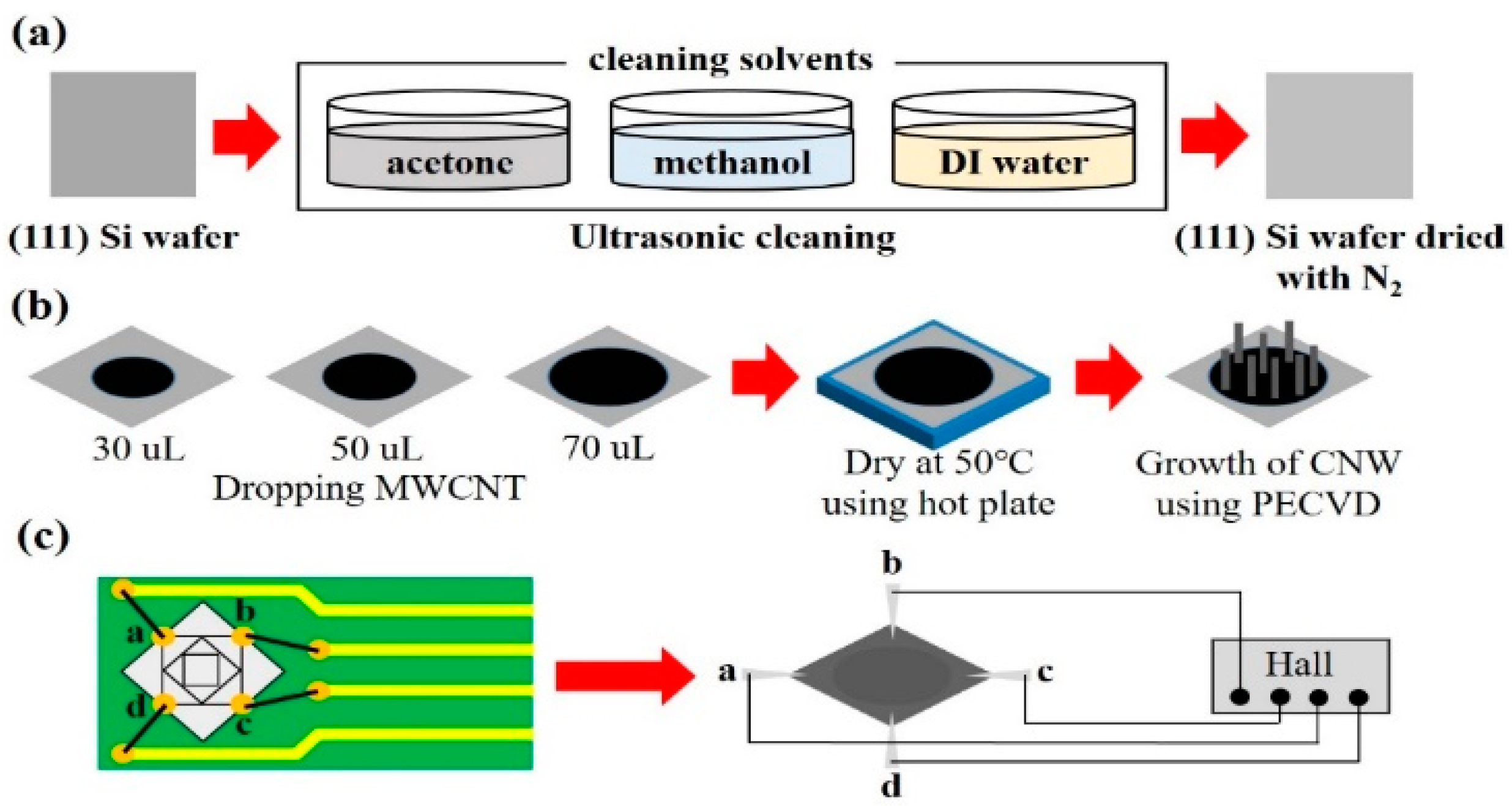
Si wafers with (111) orientation were soaked in acetone and ultrasonically cleaned for 15 min. After, acetone-treated Si wafers were immediately put into methanol and cleaned for 10 min to blow off the surface acetone components. The final washing and drying were performed using DI pure water and N2 gas. Then, MWCNT dispersed in water (US Research Nanomaterials, Inc., Houston, TX, USA, 4 science) having an outside diameter of 5–15 nm and length of 50 µm was used to form a MWCNT-based buffer layer on the prepared Si wafer, and detailed specifications of MWCNT are shown in
Table 1. The amount of MWCNTs used for the formation of the buffer layer was adjusted to 30, 50, and 70 µL, and dropped on a Si wafer, followed by drying at 50 °C for 1 h using a hot plate. The CNW was grown on a MWCNT-based buffer layer using microwave PECVD. The growth conditions of CNW are 1300 W (microwave power), growth time (10 min), 700 °C (substrate temperature), gas ratio (H
2: 25 sccm and CH
4: 50 sccm), 2.5 × 10
−2 torr (working pressure). The various analyses were operated to investigate the characteristics of CNW grown on a MWCNT-based buffer layer. FE-SEM (field emission scanning electron microscopy, Hitachi-S4800) was operated for surface and cross section analysis under acceleration voltage (10~15 kV), emission current (8600 nA), and lens mode (high). Raman spectra (FEX MRA10, NOST) analysis was performed to examine the successful growth of CNW and structural changes caused by the MWCNT-based buffer layer under conditions such as excitation laser wavelength (~531 nm), excitation laser power (~0.30 mW), objective lens (50×) and spectral resolution (1.87–2.89 cm
−1). The hall measurement system (HMS-3000, Ecopia) analysis was conducted to observe the electrical characteristics such as carrier concentration, carrier mobility, resistivity, I-V characteristics, and I-R characteristics. Then, the applied current was 1 mA under magnetic field (0.550 T), and measurement number and temperature were set to 1000 times and room temperature, respectively. The overall experimental procedure is shown in
Figure 1.
3. Results
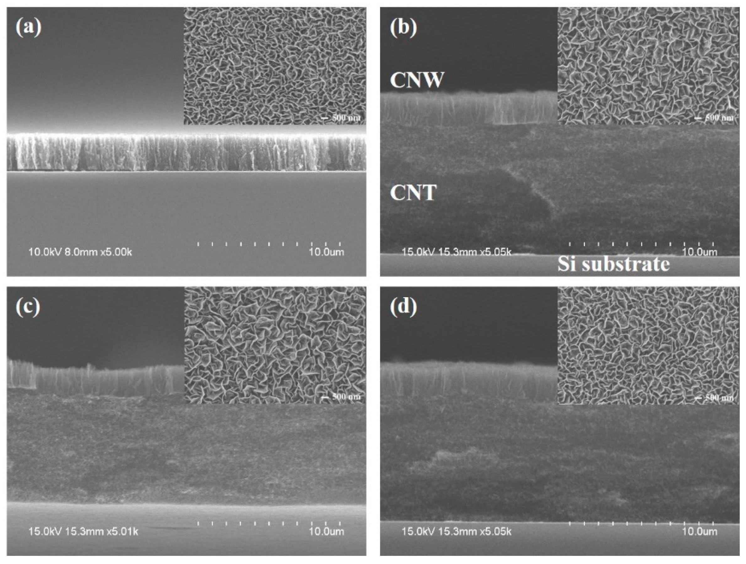
Figure 2 shows the image of FE-SEM of pristine CNW and MWCNT/CNW. The pristine CNW showed tight cross-sections with typical CNW morphology with various nano-porous surface (
Figure 2a). On the other hand, all samples where MWCNT was used as the buffer layer exhibited thick buffer layers compared to the pristine CNW (
Figure 2b–d). The thickness of the MWCNT-based buffer layer with 30, 50, 70 µL was 7.8, 8.3, and 8.7 µm, respectively. As the concentration increased, the buffer layer tended to become thicker. The height of CNW examined in all samples was 1.8~2.0 µm. In surface FE-SEM, only the arrangement of nanowalls was different with no-change in shape and density. These no-change of the CNW surface is different from the carbon nanowalls grown on different substrates [
8].
Figure 3 shows the Raman spectra results of all samples. In
Figure 3a, three peaks that can be commonly found in carbon materials were identified. Three common peaks are D peak (1350 cm
−1), G peak (1580 cm
−1), and 2D peak (2700 cm
−1). The D peak near 1350 cm
−1 can confirm the degree of defects due to the alignment of the carbon crystals. The high D peaks were observed in all samples, and these characteristics can be easily investigated in CNT and CNW. G peaks near 1580 cm
−1 are common in graphite-based carbon materials. The higher the intensity of the G peak, the better the graphitization and the better the carbon material. Then, the D peak occurred at 1620 cm
−1 was able to be examined only in CNW. This peak is mainly discovered at the edge of graphene. CNW is vertically grown with multiple graphene layer on a substrate, and the top of CNW may be opened to the edge of graphene. In addition, CNW has a large number of carbon branches, and the peak of D peak can be occurred because the end of this branch can have the shape of a graphene edge. On the other hand, in the case of CNT, single or multilayer graphene layers are curled and the edge of the graphene cannot be identified, so D peak does not appear. The 2D peak of 2700 cm
−1 appeared in all samples, and as the I
2D/I
G ratio of 0.5 or less was confirmed, it may imply that all samples had a multilayer graphene structure.
Figure 3b shows the I
D/I
G ratio of all samples. The I
D/I
G ratio numerically shows the carbon material defects, and the lower the ratio, the better the quality of the carbon material. All CNW specimens had a higher I
D/I
G ratio than CNT. With this phenomenon, the mechanism of growth of carbon nanowalls began with a defect by mismatch of carbon onions formed on the amorphous carbon buffer layer [
9]. When MWCNT is used as a buffer layer, carbon radicals by CVD can induce C-C bonds with MWCNTs, not substrates, thereby forming graphitic layers more than amorphous carbon. It may be a cause that can lead to improved electrical properties. In addition, carbon nanowalls usually change in structure and properties depending on the substrate [
10,
11,
12]. In our research, it is suggested that the structure of all specimens was unchanged because it was a synthesis reaction between the carbon-based substrate and carbon radical, not a reaction to the Si-substrate and the carbon radical, and it caused a non-variation of Raman spectra results.
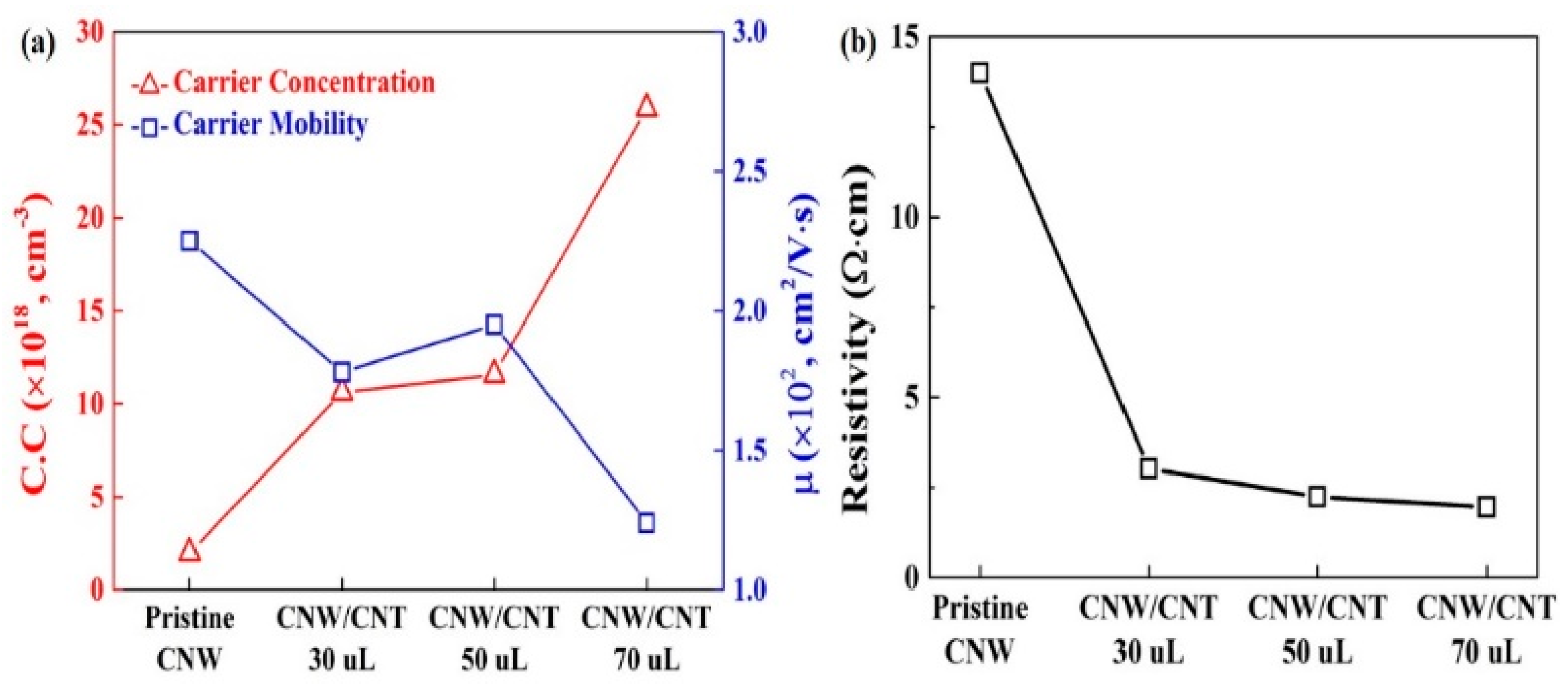
Figure 4 shows the electrical properties of carbon nanowalls grown on MWCNT-based buffer layers. In the Raman spectra, CNW grown on the MWCNT-based buffer layer was not significantly different from normal CNW. However, interesting results were found in the electrical properties results. First, in the case of carrier concentration, an improvement was observed with the increase of the CNT content forming the MWCNT-based buffer layer compared to the pristine CNW. The carbon buffer layer, which plays an important role in the general CNW nucleation and growth mechanism, is an amorphous carbon layer, so excellent electrical properties cannot be expected. While the MWCNT-based buffer layer has better electrical properties than the amorphous carbon layer, it is considered to contribute to the improvement of carrier concentration because it contains many carriers as a semiconductor impurity concept. Second, the carrier mobility was found to be inversely proportional to the carrier concentration. This phenomenon may be caused by alignment and defects in the carbon lattice. The MWCNT-based buffer layer underneath the CNW also has a high carbon lattice disorder similar to that of the CNW, which can significantly affect carrier mobility. The resistivity characteristic was analyzed to decrease with the increase of CNT content. This is because the carrier concentration is dominant in resistive properties, and the increase in the number of carriers by the CNT is expected to lead to a decrease in the resistivity. For this reason, samples containing 70 µL of CNTs showed the outstanding carrier concentration and resistivity.
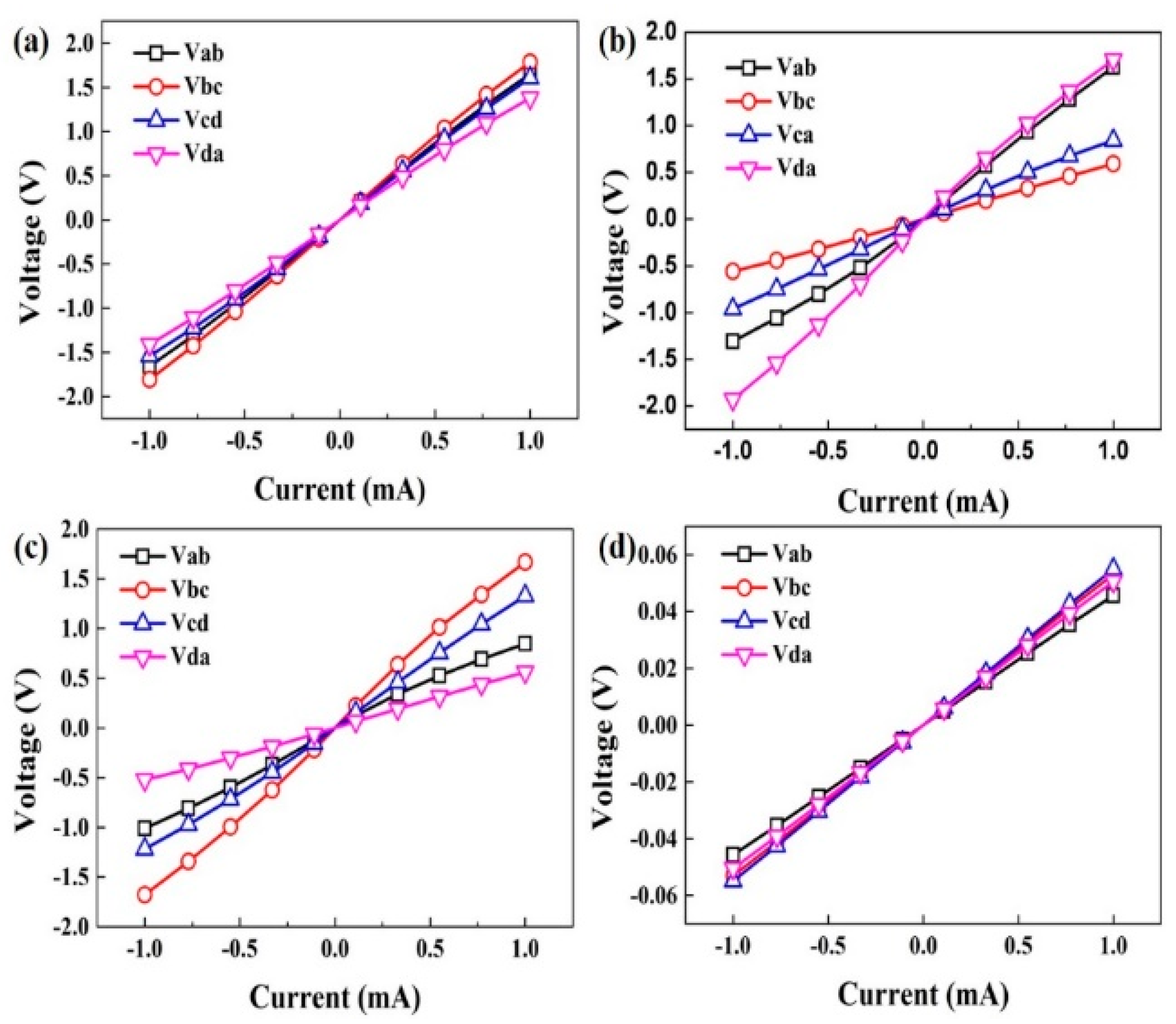
Figure 5 shows the I-V characteristics of pristine CNW, MWCNT (30 µL)/CNW, MWCNT (50 µL)/CNW and MWCNT (70 µL)/CNW samples. As shown in
Figure 1c, four probe tips were contacted at the edge of a sample having a size of 1 cm × 1 cm to apply a voltage of −1 mV to +1 mV. The slopes of the curves were different for all samples, but a linear I-V curve was observed. Since the slope of the curve represents the measured resistance value, it does not have much significance for the stability of the electrical characteristics. However, linearity is the most important factor because it implies that a constant current and resistance are maintained whenever the applied voltage changes. The V-I characteristics appear that all samples are electrically stable, which is due to ohmic contacts, not schottky contacts.
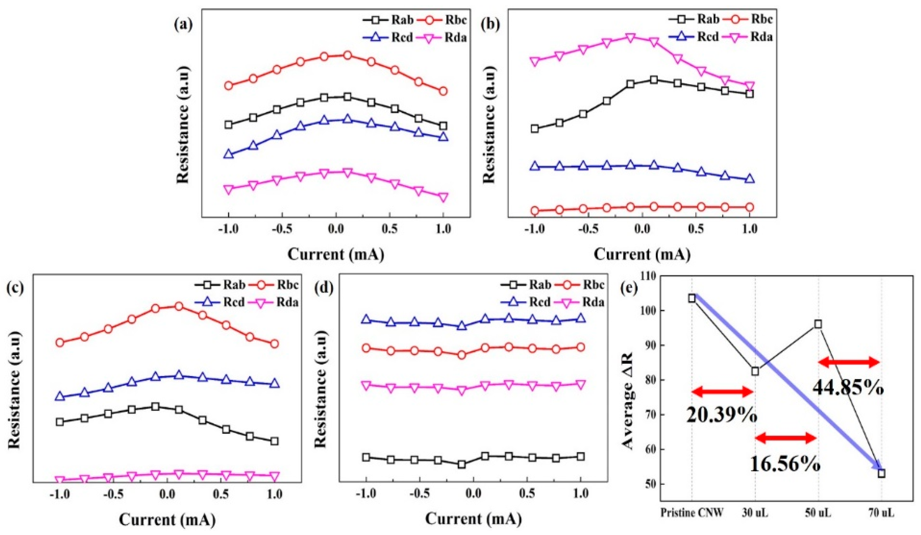
Figure 6 shows the change in resistance with the applied current as an I-R characteristic and average ΔR with percentage. An important factor of the I-R characteristics is linearity. This is because the resistance does not change even when the current changes, which means that it is electrically stable. In pristine CNW, parabolic curves were observed in all sections, indicating that there is a change in resistance due to current changes, suggesting this sample is not stable. In the CNW sample formed on the MWCNT-based buffer layer, the improved linearity occurred. As the CNT content was increased, the linearity was dramatically improved. As shown in
Figure 6d, the I-R characteristics with a CNT content of 70 µL show highly improved linearity. However, in
Figure 6b,c, partial nonlinearities have been identified. It is noted that these phenomena may be caused by structural changes in CNTs and CNWs, and defects caused by various factors.
In addition, stability test was conducted by obtaining the average ΔR at all points of each sample, and it means the better stability with lower ΔR. As expected, the pristine CNW showed the largest ΔR because the amorphous carbon was formed into the buffer layer, causing the charge transfer to be inconsistent. The sample with 30 µL of a MWCNT-based buffer layer showed a 20.39% decrease compared to pristine CNW. The samples using MWCNT with the highest concentration of 70 µL showed the lowest variation and the outstanding stability. It is noted that the sudden increase in the sample with 50 µL may be due to surface contamination during drying of the MWCNT after dropping MWCNT onto the Si substrate. Additionally, when measuring the hall measurement, such a phenomenon may occur because of scratches on the surface.
4. Conclusions
Carbon nanowalls show low electrical properties due to the amorphous buffer layer. In order to improve this portion, the MWCNT was used as a buffer layer, and the structural and electrical properties were studied. The structural characteristics by Raman spectra were not significantly different from those of general CNWs. This is because the Raman spectra only analyzes the edge part of a thin film surface, not bulk analysis, suggesting that the CNW has been successfully grown on MWCNT-based buffer layers. The dramatic changes were identified in the electrical characterization. As the CNT content increased, the carrier concentration was improved and the resistivity was dramatically decreased. In the I-V characteristics, all samples showed linearity, indicating that they were electrically stable, and a successful ohmic contact could be expected. CNW samples with MWCNT-based buffer layers showed improvement of I-R linearity compared with pristine CNW, and samples containing 70 µL of CNTs showed perfect straight lines and perfect stable properties. CNW is a carbon material which has characteristics that differ greatly by pre-treatment, unlike graphene and CNT. In this study, electrical characteristics of CNWs were improved by pre-treatment of MWCNT-based buffer layers. As such, the electrical characteristic conversion method, according to the pre-treatment, is expected to have a high influence on various devices such as biosensors and gas sensors, which will be used in the future.
