Improvement of Electrical Performance in Heterostructure Junctionless TFET Based on Dual Material Gate


Abstract
1. Introduction
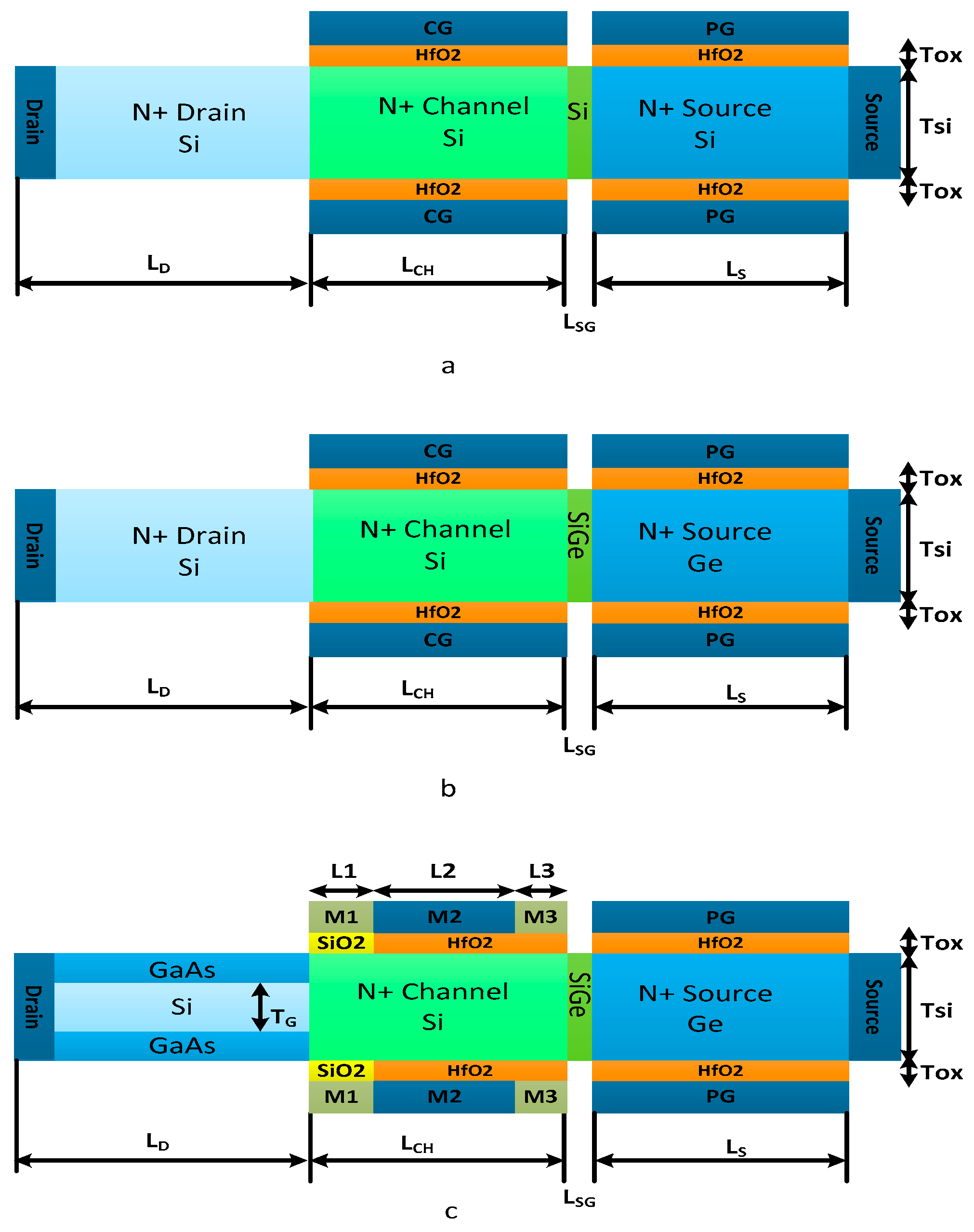
2. Methods
3. Results and Discussion
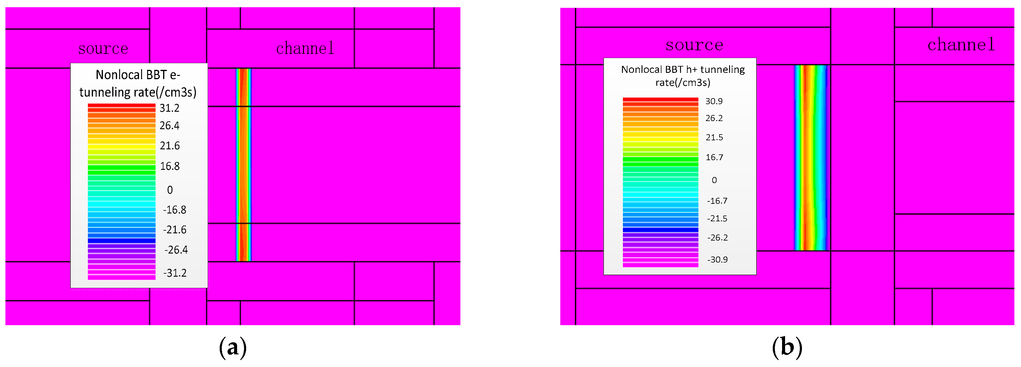
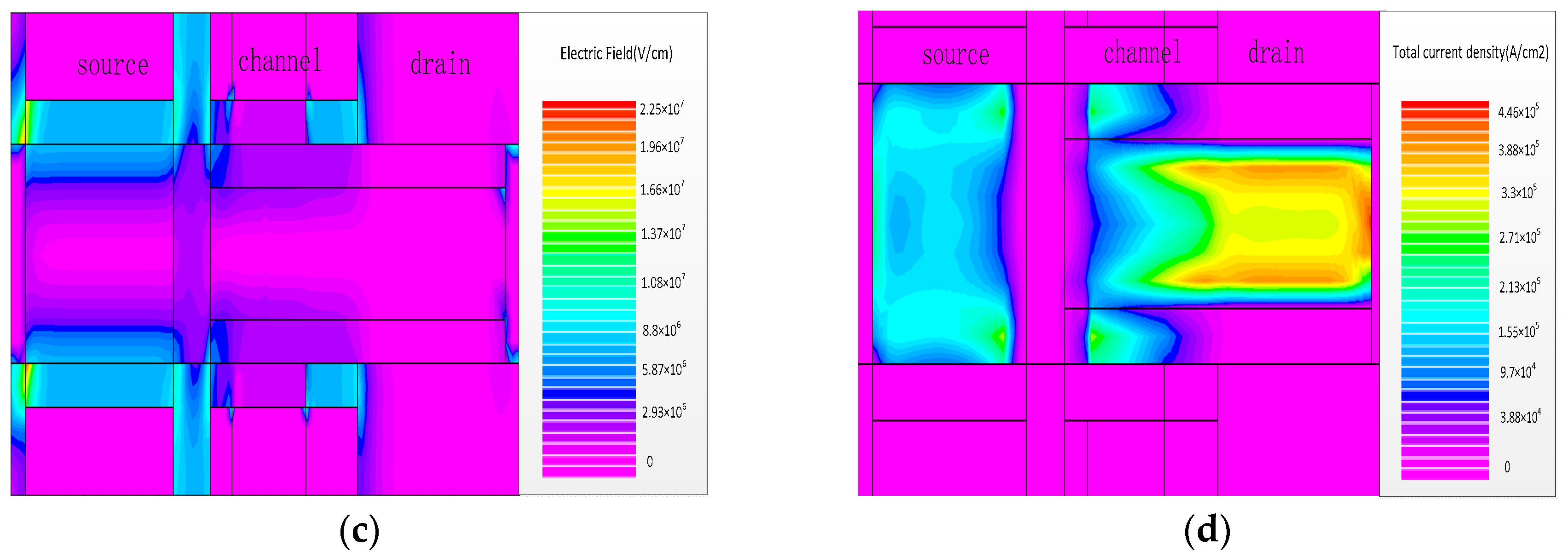
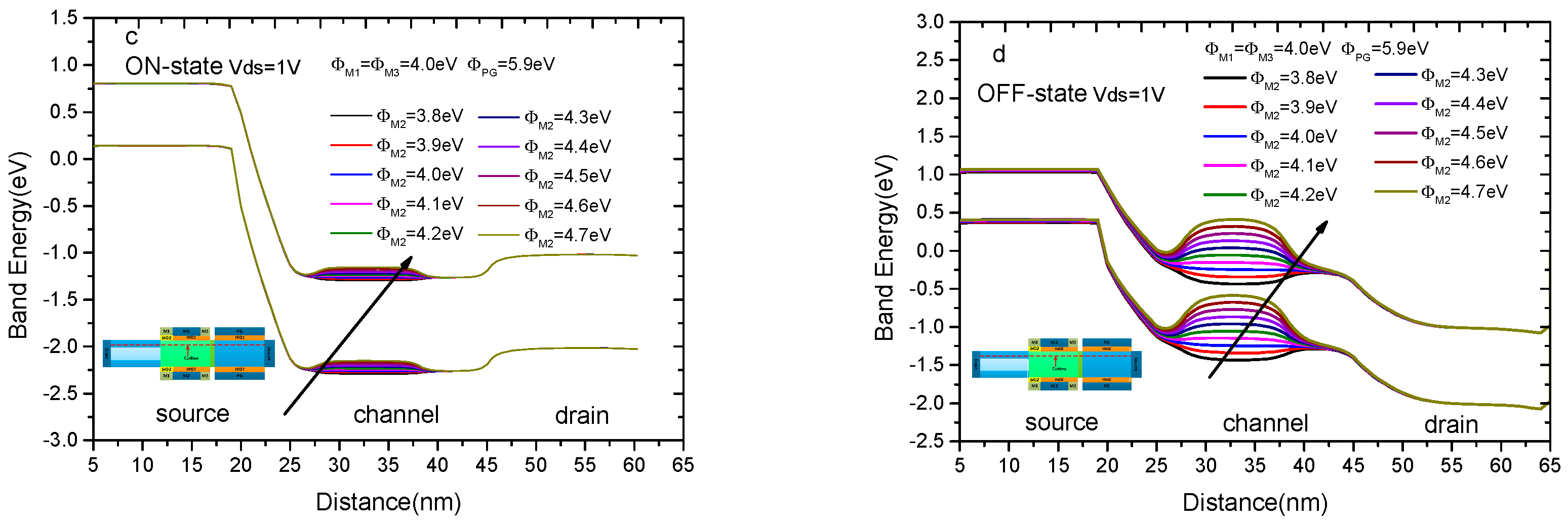
3.1. The Operating Mechanism of DMMG-HJLTFET
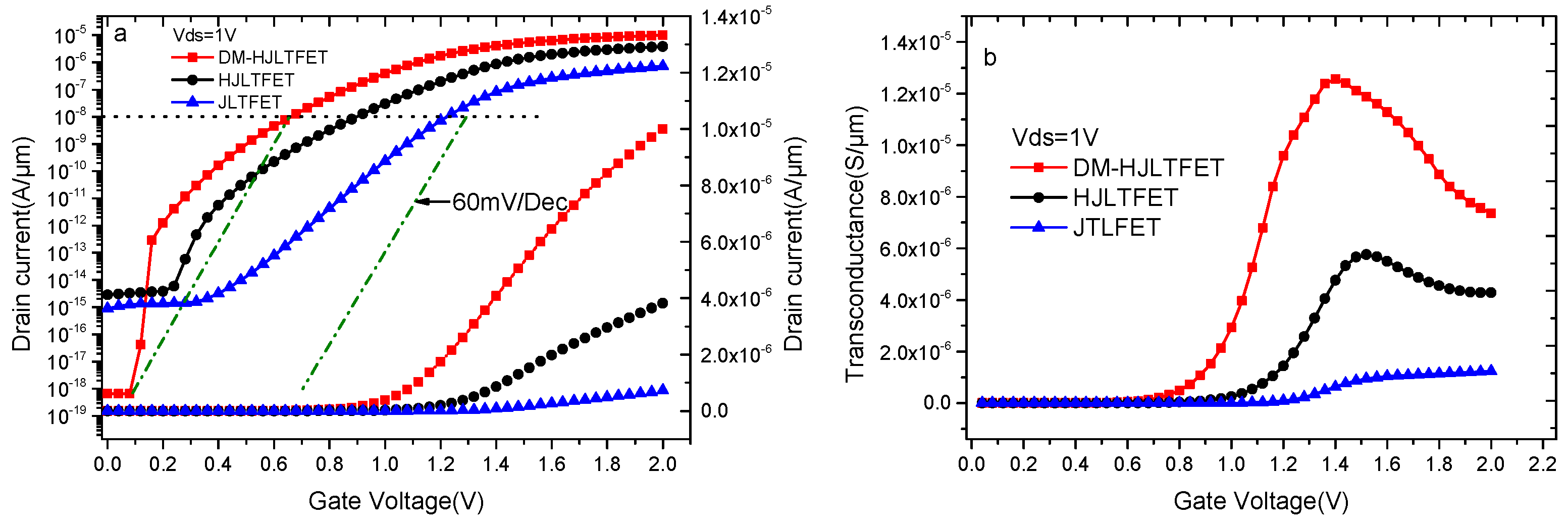
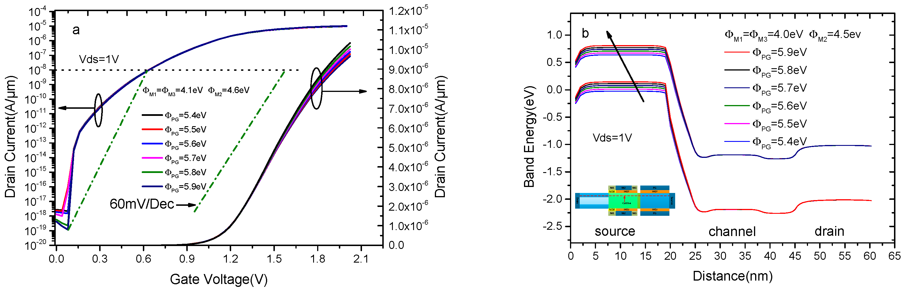
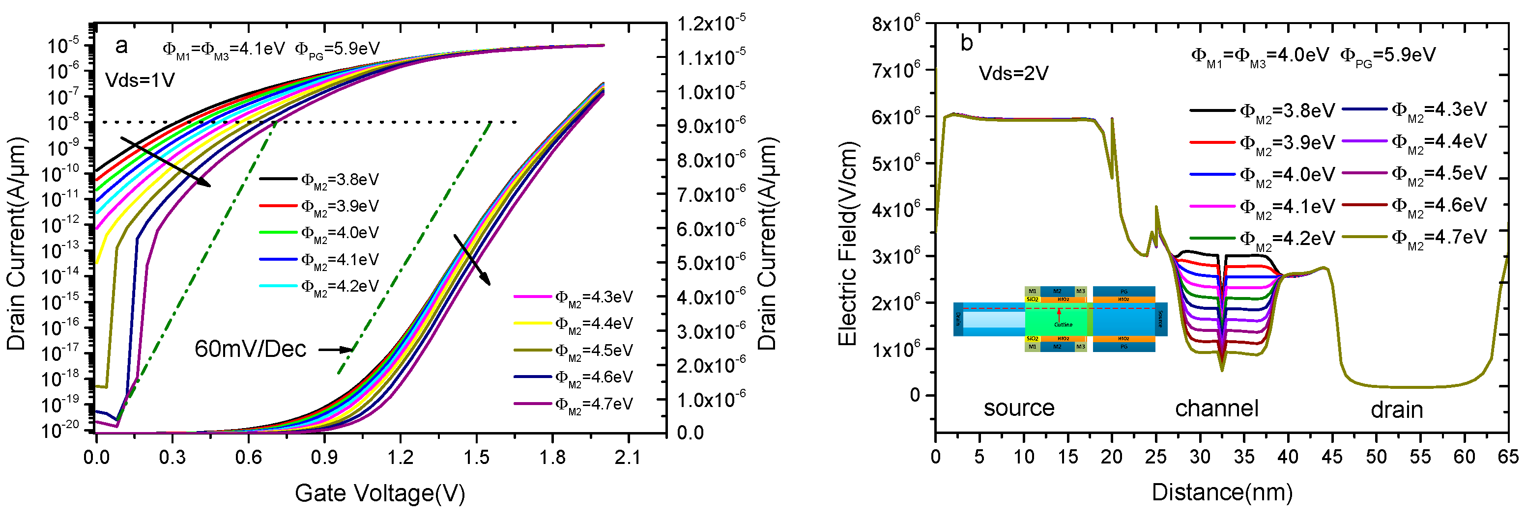
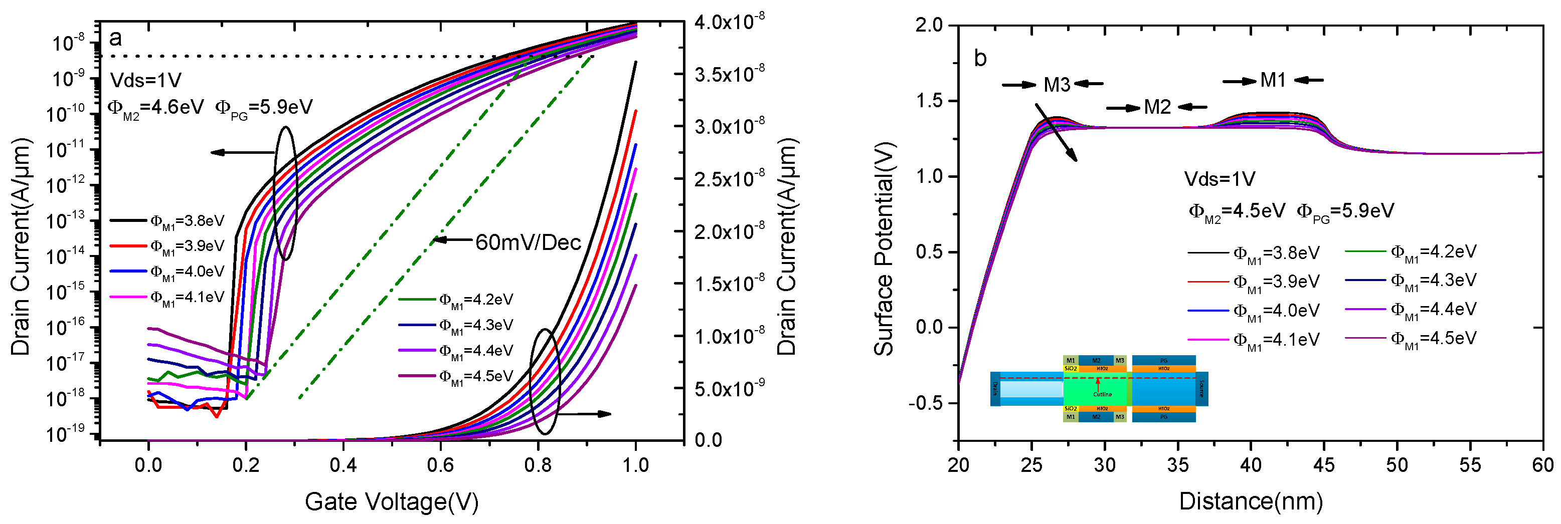
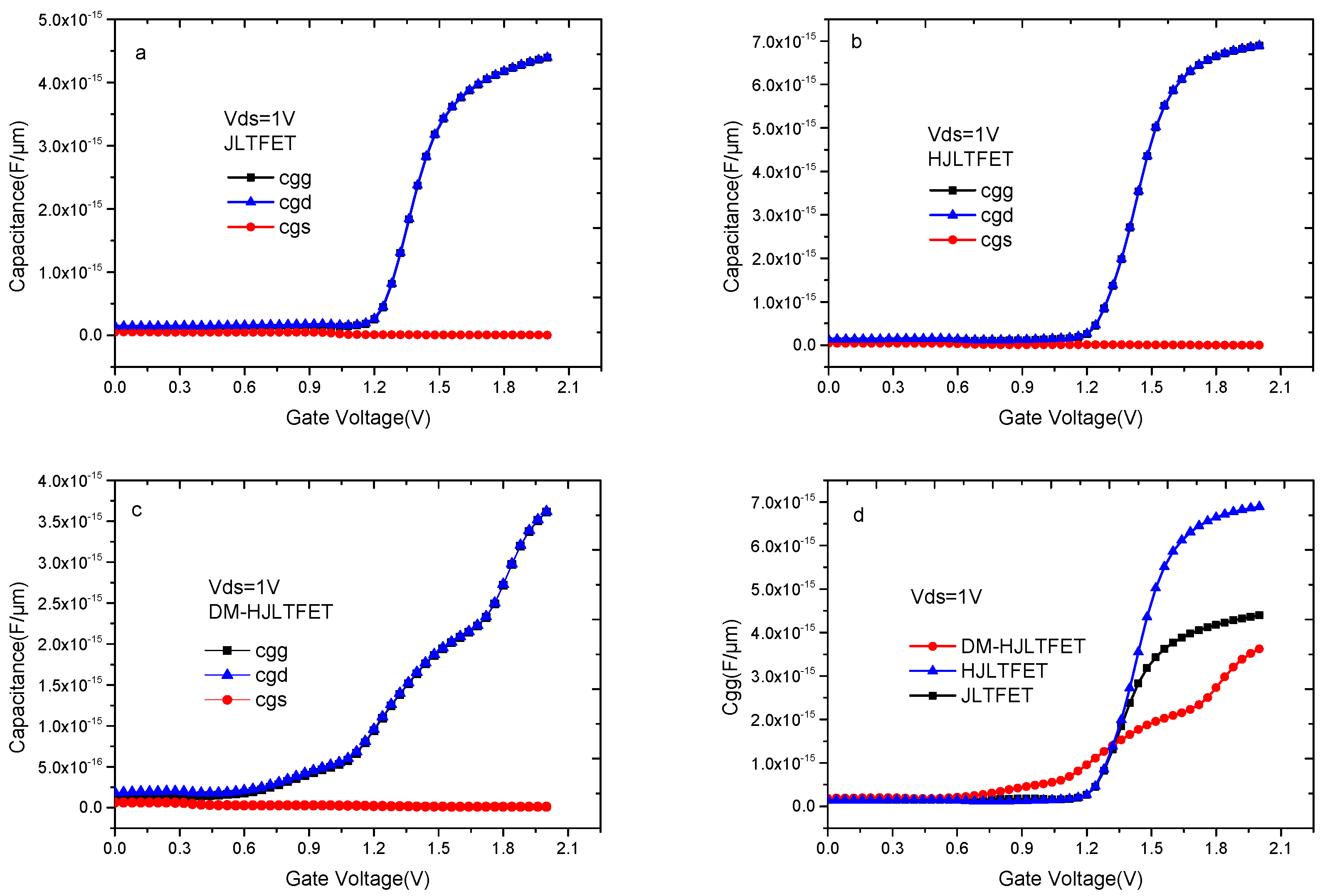
3.2. The Input Characteristics
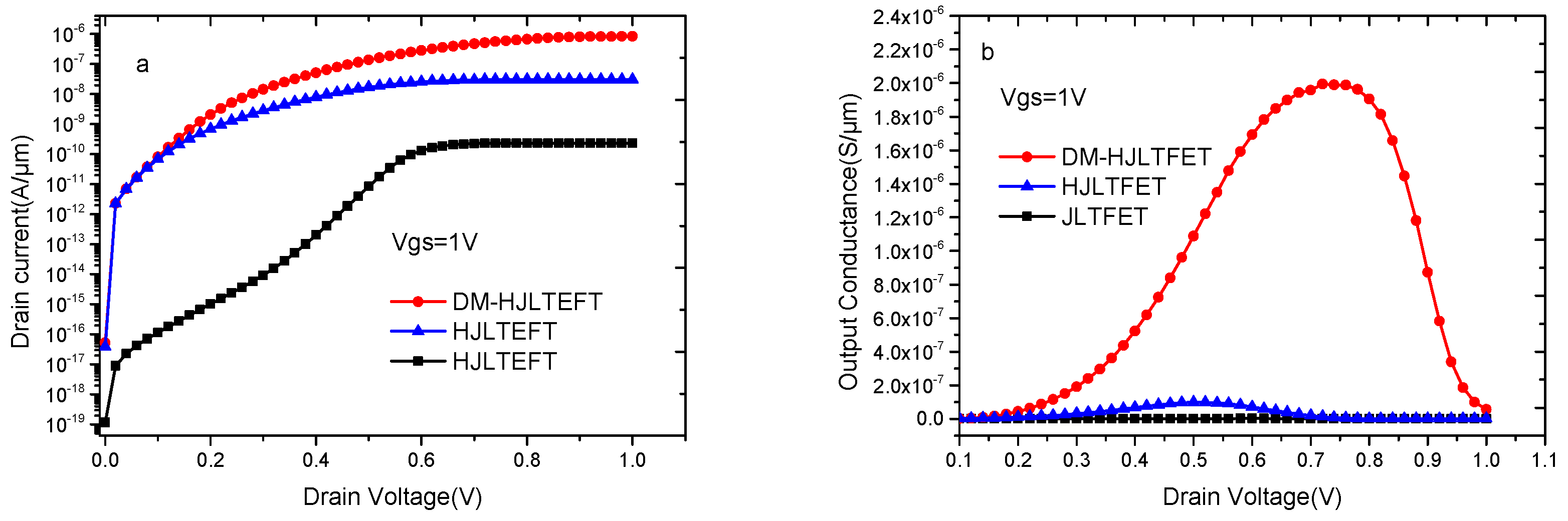
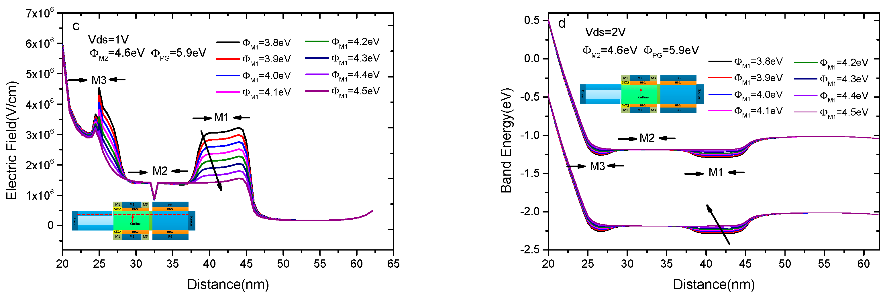
3.3. The Output Characteristics
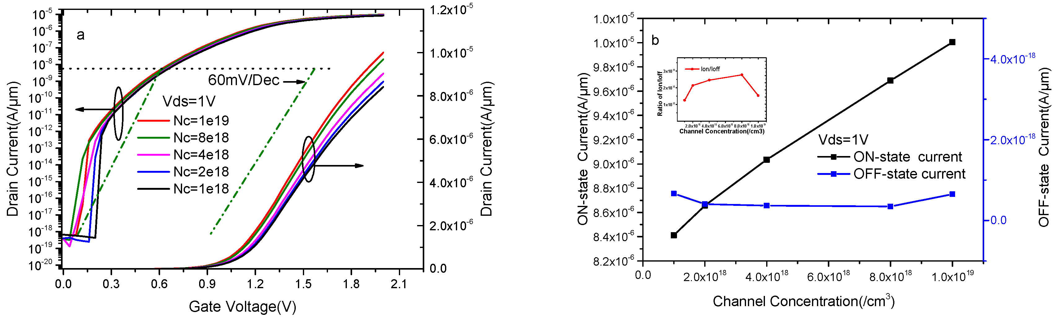
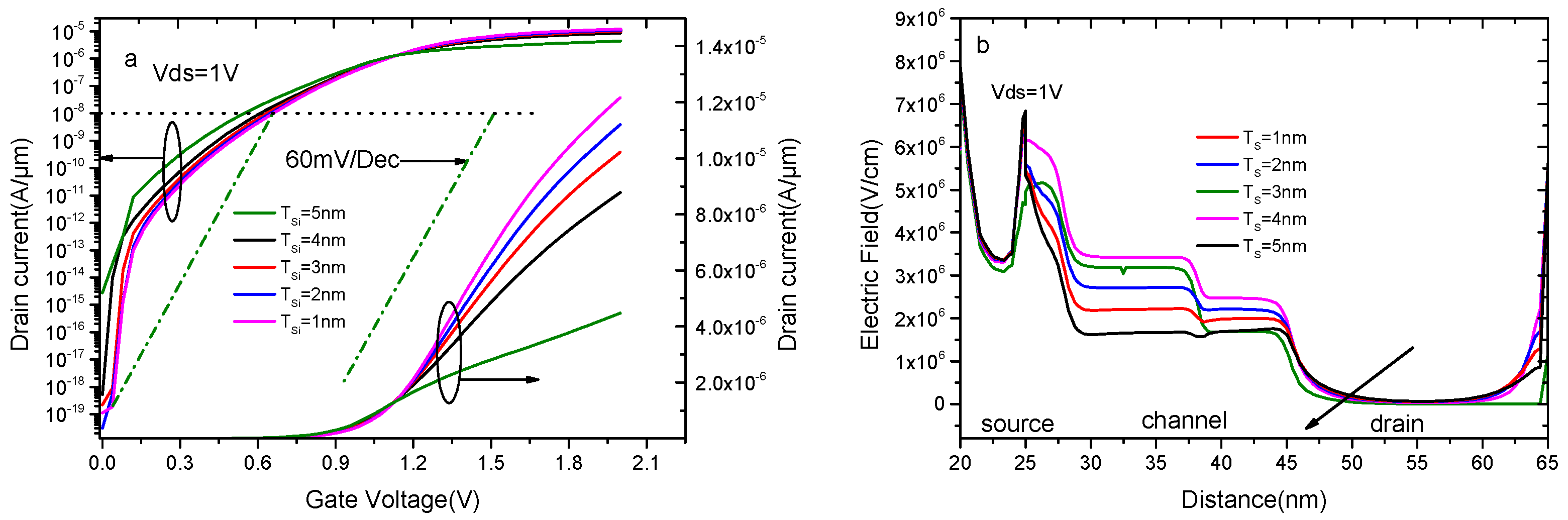
3.4. Effect of Device Sizes on the Transfer Characteristics
3.5. Performance Comparison in Terms of Analog/RF Figure of Merits
4. Conclusions
Author Contributions
Funding
Conflicts of Interest
References
- Choi, W.Y.; Park, B.-G.; Lee, J.D.; Liu, T.-J.K. Tunneling field-effect transistors (TFETs) with subthreshold swing (SS) less than 60 mV/dec. IEEE Electron Device Lett. 2007, 28, 743–745. [Google Scholar] [CrossRef]
- Anghel, C.; Gupta, A.; Amara, A.; Vladimirescu, A. 30-nm Tunnel FET with Improved Performance and Reduced Ambipolar Current. IEEE Trans. Electron Devices 2011, 58, 1649–1654. [Google Scholar] [CrossRef]
- Jang Hyun, K.; Sangwan, K.; Byung-Gook, P. Double-Gate TFET with Vertical Channel Sandwiched by Lightly Doped Si. IEEE Trans. Electron Devices 2019, 66, 1656–1661. [Google Scholar]
- Mohd, R.U.S.; Sajad, A.L. Drain-Engineered TFET with Fully Suppressed Ambipolarity for High-Frequency Application. IEEE Trans. Electron Devices 2019, 66, 1628–1634. [Google Scholar]
- Verhulst, A.S.; Vandenberghe, W.G.; Maex, K.; De Gendt, S.; Heyns, M.M.; Groeseneken, G. Complementary silicon-based heterostructure tunnel-FETs with high tunnel rates. IEEE Electron Device Letter 2008, 29, 1398–1401. [Google Scholar] [CrossRef]
- Ahn, D.H.; Yoon, S.H.; Kato, K.; Fukui, T.; Takenaka, M.; Takagi, S. Effects of ZrO2/Al2O3 Gate-Stack on the Performance of Planar-Type InGaAs TFET. IEEE Trans. Electron Devices 2019, 66, 1862–1867. [Google Scholar] [CrossRef]
- Avci, U.E.; Young, I.A. Heterojunction TFET scaling and resonant-TFET for steep subthreshold slope at sub-9nm gate-length. In Proceedings of the IEEE IEDM, Washington, DC, USA, 9–11 December 2013; pp. 4.3.1–4.3.4. [Google Scholar]
- Zhaonian, Y. Tunnel Field-Effect Transistor with an L-Shaped Gate. IEEE Trans. Electron Devices 2016, 37, 839–842. [Google Scholar]
- Kim, S.W.; Kim, J.H.; Liu, T.-J.K.; Choi, W.Y.; Park, B.G. Demonstration of L-Shaped Tunnel Field-Effect Transistors. IEEE Trans. Electron Devices 2016, 63, 1774–1778. [Google Scholar] [CrossRef]
- Najam, F.; Yu, Y.S. Impact of Quantum Confinement on Band-to-Band Tunneling of Line-Tunneling Type L-Shaped Tunnel Field-Effect Transistor. IEEE Trans. Electron Devices 2019, 66, 2010–2016. [Google Scholar] [CrossRef]
- Kim, J.H.; Kim, S.; Park, B.-G. Symmetric U-Shaped Gate Tunnel Field-Effect Transistor. IEEE Trans. Electron Devices 2017, 64, 1343–1349. [Google Scholar]
- Wang, W.; Wang, P.F.; Zhang, C.M.; Lin, X.; Liu, X.Y.; Sun, Q.Q.; Zhou, P.; Zhang, D.W. Design of U-Shape Channel Tunnel FETs with SiGe Source Regions. IEEE Trans. Electron Devices 2014, 61, 193–197. [Google Scholar] [CrossRef]
- Nam, H.; Cho, M.H.; Shin, C. Symmetric tunnel field-effect transistor (S-TFET). Curr. Appl. Phys. 2015, 15, 71–77. [Google Scholar] [CrossRef]
- Lee, H.; Park, S.; Lee, Y.; Nam, H.; Shin, C. Random variation analysis and variation-aware design of symmetric tunnel field-effect transistor. IEEE Trans. Electron Devices 2015, 62, 1778–1783. [Google Scholar]
- Jiang, Z.; Zhuang, Y.; Li, C.; Wang, P. Dual Sources U-shape Gate Tunnel FETs with High On-current and Steep SS. In Proceedings of the 2016 16th International Workshop on Junction Technology (IWJT), Shanghai, China, 9–10 May 2015; pp. 25–27. [Google Scholar]
- Sola, W.; Sangsig, K. Covered Source–Channel Tunnel Field-Effect Transistors with Trench Gate Structures. IEEE Trans. Nanotechnol. 2018, 18, 114–118. [Google Scholar]
- Li, W.; Liu, H.; Wang, S.; Chen, S.; Yang, Z. Design of High Performance Si/SiGe Heterojunction Tunneling FETs with a T-Shaped Gate. Nanoscale Res. Lett. 2017, 12, 198. [Google Scholar] [CrossRef] [PubMed]
- Áron, S.; Steven, J.K.; Mathieu, L. Ab-Initio Simulation of van der Waals MoTe2–SnS2. Heterotunneling FETs for Low-Power Electronics. IEEE Electron Device Lett. 2015, 36, 514–516. [Google Scholar]
- Cao, J.; Logoteta, D.; Özkaya, S.; Biel, B.; Cresti, A.; Pala, M.G.; Esseni, D. Operation and Design of van der Waals Tunnel Transistors: A 3-D Quantum Transport Study. IEEE Trans. Electron Devices 2016, 63, 4388–4394. [Google Scholar] [CrossRef]
- Singh, D.; Pandey, S.; Nigam, K.; Sharma, D.; Yadav, D.S.; Kondekar, P. A Charge-Plasma-Based Dielectric-Modulated Junctionless TFET for Biosensor Label-Free Detection. IEEE Trans. Electron Devices 2018, 64, 271–278. [Google Scholar] [CrossRef]
- Aslam, M.; Sharma, D.; Yadav, S.; Soni, D.; Sharma, N.; Gedam, A. A comparative investigation of low work-function metal implantation in the oxide region for improving electrostatic characteristics of charge plasma TFET. Micro Nano Lett. 2019, 14, 123–128. [Google Scholar] [CrossRef]
- Haiwu, X.; Hongxia, L.; Shupeng, C.; Tao, H.; Shulong, W. Design and Investigation of a Dual Material Gate Arsenic Alloy Heterostructure Junctionless TFET with a Lightly Doped Source. Appl. Sci. 2019, 9, 4104. [Google Scholar]
- Tao, H.; Hongxia, L.; Shupeng, C.; Shulong, W.; Wei, L. Design and Investigation of the High Performance Doping-Less TFET with Ge/Si0.6Ge0.4/Si Heterojunction. Micromachines 2019, 10, 424. [Google Scholar]
- Aghandeh, H.; Ziabari, S.A.S. Gate engineered heterostructure junctionless TFET with Gaussian doping profile for ambipolar suppression and electrical performance improvement. Superlattices Microstruct. 2017, 111, 103–134. [Google Scholar] [CrossRef]
- Rouzbeh, M.I.A.; Seyed, A.S.Z. Improved performance of nanoscale junctionless tunnel field-effect transistor based on gate engineering approach. Appl. Phys. A Mater. Sci. Process. 2016, 122, 988. [Google Scholar]
- Rahimian, M.; Fathipour, M. Improvement of electrical performance in junctionless nanowire TFET using hetero-gate-dielectric. Mater. Sci. Semicond. Process. 2017, 63, 142–152. [Google Scholar] [CrossRef]
- Anju; Tirkey, S.; Nigam, K.; Pandey, S.; Sharma, D.; Kondekar, P. Investigation of gate material engineering in junctionless TFET to overcome the trade-off between ambipolarity and RF/linearity metrics. Superlattices Microstruct. 2017, 109, 307–315. [Google Scholar] [CrossRef]
- Basak, S.; Asthana, P.K.; Goswami, Y. Leakage current reduction in junctionless tunnel FET using a lightly. Doped source. Appl. Phys. 2015, 118, 1527–1533. [Google Scholar] [CrossRef]
- Bal, P.; Akram, M.W.; Mondal, P.; Ghosh, B. Performance estimation of sub-30 nm junctionless tunnel FET (JLTFET). J. Comput. Electron. 2013, 12, 782–789. [Google Scholar] [CrossRef]
- Lee, J.C.; Ahn, T.J.; Yu, Y.S. Si/Ge Hetero Tunnel Field-Effect Transistor with Junctionless Channel Based on Nanowire. J. Nanosci. Nanotechnol. 2019, 19, 6750–6754. [Google Scholar] [CrossRef]
- Leung, G.; Chui, C.O. Variability impact of random dopant fluctuation on nanoscale junctionless FinFETs. IEEE Electron Device Lett. 2012, 33, 767–769. [Google Scholar] [CrossRef]
- Wang, H.; Jiang, L.L.; Wang, N.; Yu, H.Y.; Lin, X.P. A Charge Storage Based Enhancement Mode AlGaN/GaN High Electron Mobility Transistor. Mater. Sci. Forum 2018, 913, 870–875. [Google Scholar] [CrossRef]
- Pezzimenti, F. Modeling of the steady state and switching characteristics of a normally-off 4H-SiC trench bipolar-mode FET. IEEE Trans. Electron Devices 2013, 60, 1404–1411. [Google Scholar] [CrossRef]
- Anvarifard, M.K.; Orouji, A.A. Proper Electrostatic Modulation of Electric Field in a Reliable Nano-SOI with a Developed Channel. IEEE Trans. Electron Devices 2018, 65, 1653–1657. [Google Scholar] [CrossRef]
- Francesco, G.D.C.; Fortunato, P.; Salvatore, B.; Roberta, N. Numerical simulations of a 4H-SiC BMFET power transistor with normally-off characteristics. Mater. Sci. Forum 2011, 679–680, 621–624. [Google Scholar]
- Sarkar, A.; Sarkar, C.K. RF and analogue performance investigation of DG tunnel FET. Electron. Lett. 2010, 1, 210–217. [Google Scholar] [CrossRef]
- Seema, N.; Sudakar, S.C. Investigation of RF and linearity performance of electrode work-function engineered HDB vertical TFET. Micro Nano Lett. 2019, 14, 17–21. [Google Scholar]
- Chen, S.; Liu, H.; Wang, S.; Li, W.; Wang, X.; Zhao, L. Analog/RF Performance of T-Shape Gate Dual-Source Tunnel Field-Effect Transistor. Nanoscale Res. Lett. 2018, 13, 321. [Google Scholar] [CrossRef]


| Parameter Name | JLTFET | HJLTFET | DMMG-HJLTFET |
|---|---|---|---|
| Length of source (LS/nm) | 20 | 20 | 20 |
| Length of channel (LCH/nm) | 20 | 20 | 20 |
| Length of drain (LD/nm) | 20 | 20 | 20 |
| Length of gap (LSG/nm) | 5 | 5 | 5 |
| Thickness of SiO2 and HfO2(TOX/nm) | 2 | 2 | 2 |
| Thickness of the silicon body (Tsi/nm) | 5 | 5 | 5 |
| Thickness of the Si (TS/nm) in sandwich stack | 3 | 3 | 3 |
| Length of auxiliary gate(L1/nm) | 7 | ||
| Length of control gate(L2/nm) | 10 | ||
| Length of tunnel gate(L3/nm) | 3 | ||
| Work function of polarity gate(ΦPG/eV) | 5.9 | 5.9 | 5.9 |
| Work function of control gate(ΦCG/eV) | 4.6 | 4.6 | 4.6 |
| Work function of auxiliary gate(ΦM1/eV) | 4.1 | ||
| Work function of tunnel gate(ΦM3/eV) | 4.1 | ||
| N-type doping concentration (NC/cm−3) | 1 × 10¹⁹ | 1 × 10¹⁹ | 1 × 10¹⁹ |
| Ion (A/μm) | Ioff (A/μm) | Ion/Ioff | gm (S/μm) | SS (mV/Dec) | |
|---|---|---|---|---|---|
| JLTFET | 7.21 × 10⁻⁷ | 1.36 × 10⁻¹⁵ | 5.3 × 10⁸ | 1.22 × 10⁻⁶ | 122 |
| HJLTFET | 3.82 × 10⁻⁶ | 2.84 × 10⁻¹⁵ | 1.34 × 10⁹ | 5.76 × 10⁻⁶ | 88.2 |
| DMMG-HJLTFET | 1.01 × 10⁻⁵ | 6.5 × 10⁻¹⁹ | 1.56 × 10¹³ | 1.26 × 10⁻⁵ | 52 |
© 2019 by the authors. Licensee MDPI, Basel, Switzerland. This article is an open access article distributed under the terms and conditions of the Creative Commons Attribution (CC BY) license (http://creativecommons.org/licenses/by/4.0/).
Share and Cite
Xie, H.; Liu, H.; Wang, S.; Chen, S.; Han, T.; Li, W. Improvement of Electrical Performance in Heterostructure Junctionless TFET Based on Dual Material Gate. Appl. Sci. 2020, 10, 126. https://doi.org/10.3390/app10010126
Xie H, Liu H, Wang S, Chen S, Han T, Li W. Improvement of Electrical Performance in Heterostructure Junctionless TFET Based on Dual Material Gate. Applied Sciences. 2020; 10(1):126. https://doi.org/10.3390/app10010126
Chicago/Turabian StyleXie, Haiwu, Hongxia Liu, Shulong Wang, Shupeng Chen, Tao Han, and Wei Li. 2020. "Improvement of Electrical Performance in Heterostructure Junctionless TFET Based on Dual Material Gate" Applied Sciences 10, no. 1: 126. https://doi.org/10.3390/app10010126
APA StyleXie, H., Liu, H., Wang, S., Chen, S., Han, T., & Li, W. (2020). Improvement of Electrical Performance in Heterostructure Junctionless TFET Based on Dual Material Gate. Applied Sciences, 10(1), 126. https://doi.org/10.3390/app10010126