Abstract
Advancements in software engineering have enabled the robotics industry to transition from the use of giant industrial robots to more friendly humanoid robots. Soft robotics is one of the key elements needed to advance the transition process by providing a safer way for robots to interact with the environment. Electroactive polymers (EAPs) are one of the best candidate materials for the next generation of soft robotic actuators and artificial muscles. Lightweight dielectric elastomer actuators (DEAs) provide optimal properties such as high elasticity, rapid response rates, mechanical robustness and compliance. However, for DEAs to become widely used as artificial muscles or soft actuators, there are current limitations, such as high actuation voltage requirements, control of actuation direction, and scaling, that need to be addressed. The authors’ approach to overcome the drawbacks of conventional DEAs is inspired by the natural skeletal muscles. Instead of fabricating a large DEA device, smaller sub-units can be fabricated and bundled together to form larger actuators, similar to the way myofibrils form myocytes in skeletal muscles. The current study presents a novel fabrication approach, utilizing soft lithography and other microfabrication techniques, to allow fabrication of multilayer stacked DEA structures, composed of hundreds of micro-sized DEA units.
1. Introduction
Soft robotics is a new and emerging field that aims to develop robots with soft structures to provide a safer and more flexible working environment where robots can interact with humans and other objects, with abated safety concerns, yet still be able carry out significant tasks that conventional rigid robots cannot [1]. There have been numerous studies in recent years to develop different types of soft structures, such as inflatable actuators, electromechanical actuators, flexible skin sensors, stretchable tactile sensors, and energy harvesters for soft robotics [1,2,3]. A promising candidate class of materials that could be suitable for soft robotics as well as other application areas is electroactive polymers (EAPs).
The concept of EAPs, materials that physically respond to external electrical stimuli by changing their shape and volume, was first realized in the late 19th century when Röntgen experimented with rubber bands [4]. With advancements in synthetic polymers, EAPs started to reemerge in the 1990s [5]. However, it was not until 2000, when Pelrine et al. reported [6] that approximately 215% actuation could be achieved with acrylic elastomers, that EAPs came into the spotlight for researchers interested in soft robotics. EAPs are made of flexible polymers, so they are inherently flexible, light, and, most of the time, stretchable. These attributes give the EAPs a significant advantage over traditional, rigid, metal actuators in applications where tolerance to elastic deformation is required and weight management is crucial.
Among the many different types of electroactive polymers, dielectric elastomer actuators (DEAs) are one of the most promising types. DEAs can provide high actuation speed and relatively high actuation forces while maintaining a flexible and stretchable actuator body. A dielectric elastomer actuator consists of three main parts: a dielectric membrane and two conductive parallel plates, one on each side of the dielectric material, as shown in Figure 1. When a voltage is applied, the conductive layers are charged with opposite charges, which creates a Coulombic attraction force. The force compresses the actuator in a perpendicular direction to the parallel electrodes. The elastomeric dielectric material between the conductive layers then expands in the lateral direction to conserve volume.
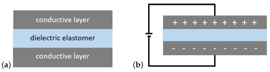
Figure 1.
Schematics show a cross-sectional view of a DEA in (a) its relaxed state and (b) actuated state when the voltage is applied. The black parts represent the conductive parallel layers and the grey part represents the dielectric elastomer.
2. Background
DEAs are suitable actuators for many applications, however a few limitations still need to be addressed. The most significant is the high voltage requirement for actuation, which is not practical for most applications [7,8,9]. There have also been different approaches taken to amplify the actuation ratio through mechanical improvements that can allow the DEAs to actuate more than 100% [4]. One of these approaches is to introduce prestrain to the dielectric membrane during fabrication. Although prestrain has been proven to increase the actuation ratio, it is not applicable in all cases. For example, if the DEAs are fabricated at smaller scales (i.e., the sub-millimeter scale), it is not practical to introduce prestrain mechanically [10]. Furthermore, prestraining may have a negative impact on the lifetime of DEAs [11].
In a DEA actuator, the magnitude of the force exerted on the dielectric membrane is directly related to the square of the applied voltage and inversely related to the square of the distance between the conductive parallel layers, which is equal to the thickness of the dielectric membrane. In ideal conditions, the ratio of total deformation in thickness of the dielectric layer to its original thickness can be calculated using
where U is the applied voltage, is the thickness of the dielectric layer (or the distance between the conductive layers), Y is Young’s modulus of the dielectric material, and are permittivity of free space and relative permittivity of the dielectric material respectively, and is the change in thickness of the dielectric layer.
Empirically, Equation (1) shows that, by reducing the separation distance of the conductive layer and thus the dielectric elastomer thickness, it is possible to reduce the input voltage of a DEA to obtain the same actuation ratio (). There have been studies focusing on miniaturization of DEAs using different approaches [10,12,13,14,15,16]. Dubois et al. introduced a fabrication method for a membrane type DEA and reported an out-of-plane displacement of 13%. Gerratt et al. introduced a fabrication method for a miniaturized cantilever type bidirectional DEA on silicon wafer using deep reactive ion etch for patterning [13]. They have reported significant bending displacement at voltage lower than 1 kV. In 2015, Poulin et al. printed a DEA with a 3 m dielectric membrane and reported 7.5% strain at 245 V [14]. In 2017, McCoul et al. improved the method to allow inkjet 3D printing of UV curable DEAs [16]. Xiaobin et al. introduced prestretch for micro-fabricated DEAs to increase the actuation ratio and reported about 4% strain at 100 V [17]. These studies provide unique contributions for miniaturization of DEAs and reducing the operating voltage of DEAs to sub-kV range. However, the fabricated DEAs using these methods rely on rigid substrates to work, allow fabrication of only single layer or trilayer actuators, provide small displacements in the micrometer range, output small forces, and cannot be scaled up to fabricate larger actuators.
In order to compensate for the loss in actuation distance, many layers of actuators can be stacked together to form a longer actuator structure. If all the stacked layers are connected in parallel, the input voltage required for actuation should be equivalent to the input voltage of a single DEA. Forming a long stacked structure also provides more physical space for interconnection of DEAs to other objects or materials. Kovacs et al. demonstrated the feasibility of fabricating stacked dielectric elastomer actuators with more than 200 dielectric elastomer layers [8]. Actuation ratios from 10 to 46% were achieved at different voltages up to 4.1 kV [8]. Recently, Duduta et al. introduced a microfabrication approach to fabricate multilayer DEAs on silicon wafer incorporating single walled carbon nanotube (SWCNT) electrodes [15]. They achieved a multilayer (12 layers) configuration by manually fabricating each subsequent layer on top of the previously fabricated layer. The reported energy density is comparable to other multilayer DEAs, but the resulting actuation is a bending motion. In order to obtain a significant linear actuation, the number of layers would have to be increased. The method could provide ultra-thin dielectric layers, however, it requires a meticulous alignment step for each layer which could add up to a significant amount of time as the number of layers increase.
In this study, novel soft lithoghraphy techniques, based on previous studies [18,19], are introduced to allow for fabrication of biomimetic stacked linear actuator systems at a small scale. The resulting structures have reduced the actuation voltages, increased actuation ratios, allowed for fabrication of free standing DEAs, and provided a feasible fabrication method to scale up the size of the actuators as needed for different applications.
3. Methods
3.1. Materials
One of the most commonly studied materials for fabricating DEAs is the commercially available 3M™ VHB™ tape (3M, Maplewood, MN, USA) [5,20,21,22,23]. VHB tape is a good candidate for DEAs in terms of cost, accessibility, and ease of fabrication. Large actuation distances (>100%) can be obtained with DEAs made of prestreched VHB tape as the dielectric layers coated with carbon based electrodes [5,21]. However, since the thickness of the VHB layer is usually predefined and large [24], the operating voltage is usually in the 3–5 kV range for these actuators. Furthermore, since VHB tape shows viscoelastic behavior under stress, its response time is limited and the actuation cannot be reversed as quickly as some other polymers with less pronounced viscoelastic behavior, such as polysiloxanes (silicones) or polyurethanes [7,24,25].
One of the most common silicone materials is poly(dimethyl siloxane) (PDMS). PDMS is a widely used polymer, especially for biomedical and microfluidic applications due its biocompatibility and ease of fabrication [26,27,28]. PDMS is a siloxane based viscoelastic polymer, but can be solidified with a curing agent and turned into a non-viscoelastic, solid, transparent, flexible, and stretchable polymer.
The softness, dielectric constant, and elastic modulus of PDMS can be fine-tuned by changing the curing parameters and the concentration of the curing agent [29,30]. In order to better define the fabrication parameters of PDMS, a set of static tensile tests were performed on cross-linked PDMS (Dow Corning Sylgard 184) with different fabrication parameters following ASTM D638 standard, in a previous study [19].
It was observed that, as the ratio of curing agent to the PDMS base (Part A) is increased, the elastic modulus of the PDMS is increased. Curing time and temperature also impacted the mechanical properties of PDMS. It was observed that, as the curing time decreases, at the same temperature, the elastic modulus of the PDMS specimen goes down. Similarly, as the temperature decreased from 150 to 100 °C, the slope of the curve also decreased. The findings are consistent with those presented by Johnston et al. [29].
For the conductive layers of DEAs, there is a wide range of candidate materials that have been used in different studies. In most cases, a thin layer of conductive nano or micro-particles, either in a dry form (carbon powder) or in a slurry (carbon grease) is manually coated on both sides of the dielectric elastomer [7,31]. More reliable and automated methods such as electrospraying or pad printing have also been used for forming thin conductive layers on elastomers, but these time-consuming methods require each layer to be fabricated individually, then stacked together [7,14].
Conductive coatings can negatively impact the performance of elastomeric actuators [31]. When the soft dielectric polymer, in this case PDMS, is compressed between the conductive parallel plates, it also expands in the lateral direction. The expansion can limit the compression rate if the conductive layers are not compliant. If the adhesion is not strong enough between the conductive coating and the elastomer, mechanical breakdown may occur due to the high strain. In order to fabricate a compliant conductive material, a PDMS composite, doped with multi-walled carbon nanotubes (MWCNTs), was used. Carbon nanotube (CNT)/PDMS composites have been shown to provide a flexible conductive pathway for wearable devices and bio-medical applications [32,33].
For the preparation of conductive PDMS (c-PDMS), MWCNT particles were dispersed in toluene, mixed throughly with a magnetic stirrer, and sonicated for 20 min. PMDS base agent was added to the MWCNT/toluene mixture to form a 10 wt% MWCNT/PDMS. After stirring for an hour at 1100 rpm, the mixture was sonicated for 15 min and then stirred again until the toluene evaporated from the mixture. Curing agent was added to the mixture immediately before it was used for the fabrication of the devices. Macro-scale stacked DEAP actuators were fabricated first to test the materials prepared for the experiment and to asses the effect of dielectric thickness and the number of stacked layers on actuation performance.
3.2. Multi-Layer DEAs
The proposed stacked actuator design with the selected materials was fabricated at the macro-scale, using a Gardco Microm II casting knife film applicator (Paul N. Gardner Company, Inc., Pompano Beach, FL, USA) with dielectric layer thicknesses of 26 and 50 m as explained in [18]. The schematic in Figure 2 shows the multilayer DEA structure where the interdigitated conductive layers are isolated with the dielectric material. When the actuators were activated, maximum compressions of 4 and 6% were observed at 4 kV with 50 and 26 m devices, respectively. The results confirmed the feasibility of the stacked actuator structure. DEAs fabricated using this method will be referred to as “macro-scale” DEAs.
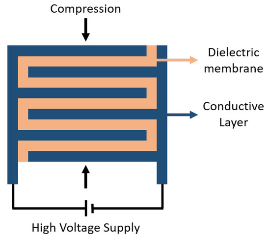
Figure 2.
Cross-sectional view of the stacked DEA structure. Interdigitated conductive layers are isolated from each other by the serpentine-shaped dielectric material between. On each side, alternating conductive layers are interconnected and attached to a power source. The actuator is compressed in the perpendicular direction (indicated by the arrows) when a voltage is applied and expands in the lateral direction.
In Figure 3a, an SEM image of a small cross-sectional area taken from the middle of a stacked DEA specimen, with a 50 m layer thickness, is shown. The darker layers are the dielectric PDMS layers and the lighter layers are c-PDMS (MWCNT/PDMS composite). Figure 4 shows a close-up of the conductive composite layer in the stacked actuator structure. The MWCNTs can be seen in the image as they are coming out of the PDMS matrix. Figure 3b shows a cross-sectional image of the stacked actuator that was imaged under the SEM and was edited in ImageJ [34] to provide a perspective on the MWCNT distribution in PDMS and layer uniformity in the actuator.
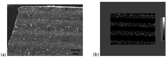
Figure 3.
(a) SEM image of a partial cross-sectional area of a stacked DEA sample with an average of 50 m layer thickness. (b) A different cross-sectional area of the same stacked actuator modified in ImageJ to highlight the MWCNT distribution in the actuator. Image from [19].
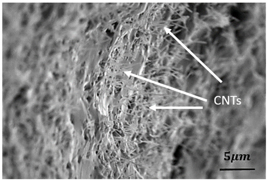
Figure 4.
SEM image of the cross-sectional area of the MWCNT/PDMS composite layer within the stacked actuator structure, zoomed at a shallow angle to highlight the presence of carbon nanotubes.
3.3. Microfabrication of Stacked DEAs
Once the proposed structure proved feasible for fabrication of “macro-scale” multi-layer DEAs, a “micro-scale” stacked DEA structure and a novel fabrication process were designed that incorporated of soft lithography tools. The biomimetically inspired stacked actuator consisted of interdigitated conductive layers, isolated with the dielectric PDMS, as shown in Figure 5. A photomask with 20 m thick interdigitated lines and electrode connections for the voltage input was designed.
Figure 5.
(a) Schematic of a single DEA structure with the dielectric membrane sandwiched between two parallel conductive layers; (b) schematic of a stacked DEA structure with many layers of alternating dielectric and conductive elastomers; (c) actual stacked DEA fabricated using a microfabrication approach; (d) microscope image of the interdigitated conductive elastomer layers in the photoresist mold.
For the photoresist molds, RCA cleaned 3-inch mechanical grade silicon wafers were coated with SU-8 photoresist at 1000 rpm for 30 s with a 500 rpm ramp of 5 s. Soft-bake step was done at 95 °C for 45 min, until the resist film stopped wrinkling when removed from the hotplate. Using the photomasks, the negative photoresist was exposed with UV for a total dose of 250 mJ/cm2 using Karl Suss MA 150 aligner, using an i-line filter. Post-exposure bake was started at 65 °C for 1 min and finished at 95 °C where the wafer was held for 5 min. The photoresist was developed with MicroChem SU-8 developer (MicroChem, Westborough, MA, USA) to wash away the uncured SU-8, rinsed with IPA (isopropyl alcohol), and dried. Patterned SU-8 films were hard-baked at 150 °C to improve the structural integrity of the relatively high-aspect-ratio features. The thickness of the SU-8 film and the height of the features were measured, using a KLA Tencor P2 profilometer (KLA-Tencor, Milpitas, CA, USA) as 180 m. Three different methods were investigated for the fabrication of micro-sized stacked actuators.
Originals and inverted (negative) versions of the same mask design were printed to use as the photomask for the different methods. For all the photoresist (negative and original) molds, the same fabrication procedure was followed. PDMS was prepared at a 15:1 base to curing agent ratio and c-PDMS was prepared at a 10:1 ratio, unless otherwise stated.
3.3.1. Method I
For Method I, the photoresist molds were fabricated using the original photomask. Figure 6 depicts each step of this fabrication approach. As shown in the figure, gray, blue, yellow, and black pieces represent the silicon wafer, photoresist, PDMS, and c-PDMS, respectively.
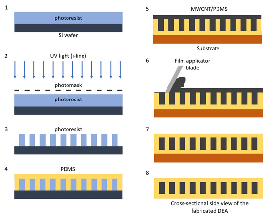
Figure 6.
Schematics for the process flow for microfabrication Method I. All images show cross-sectional side views of a small section of each material/tool used during the fabrication process.
The photoresist molds were coated with PDMS and cured at 80 °C for 30 min. The cured PDMS was peeled from the photoresist, which formed the interdigitated dielectric layers and the bottom PDMS layer. The structure was placed on a blank wafer and coated with c-PDMS to fill the gaps in the PDMS to form the conductive interdigitated layers and interconnections for each layer. The excess c-PDMS was removed using a combination of a metal blade and a custom film applicator blade with a PDMS coated edge to isolate individual conductive layers of the stacked DEA. The completed structure was cured and individual devices were cut to obtain free standing stacked fiber-like DEAs.
The schematic in Figure 7a shows the cross-sectional side view of the final structure as depicted in Step 8 in Figure 6, without the encapsulation layers at the top and the bottom. Figure 7b depicts the device at a distance as seen from a low-angle perpective. Figure 7c shows the same structure from the top, with the interdigitated conductive layers and the dielectric layers between them.
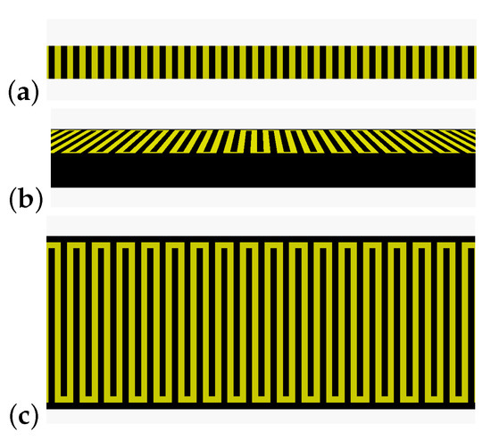
Figure 7.
Schematics showing the cross-sectional side view (a), a low-angle perspective (b), and a top view (c) of a stacked DEA structure with alternating layers of conductive (black) and dielectric (yellow) PDMS. Note that the image is not to scale.
It was observed that, when a softer dielectric material (with lower elastic modulus) was used for this method, it was more difficult to coat the c-PDMS onto and clean the excess solution from the PDMS dielectric layer. Due to the mechanical pressure from the cleaning step, high pillars (dielectric layers) tended to deform and collapse.
3.3.2. Method II
For the second approach, a similar fabrication method was followed. However, the negative photoresist molds were used for this approach, instead of the original pattern. Therefore, after the photoresist molds were prepared, the molds were coated with the c-PDMS mixture, as opposed to PDMS, as shown in Figure 8. The excess c-PDMS was removed using the same tools as in Method I.
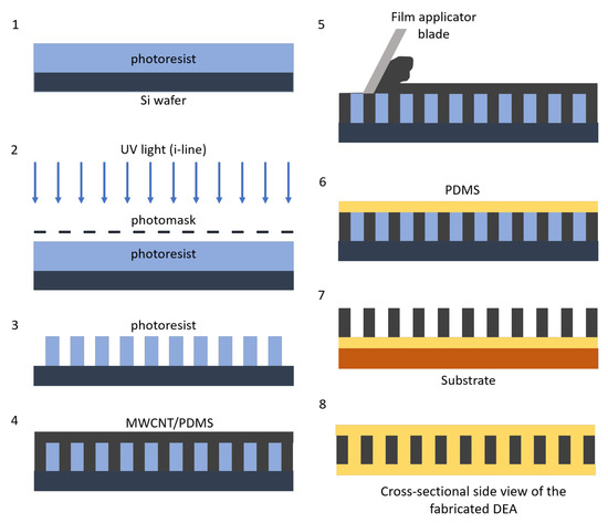
Figure 8.
Schematics for the process flow for Method II. Conductive layers are fabricated before the dielectric layers.
After curing the c-PDMS, it was coated with a 50 micron PDMS layer and cured again at 80 °C. Once the PDMS was solidified, the structure was peeled from the wafer (from the resist mold) and encapsulated with PDMS on the other side using the same curing procedure. Figure 7 shows a representative cross-sectional image of a stacked DEA after this step. Finally, devices were cut from the rest of the polymer and free-standing DEA fibers were obtained.
3.3.3. Method III—Injection
An alternative approach to coating the c-PDMS was to inject it into the dielectric structure using a syringe with fine tip needle that could deliver the c-PDMS into the fabricated dielectric structure. Figure 9 illustrates the fabrication approach via injection molding schematically. For this approach, the same masks used in Method I were used to fabricate the photoresist mold for forming the initial dielectric structure. The dielectric PDMS formed the serpentine structure and the interdigitated structure for the conductive layers was hollow.
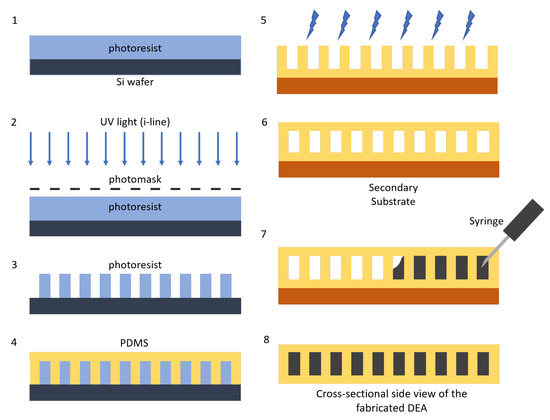
Figure 9.
Schematic depicting the process flow for the injection molding approach (Method III). Drawings in the figure are not to scale and represent the cross-sectional side views at the center of each structure.
The PDMS was spin-coated onto the resist mold and cured, then detached from the mold and placed on a flat surface (i.e., bare silicon wafer or glass substrate). Another PDMS layer was spin-coated on a blank wafer (with no mold) to form a thin and flat PDMS sheet. Once it was cured, the thin PDMS sheet was peeled from the silicon wafer. Both PDMS pieces (flat sheet and the patterned PDMS) were treated with a low-temperature corona discharge plasma (corona treatment) to functionalize the surfaces. The thin PDMS sheet was carefully placed on top of the patterned PDMS to cover the entire area and seal off all the hollow structures on the PDMS. The two attached pieces were placed in the oven to improve the bonding and baked at 95 °C for 30 min.
Sealed devices were cut from the bottom end in order to let the trapped air out during the injection process. The c-PDMS mixture was injected into the sealed devices to form the conductive DEA layers. However, it was observed that, depending on the viscosity of the c-PDMS mixture, internal pressure during the injection process caused breaking of the bonds between the PDMS layers and caused leaking. Therefore, sealed PDMS structures were placed in a vacuum chamber and the c-PDMS syringe was inserted into the hollow structure. Vacuum was used to remove the air inside the sealed devices and pull the c-PDMS mixture into the hollow regions.
Figure 10a shows the two pieces of PDMS sealed together after the corona treatment step. Two devices in the image were cut from the rest of the PDMS. The needle, attached to the syringe containing the c-PDMS mixture, is inserted into the hollow area that forms the electrode connection for the power input. Another needle is inserted from the opposite end, as shown in Figure 10b, to introduce vacuum into the chamber.
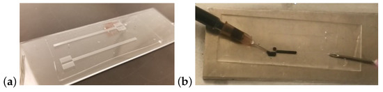
Figure 10.
(a) Two PDMS pieces sealed together to form the dielectric part of the stacked DEA structure before injecting the c-PDMS in Method III. (b) Injection of c-PDMS. The needle on the right-hand side of (b) is placed at the bottom end of the sealed device to let the air out easily from inside the hollow channels into the vacuum chamber.
4. Results
4.1. Actuation Test Results
Wires were attached to the fabricated devices by using c-PDMS to encapsulate and secure the connection points. The actuators were tested using a high-voltage power source, and voltages ranging from 500 V to 2 kV were applied.
Figure 11 shows the fabricated stacked dielectric elastomer actuators fabricated using Method I (a) and the same actuator in its actuated state (b). The actuation distance was calculated as the difference between the final and the initial position of the free-end of the actuator in perpendicular direction. The same method was applied to measure the actuation ratio of the fabricated devices using all three fabrication methods.
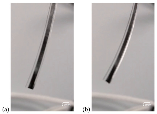
Figure 11.
(a) Representative single stacked actuator fabricated using Method I. (b) Microfabricated actuator in its actuated state.
Figure 12a through c show the average actuation ratios of the devices fabricated using Methods I, II, and III respectively. The results obtained through all three fabrication methods appear to follow a similar trend. Figure 12d shows a comparison of the actuation ratios of the microfabricated stacked DEAs (with dielectric layer thicknesses of 20 m) and compares the actuation ratio of microfabricated DEAs with the macro-scale DEAs (with dielectric layer thicknesses of 50 m) fabricated layer by layer. The values for the actuation of the 20 m actuator represent the average actuation values of all the devices fabricated through the different microfabrication approaches. Microfabricated DEAs were actuated at voltages between 0.5 and 1.2 kV. A maximum average actuation, which was observed with the samples fabricated through Method II, was measured at around 6.2% at 1.2 kV, after which point the devices failed due to dielectric breakdown.
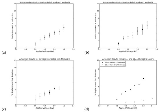
Figure 12.
Actuation results for the devices fabricated through (a) Method I, (b) Method II, and (c) Method III. (d) The actuation ratios of devices with dielectric layer thickness of 20 and 50 m. Error bars indicate the standard deviation of the measurements in (a, b) and indicate instrument accuracy in (c).
4.2. Discussion
Through this study, it was shown that, by utilizing different microfabrication tools and techniques, it is possible to fabricate free-standing stacked dielectric elastomer actuator structures. With the first two fabrication approaches, the main challenge was the removal of the excess c-PDMS from the surface after coating. This problem diminished the repeatability of the fabrication process. Applying a larger force helped remove the excess solution, but also damaged the mold and deformed the dielectric elastomer. Applying an additional high-speed spinning step (1000 rpm for 20 s) removed some of the excess material, but also resulted in an uneven filling of the features in some cases.
Figure 4 in [19] represents three different stacked DEAs fabricated through the same fabrication process (Method II) with slightly different parameters. The force applied for removal of the excess solution is larger and the spin coating speed is increased from a through c. Although 4c appears to depict what an ideal device should look like, there are local defects and non-uniformities throughout the device.
Using Method II, it is observed in Figure 11b that the actuation occurs as a combination of compression and bending. This is due to the difference in thickness of the PDMS layers on each side of the actuator. The compression force is more effective on one side of the actuator while it is inhibited by the counteracting stress caused by the thicker PDMS layer on the other side. This can be adjusted by fine-tuning the coating parameters on either side of the structure. When the thickness is uniform and equal on each side, the device should only contract, while it is also possible, as shown in the figure, to introduce a bending mechanism by changing the thickness on either side.
The injection method (Method III) was observed to work better than the two other methods, however only for a short injection distance. There may be a few possible ways to improve the injection method: (1) bonding between the two PDMS layers could be improved through a different surface treatment or functionalization, (2) a thinner PDMS could be used for preparing the conductive composite material, or (3) creating a negative pressure inside the microchannels by applying vacuum could help maintain the physical contact between the patterned structure and the top PDMS layer. An additional enhancement for the injection fabrication process could be done by using a micromanipulator to inject the conductive mixture into the channels in a more precise and accurate manner.
Fabricated actuators worked in the sub-kV range and exhibited 5–6% displacement. The data pattern in Figure 12 seems to follow the theoretical actuation trend defined by Equation (1) with some discrepancies. Equation (1) assumes ideal conditions for calculating the displacement of a DEA and neglects the counter-acting forces imposed by the dielectric encapsulation layers and the interconnections between conductive layers, which could explain the discrepancies between the theoretical calculations and the experimental results.
The applied voltage measured at the dielectric breakdown corresponds to a breakdown field of 60 MV/m. This value is within the same magnitude range reported by the manufacturer. Gerratt et al. showed that the breakdown field can change significantly with the dielectric geometry for PDMS thin films and they reported values higher than previously found in the literature [35]. Recently, there have also been studies investigating the electromechanical instabilities in soft dielectric elastomers [36,37]. It has been shown that the unstable domains are affected by a number of factors, including the amount of the stiffer phases in the material, direction of anisotropy in anisotropic systems, direction of the applied electric field relative to the inclusions in hybrid systems with periodic inclusions [36,37,38]. It has been suggested that the instabilities associated with finite deformation could also be exploited to improve the actuation. The effects of the device geometry, filler concentration, layer alignment on the dielectric properties of the fabricated devices should be studied to better understand the failure mechanisms and to improve the actuation performance.
The study presents how microfabrication tools can be used to fabricate biomimetic stacked EAP actuators composed of micro-sized DEA units, which can be utilized not only in micro-scale but also in macro-scale applications. Compared to previous studies in the literature, this approach allows the fabrication of free-standing linear actuators, the fabrication of hundreds of DEA layers in a single step instead of sequential fabrication of each layer, thus making the fabrication time independent of the number of layers, and provides a fabrication approach that can be used for scaling up multi-layer DEAs.
Future work should include a parametric study and the modeling of multi-layer DEAs that investigate the effect of the thickness and the elastic modulus of the dielectric encapsulation layer and conductive interconnections on actuation performance. The spacing between the dielectric and the conductive layers, and the ratio of dielectric layer thickness to conductive layers thickness, should also be optimized through a parametric study.
With lower input voltages, it is possible to utilize DEA actuators in soft robotic applications ranging from aerospace to biotechnology. The smaller fiber-like actuator structures could be connected to together to form larger and more complex artificial muscle structures, mimicking natural muscles, enhancing the force output, and enabling a wider range of motion.
Author Contributions
Data curation, M.C.; Funding acquisition, W.W. and K.L.-K.; Investigation, M.C.; Methodology, M.C. and K.L.-K.; Project administration, M.C. and K.L.-K.; Resources, K.L.-K.; Supervision, K.L.-K.; Writing original draft, M.C.; Writing, review and editing, K.L.-K.
Funding
This research was funded by Google Inc.
Conflicts of Interest
The authors declare no conflict of interest.
References
- Ilievski, F.; Mazzeo, A.D.; Shepherd, R.F.; Chen, X.; Whitesides, G.M. Soft Robotics for Chemists. Angew. Chem. Int. Ed. 2011, 50, 1890–1895. [Google Scholar] [CrossRef] [PubMed]
- Wehner, M.; Truby, R.L.; Fitzgerald, D.J.; Mosadegh, B.; Whitesides, G.M.; Lewis, J.A.; Wood, R.J. An integrated design and fabrication strategy for entirely soft, autonomous robots. Nature 2016, 536, 451–455. [Google Scholar] [CrossRef] [PubMed]
- Bauer, S.; Bauer-Gogonea, S.; Graz, I.; Kaltenbrunner, M.; Keplinger, C.; Schwödiauer, R. 25th Anniversary Article: A Soft Future: From Robots and Sensor Skin to Energy Harvesters. Adv. Mater. 2014, 26, 149–162. [Google Scholar] [CrossRef] [PubMed]
- Bar-Cohen, Y. Electro-active polymers: current capabilities and challenges. In Proceedings of the Smart Structures and Materials 2002: Electroactive Polymer Actuators and Devices, San Diego, CA, USA, 17–21 March 2002; Volume 4695, pp. 1–7. [Google Scholar]
- Biggs, J.; Danielmeier, K.; Hitzbleck, J.; Krause, J.; Kridl, T.; Nowak, S.; Orselli, E.; Quan, X.; Schapeler, D.; Sutherland, W.; et al. Electroactive Polymers: Developments of and Perspectives for Dielectric Elastomers. Angew. Chem. Int. Ed. 2013, 52, 9409–9421. [Google Scholar] [CrossRef] [PubMed]
- Pelrine, R. High-Speed Electrically Actuated Elastomers with Strain Greater Than 100%. Science 2000, 287, 836–839. [Google Scholar] [CrossRef] [PubMed]
- Rosset, S.; Shea, H.R. Small, fast, and tough: Shrinking down integrated elastomer transducers. Appl. Phys. Rev. 2016, 3, 031105. [Google Scholar] [CrossRef]
- Kovacs, G.; Düring, L.; Michel, S.; Terrasi, G. Stacked dielectric elastomer actuator for tensile force transmission. Sens. Actuators A Phys. 2009, 155, 299–307. [Google Scholar] [CrossRef]
- Bar-cohen, Y. Electroactive Polymer (EAP) Actuators as Artificial Muscles Reality, Potential, and Challenges; SPIE Press: Bellingham, WA, USA, 2004; pp. 1–14. [Google Scholar]
- Balakrisnan, B.; Smela, E. Challenges in the Microfabrication of Dielectric Elastomer Actuators. Electroact. Polym. Actuators Devices 2010, 7642. [Google Scholar] [CrossRef]
- Hines, L.; Petersen, K.; Lum, G.Z.; Sitti, M. Soft Actuators for Small-Scale Robotics. Adv. Mater. 2017, 29. [Google Scholar] [CrossRef] [PubMed]
- Dubois, P.; Rosset, S.; Koster, S.; Stauffer, J.; Mikhaïlov, S.; Dadras, M.; de Rooij, N.F.; Shea, H. Microactuators based on ion implanted dielectric electroactive polymer (EAP) membranes. Sens. Actuators A Phys. 2006, 130–131, 147–154. [Google Scholar] [CrossRef]
- Gerratt, A.P.; Balakrisnan, B.; Penskiy, I.; Bergbreiter, S. Batch fabricated bidirectional dielectric elastomer actuators. In Proceedings of the 2011 16th International Solid-State Sensors, Actuators and Microsystems Conference, TRANSDUCERS’11, Beijing, China, 5–9 June 2011; pp. 2422–2425. [Google Scholar]
- Poulin, A.; Rosset, S.; Shea, H.R. Printing low-voltage dielectric elastomer actuators. Appl. Phys. Lett. 2015, 107. [Google Scholar] [CrossRef]
- Duduta, M.; Wood, R.J.; Clarke, D.R. Multilayer Dielectric Elastomers for Fast, Programmable Actuation without Prestretch. Adv. Mater. 2016, 28, 8058–8063. [Google Scholar] [CrossRef] [PubMed]
- McCoul, D.; Rosset, S.; Schlatter, S.; Shea, H. Inkjet 3D printing of UV and thermal cure silicone elastomers for dielectric elastomer actuators. Smart Mater. Struct. 2017, 26. [Google Scholar] [CrossRef]
- Ji, X.; El Haitami, A.; Sorba, F.; Rosset, S.; Nguyen, G.T.; Plesse, C.; Vidal, F.; Shea, H.R.; Cantin, S. Stretchable composite monolayer electrodes for low voltage dielectric elastomer actuators. Sens. Actuators B Chem. 2018, 261, 135–143. [Google Scholar] [CrossRef]
- Corbaci, M.; Walter, W.; Lamkin-Kennard, K. Microfabrication of stacked dielectric elastomer actuator fibers. Electroact. Polym. Actuators Devices 2016, 9798, 979823. [Google Scholar] [CrossRef]
- Corbaci, M.; Lamkin-Kennard, K.; Walter, W. Optimization study for fabrication of micro-scale stacked dielectric elastomer actuators. In Proceedings of the SPIE 10163, Electroactive Polymer Actuators and Devices (EAPAD), Portland, OR, USA, 25–29 March 2017; Volume 101631I, p. 101631I. [Google Scholar]
- Kofod, G. Dielectric Elastomer Actuators. Ph.D. Thesis, The Technical University of Denmark, Copenhagen, Denmark, 2001. [Google Scholar]
- Romasanta, L.; Lopez-Manchado, M.; Verdejo, R. Increasing the performance of dielectric elastomer actuators: A review from the materials perspective. Prog. Polym. Sci. 2015, 51, 188–211. [Google Scholar] [CrossRef]
- Rosset, S.; Shea, H.R. Flexible and stretchable electrodes for dielectric elastomer actuators. Appl. Phys. A 2013, 110, 281–307. [Google Scholar] [CrossRef]
- Bar-Cohen, Y. Electroactive Polymers as Artificial Muscles - Reality and Challenges. Adv. Piezoelectr. Mater. 2001, 1–13. [Google Scholar] [CrossRef]
- Akbari, S.; Rosset, S.; Shea, H.R. Improved electromechanical behavior in castable dielectric elastomer actuators. Appl. Phys. Lett. 2013, 102, 071906. [Google Scholar] [CrossRef]
- Dünki, S.J.; Ko, Y.S.; Nüesch, F.A.; Opris, D.M. Self-Repairable, High Permittivity Dielectric Elastomers with Large Actuation Strains at Low Electric Fields. Adv. Funct. Mater. 2015, 25, 2467–2475. [Google Scholar] [CrossRef]
- Liu, C.X.; Choi, J.W. Strain-dependent resistance of PDMS and carbon nanotubes composite microstructures. IEEE Trans. Nanotechnol. 2010, 9, 590–595. [Google Scholar] [CrossRef]
- Shao, G.; Wu, J.; Cai, Z.; Wang, W. Fabrication of elastomeric high-aspect-ratio microstructures using polydimethylsiloxane (PDMS) double casting technique. Sens. Actuators A Phys. 2012, 178, 230–236. [Google Scholar] [CrossRef]
- Deman, A.L.; Brun, M.; Quatresous, M.; Chateaux, J.F.; Frenea-Robin, M.; Haddour, N.; Semet, V.; Ferrigno, R. Characterization of C-PDMS electrodes for electrokinetic applications in microfluidic systems. J. Micromech. Microeng. 2011, 21, 1–8. [Google Scholar] [CrossRef]
- Johnston, I.D.; McCluskey, D.K.; Tan, C.K.L.; Tracey, M.C. Mechanical characterization of bulk Sylgard 184 for microfluidics and microengineering. J. Micromech. Microeng. 2014, 24, 035017. [Google Scholar] [CrossRef]
- Cotton, D.P.J.; Popel, A.; Graz, I.M.; Lacour, S.P. Photopatterning the mechanical properties of polydimethylsiloxane films. J. Appl. Phys. 2011, 109, 054905. [Google Scholar] [CrossRef]
- Araromi, O.A.; Rosset, S.; Shea, H.R. High-Resolution, Large-Area Fabrication of Compliant Electrodes via Laser Ablation for Robust, Stretchable Dielectric Elastomer Actuators and Sensors. ACS Appl. Mater. Interfaces 2015, 7, 18046–18053. [Google Scholar] [CrossRef] [PubMed]
- Andrews, R.; Weisenberger, M. Carbon nanotube polymer composites. Curr. Opin. Solid State Mater. Sci. 2004, 8, 31–37. [Google Scholar] [CrossRef]
- Liu, C.X.; Choi, J.W. Patterning conductive PDMS nanocomposite in an elastomer using microcontact printing. J. Micromech. Microeng. 2009, 19, 085019. [Google Scholar] [CrossRef]
- Schneider, C.A.; Rasband, W.S.; Eliceiri, K.W. NIH Image to ImageJ: 25 years of image analysis. Nature Methods 2012, 9, 671–675. [Google Scholar] [CrossRef] [PubMed]
- Gerratt, A.P.; Bergbreiter, S. Dielectric breakdown of PDMS thin films. J. Micromech. Microeng. 2013, 23, 067001. [Google Scholar] [CrossRef]
- Rudykh, S.; DeBotton, G. Stability of anisotropic electroactive polymers with application to layered media. Z. Angew. Math. Phys. 2011, 62, 1131–1142. [Google Scholar] [CrossRef]
- Rudykh, S.; Bhattacharya, K.; DeBotton, G. Multiscale instabilities in soft heterogeneous dielectric elastomers. Proc. R. Soc. A 2014, 470. [Google Scholar] [CrossRef] [PubMed]
- Goshkoderia, A.; Rudykh, S. Electromechanical macroscopic instabilities in soft dielectric elastomer composites with periodic microstructures. Eur. J. Mech. A. Solids 2017, 65, 243–256. [Google Scholar] [CrossRef]


© 2018 by the authors. Licensee MDPI, Basel, Switzerland. This article is an open access article distributed under the terms and conditions of the Creative Commons Attribution (CC BY) license (http://creativecommons.org/licenses/by/4.0/).