1. Introduction
As the applications of industrial robots, collaborative robots, and service robots continue to expand, motor technologies capable of simultaneously achieving high torque density, compact size, lightweight characteristics, and precise control performance are increasingly required for robotic joint drive systems. In particular, robotic joints require motors, gear reducers, sensors, and drive controllers to be integrated within highly limited spaces [
1,
2]. Therefore, thin motor structures capable of minimizing axial length while maintaining high torque characteristics have become increasingly important. In response to these demands, Axial Flux Permanent Magnet Motors (AFPMs), which can achieve higher torque density in thin structures compared to conventional Radial Flux Permanent Magnet Motors (RFPMs), have attracted considerable attention in space-constrained applications such as robotic joints [
3,
4,
5].
AFPMs have a disk-shaped structure in which the rotor and stator are axially aligned, and the magnetic flux is formed parallel to the rotational axis. Owing to this structural characteristic, AFPMs can achieve superior space utilization under identical volume conditions while effectively utilizing the outer diameter region to realize high torque density. Consequently, AFPMs are being actively studied for applications requiring limited axial dimensions, including robotic joints, drones, in-wheel systems, and Urban Air Mobility (UAM) [
6,
7,
8,
9].
AFPMs can be classified into slotted and slotless structures according to the stator configuration. Slotted AFPMs can achieve high electric loading and output density by concentrating magnetic flux through stator teeth. However, magnetic interactions between the stator teeth and permanent magnets inevitably generate cogging torque, vibration, and acoustic noise. In addition, a certain amount of axial space is required to accommodate the windings, making it difficult to realize extremely thin motor structures [
10,
11,
12,
13].
To overcome these limitations, slotless Printed Circuit Board (PCB)-based AFPMs have recently attracted significant attention.
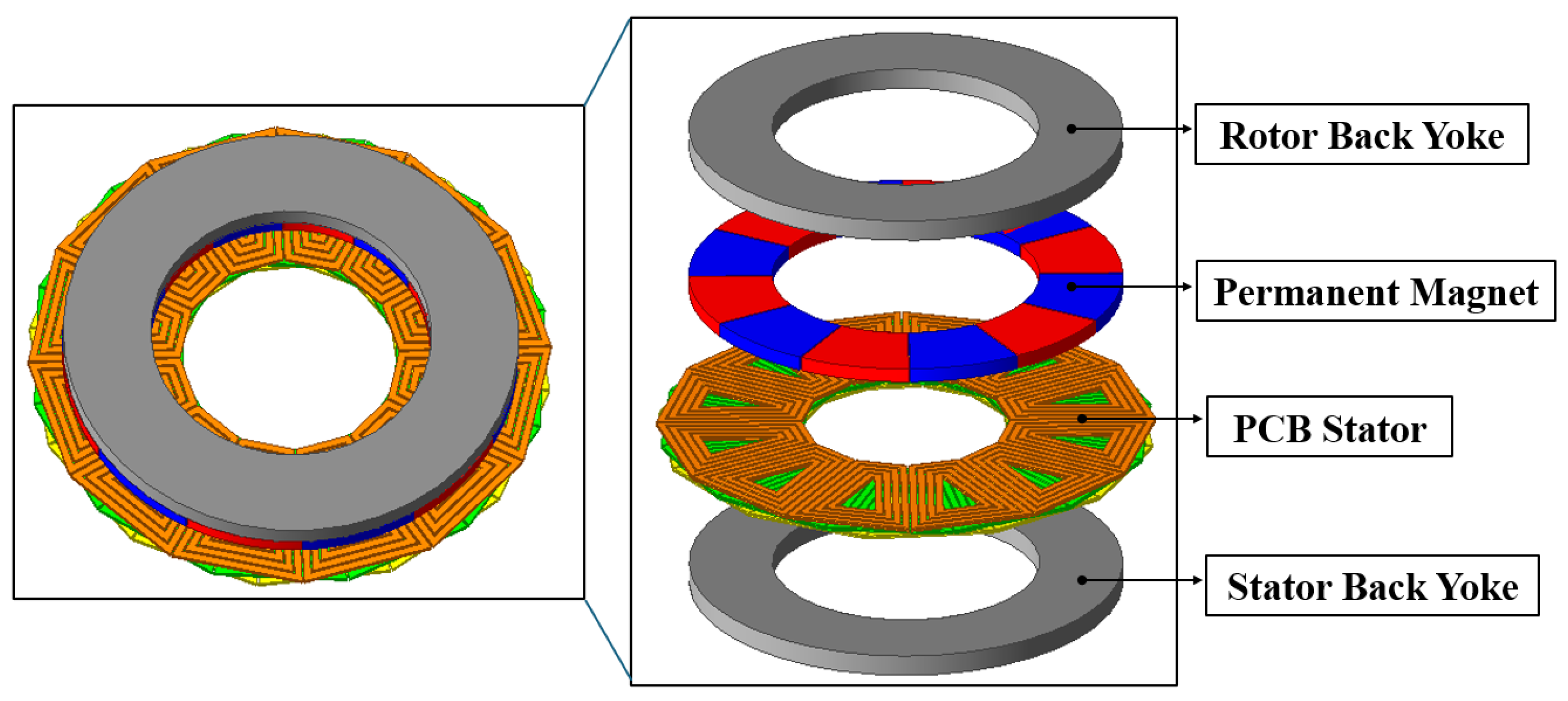
Figure 1 shows an AFPM equipped with a PCB stator. In PCB AFPMs, conventional stator teeth and copper windings are replaced with multilayer PCB conductor patterns. Since the winding patterns are fabricated through PCB etching processes, the manufacturing process can be significantly simplified compared to conventional winding structures. In addition, the absence of separate winding insertion and winding processes improves production repeatability and provides advantages in manufacturing automation and mass production [
14,
15,
16].
Furthermore, multilayer PCB structures provide high design flexibility because conductor patterns, series turn configurations, and phase connections can be precisely designed within limited spaces. In particular, the thin copper and insulation layer structure of PCBs enables extremely short axial lengths, making PCB AFPMs suitable for robotic joint drive systems requiring compact and thin structures. Moreover, PCB windings can be designed such that the end-turn regions are directly exposed to the housing or cooling structures, enabling superior thermal performance through direct end-turn cooling. This structural characteristic effectively suppresses winding temperature rise and allows relatively high current density operation compared to conventional slotted winding structures [
17,
18].
In addition, PCB AFPMs adopt a slotless structure without stator teeth, fundamentally eliminating cogging torque caused by magnetic interactions between the stator teeth and permanent magnets. As a result, PCB AFPMs exhibit reduced vibration and acoustic noise, making them highly advantageous for robotic joint systems requiring smooth rotation and precise low-speed control.
However, concentrated winding patterns are generally adopted in PCB AFPMs to maximize winding factor and series turn count within limited PCB space. Although concentrated winding structures are advantageous for achieving high flux linkage, the end-turns and closed current paths of each phase are distributed at different axial positions in single-rotor structures. As a result, differences in effective airgap and magnetic flux linkage occur among phases, leading to back-EMF imbalance.
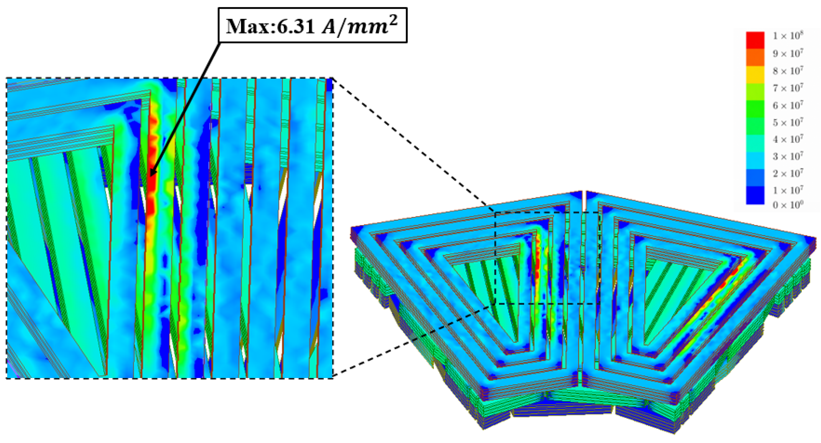
In addition, PCB conductors consist of wide and thin planar structures directly exposed to the time-varying magnetic field generated by permanent magnets, which increases AC losses caused by eddy current and proximity effects. In particular, back-EMF imbalance induces localized current concentration in specific phase conductors, resulting in additional AC losses and local heating. These phenomena can degrade overall efficiency, increase torque ripple, and reduce control stability [
19,
20].
Previous studies have attempted to reduce PCB winding losses by modifying the conductor width, thickness, or winding geometry. Although these approaches are effective for reducing losses, they usually require changes in the physical dimensions or manufacturing specifications of the PCB conductors. In contrast, this study focuses on reducing AC loss and improving phase balance by rearranging the layer-wise winding sequence while maintaining the same conductor thickness and overall motor geometry [
21,
22].
Therefore, this paper investigates the phase-dependent flux-linkage imbalance inherent in single-rotor concentrated-winding PCB AFPMs and identifies the limitations of conventional phase rearrangement approaches, particularly the phase resistance imbalance caused by unequal via-hole lengths. To address these issues, a layer-wise asymmetric turn distribution strategy is proposed, which compensates for the flux-linkage differences among phases while maintaining both the original phase arrangement and the total number of turns per slot per phase. Consequently, the proposed method simultaneously improves back-EMF balance and reduces AC loss without introducing phase resistance imbalance. The effectiveness of the proposed approach is validated through three-dimensional finite element analysis (FEA).
3. Modification of Conductor Arrangement for Each Phase
3.1. Example of Phase Rearrangement While Maintaining the Number of Turns
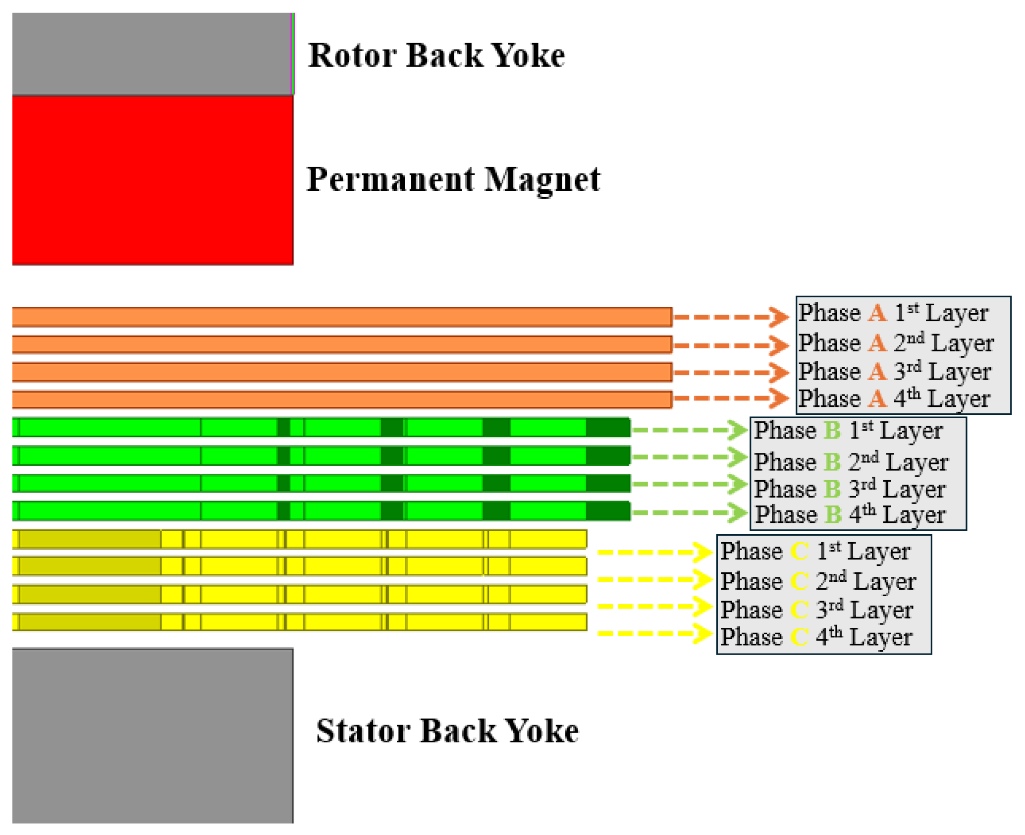
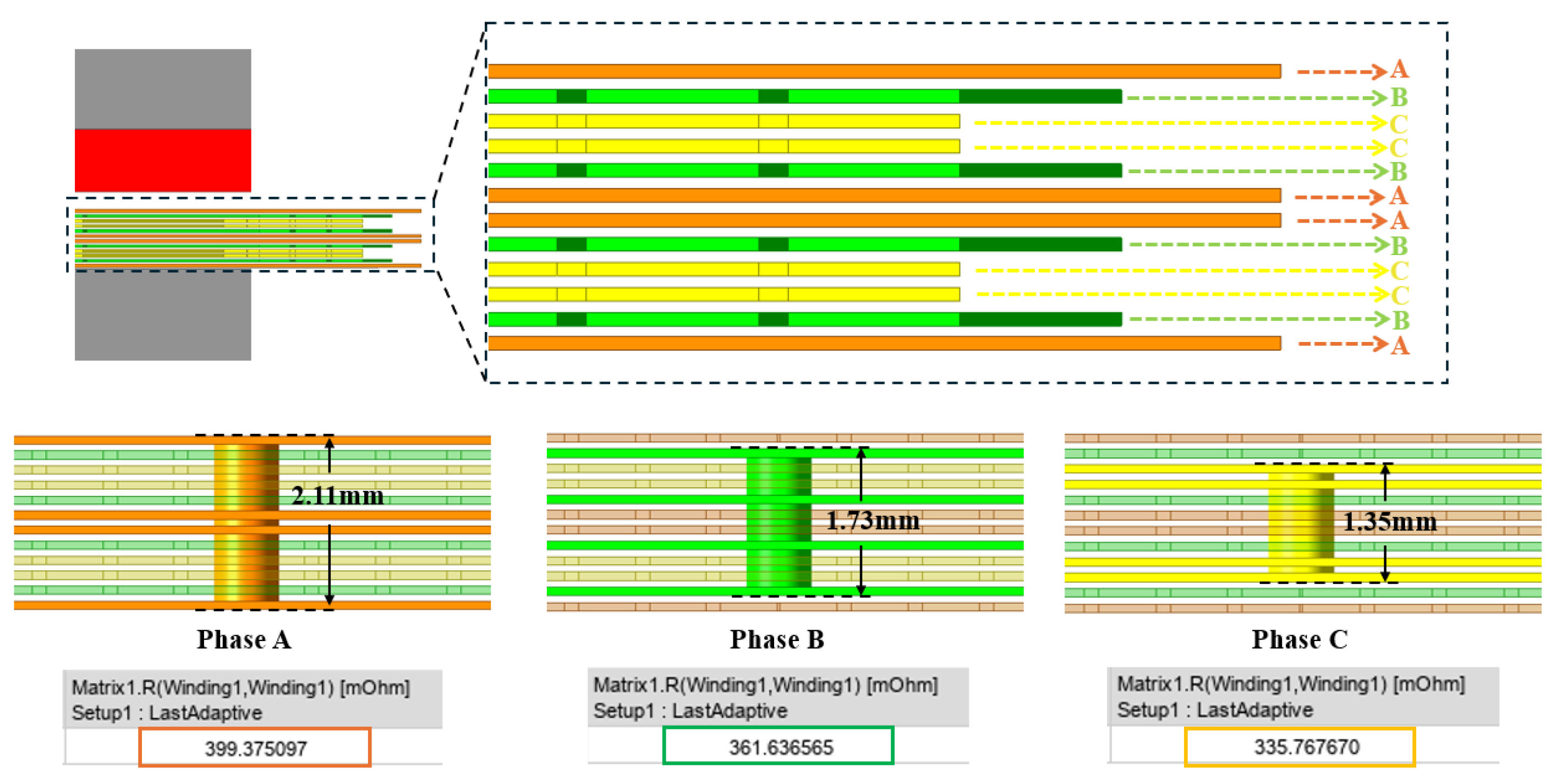
Figure 8 illustrates the phase arrangement modification applied to mitigate the back-EMF imbalance in the conventional concentrated winding PCB AFPM, as well as the resulting differences in via-hole lengths. In the conventional model, each phase is sequentially arranged along the PCB stacking direction, resulting in different distances between the permanent magnets and the closed current paths of each phase. Consequently, unequal magnetic flux linkage among the phases leads to back-EMF imbalance. To alleviate this issue, the phase arrangement was modified to an ABCCBA configuration, as shown in
Figure 8. This arrangement distributes each phase more uniformly along the PCB stacking direction, thereby equalizing the average distance between the permanent magnets and each phase. As a result, the variation in magnetic flux linkage among the phases can be reduced, leading to improved back-EMF balance.
However, the current flow characteristics of the concentrated winding PCB pattern introduce a new challenge. As described in
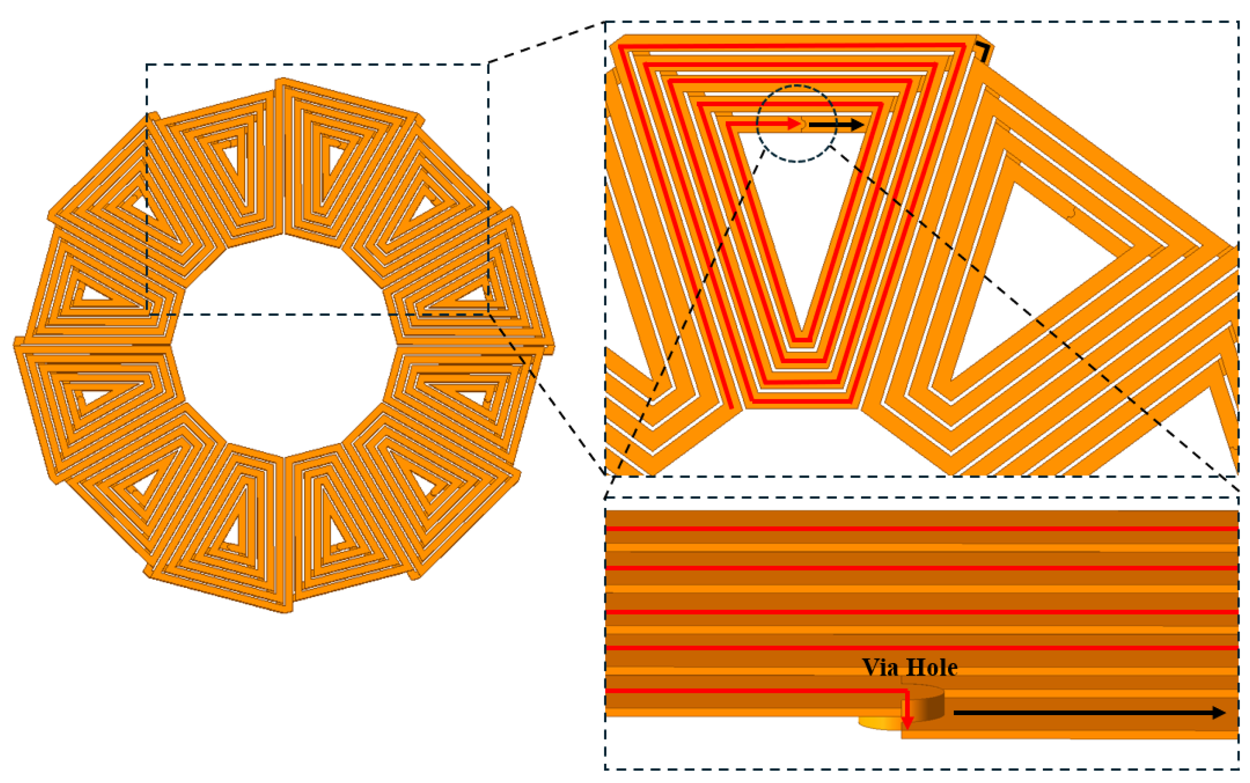
Figure 2, the current flows from the outer diameter toward the inner diameter in the first layer, transfers to the next layer through a via hole, and then flows back toward the outer diameter. Therefore, via holes are required to connect adjacent layers belonging to the same phase.
When the ABCCBA arrangement is applied, the layers belonging to the same phase are no longer continuously stacked. Consequently, the via-hole lengths become different for each phase. The via-hole lengths of Phase A, Phase B, and Phase C are approximately 2.11 mm, 1.73 mm, and 1.35 mm, respectively. As a result, the phase resistances were calculated as 399.38 mΩ, 361.64 mΩ, and 335.77 mΩ for Phases A, B, and C, respectively. A resistance difference of approximately 18.9% was observed between the highest-resistance phase (Phase A) and the lowest-resistance phase (Phase C).
Since the via hole forms part of the conductor path through which current flows, an increase in via-hole length inevitably increases the total conductor path length and, consequently, the electrical resistance. Therefore, the difference in via-hole lengths directly results in phase resistance imbalance. Such phase resistance imbalance can cause unequal phase currents under the same applied voltage condition, leading to current concentration in specific phases, additional copper losses, and localized heating. Furthermore, it may increase torque ripple and degrade current control performance. Therefore, phase resistance imbalance should be considered as an important design factor, comparable to the back-EMF imbalance itself.
Consequently, although the ABCCBA phase arrangement is effective in mitigating back-EMF imbalance, it simultaneously introduces a new issue in the form of phase resistance imbalance. Therefore, an additional conductor arrangement strategy is required to simultaneously achieve both back-EMF balance and phase resistance balance.
3.2. Examples of Asymmetric Conductor Arrangement with Modified Turn Counts
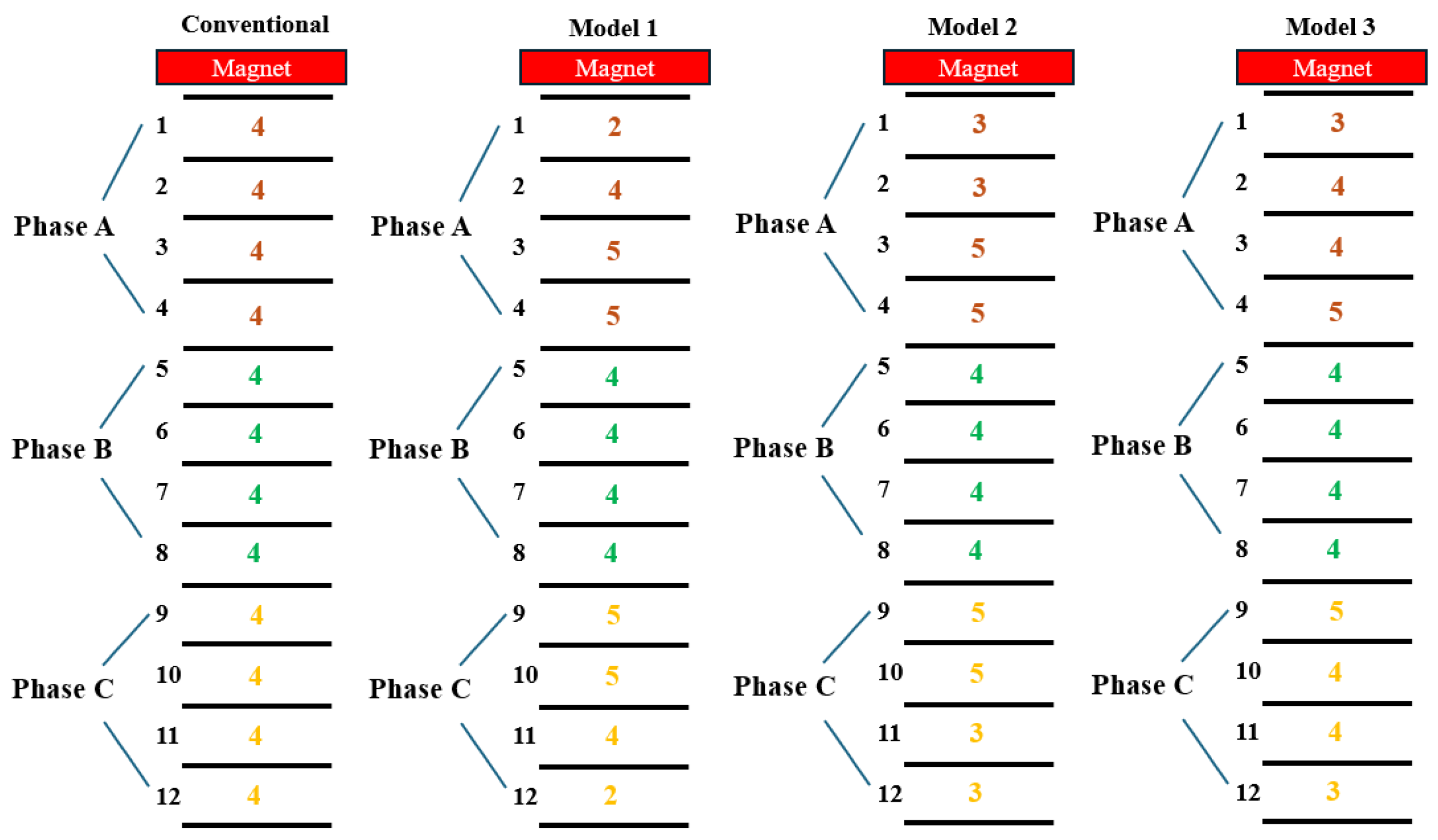
Figure 9 illustrates the asymmetric turn distribution models while maintaining the original AABBCC phase arrangement. As discussed in
Section 3.1, the ABCCBA phase arrangement can reduce back-EMF imbalance, but it may cause phase resistance imbalance due to unequal via-hole lengths. Therefore, this section introduces an asymmetric turn distribution method that maintains the original AABBCC phase arrangement while compensating for the layer-dependent flux-linkage difference.
In the conventional model, the equivalent number of turns per slot per phase is 16 turns, with four turns uniformly assigned to each of the four layers. However, in a single-rotor PCB AFPM, the layers closer to the permanent magnets experience larger magnetic flux linkage, whereas the layers farther from the magnets experience relatively smaller flux linkage. Therefore, uniform turn allocation does not necessarily result in balanced phase flux linkage.
where
is the phase back-EMF,
is the electrical angular velocity,
is the phase flux linkage,
is the number of turns assigned to the
i-th PCB layer, and
is the effective flux linkage per turn in the
i-th layer.
In the conventional model, the same number of turns is assigned to each layer. However, because varies depending on the axial layer position, uniform turn allocation does not necessarily result in balanced phase flux linkage. Therefore, the phase located closer to the permanent magnets obtains excessive back-EMF, whereas the phase located farther from the magnets obtains insufficient back-EMF.
Based on this principle, the proposed method redistributes the turn count of each layer while maintaining the same total number of turns per phase. The number of turns in high-flux-linkage layers is reduced to suppress excessive back-EMF, whereas the number of turns in relatively low-flux-linkage layers is increased to compensate for insufficient back-EMF. Therefore, the proposed layer-wise turn redistribution can be regarded as a flux-linkage compensation method rather than a simple heuristic modification of the winding pattern.
To mitigate this imbalance, the turns per slot per phase were maintained at 16 turns, while only the turn distribution within each phase was modified. Based on these constraints, three candidate models were selected to represent different compensation intensities. Model 1 applies the strongest compensation by reducing the turn count in the high-flux-linkage layers and increasing it in the lower-flux-linkage layers. Model 2 applies a grouped compensation strategy by dividing the layers into upper and lower regions. Model 3 applies a gradual compensation strategy to reduce abrupt changes in conductor distribution. In Model 1, Phase A was configured as 2–4–5–5 turns, Phase B as 4–4–4–4 turns, and Phase C as 5–5–4–2 turns. In Model 2, Phase A was configured as 3–3–5–5 turns, Phase B as 4–4–4–4 turns, and Phase C as 5–5–3–3 turns. In Model 3, Phase A was configured as 3–4–4–5 turns, Phase B as 4–4–4–4 turns, and Phase C as 5–4–4–3 turns. In all three models, the total turn number of turns per slot per phase was kept constant at 16 turns.
The purpose of this design is not to increase or decrease the total number of turns, but to adjust the effective conductor area linked by the permanent magnet flux in each layer. In other words, the turn count in the upper layers of Phase A, where the flux linkage is relatively large, was reduced to suppress excessive back-EMF. Conversely, in Phase C, the turn count was increased in the layers where relatively larger flux linkage can be obtained, in order to compensate for the insufficient back-EMF. Since Phase B is located in the middle region and has an intermediate flux linkage level, the reference turn distribution of 4–4–4–4 was maintained.
Model 1 applies the largest turn-count variation and is intended to strongly compensate for the back-EMF difference between Phases A and C. Model 2 divides the upper and lower layers of Phases A and C into two groups and adjusts the turn count accordingly, considering both compensation effectiveness and pattern feasibility. Model 3 applies a more gradual turn-count variation among layers, aiming to mitigate back-EMF imbalance while reducing abrupt changes in conductor width and current path.
Consequently, the proposed asymmetric turn distribution maintains the original AABBCC phase arrangement, thereby avoiding the long via holes and phase resistance imbalance that can occur in the ABCCBA arrangement. At the same time, by adjusting the turn count of each layer, the effective flux linkage of each phase can be compensated, resulting in improved back-EMF balance. Therefore, this design can be regarded as a conductor arrangement method for improving back-EMF balance while maintaining phase resistance balance.
The phase resistance values of the conventional and proposed conductor arrangements are compared in
Table 3. The resistance imbalance ratio was calculated using the difference between the maximum and minimum phase resistances normalized by the average phase resistance. In the conventional AABBCC arrangement, the phase resistance imbalance was negligible because each phase had nearly identical via-hole lengths. In contrast, the conventional ABCCBA arrangement exhibited a resistance imbalance of 17.40%, which was caused by the unequal via-hole lengths required to connect non-adjacent layers belonging to the same phase. The proposed models maintained the original AABBCC phase arrangement and therefore avoided additional via-hole length differences. As a result, the resistance imbalance ratios of Proposed Models 1, 2, and 3 were limited to 0.68%, 0.25%, and 0.44%, respectively. These results confirm that the proposed asymmetric turn distribution can improve back-EMF balance without introducing significant phase resistance imbalance.
4. FEA and Performance Analysis
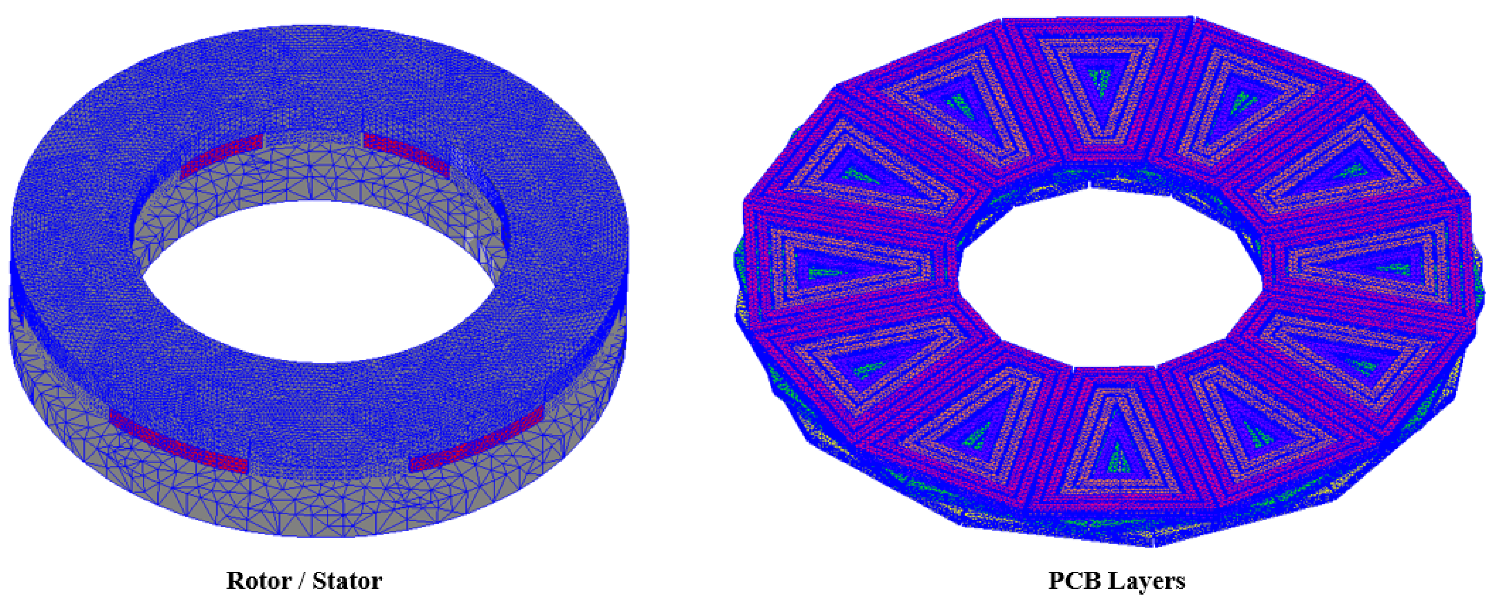
Figure 10 illustrates the mesh distribution used for the FEA. To achieve a balance between computational accuracy and simulation time, different mesh sizes were assigned to each component. In particular, the air-gap region, where significant magnetic field variation occurs, was assigned the finest mesh because it has the greatest influence on the electromagnetic analysis results.
The mesh size of the air-gap region was set to 0.8 mm, while mesh sizes of 4 mm and 5 mm were applied to the permanent magnets and both the rotor and stator cores, respectively. In addition, a mesh size of 1 mm was assigned to the PCB stator region to accurately represent the electromagnetic characteristics of the multilayer PCB winding structure. Since the PCB conductors directly interact with the magnetic flux generated by the permanent magnets and strongly influence the accuracy of back-EMF and AC loss calculations, a finer mesh was employed compared to the core regions.
As shown in
Figure 10, relatively uniform meshes were applied to the rotor and stator core regions, whereas denser meshes were assigned to the PCB winding and air-gap regions. This mesh configuration enables accurate analysis of localized electromagnetic phenomena, including back-EMF imbalance, current density distribution, and AC loss characteristics. Furthermore, all models were analyzed using identical mesh conditions to ensure that the observed performance differences originated from the design modifications rather than mesh-related effects.
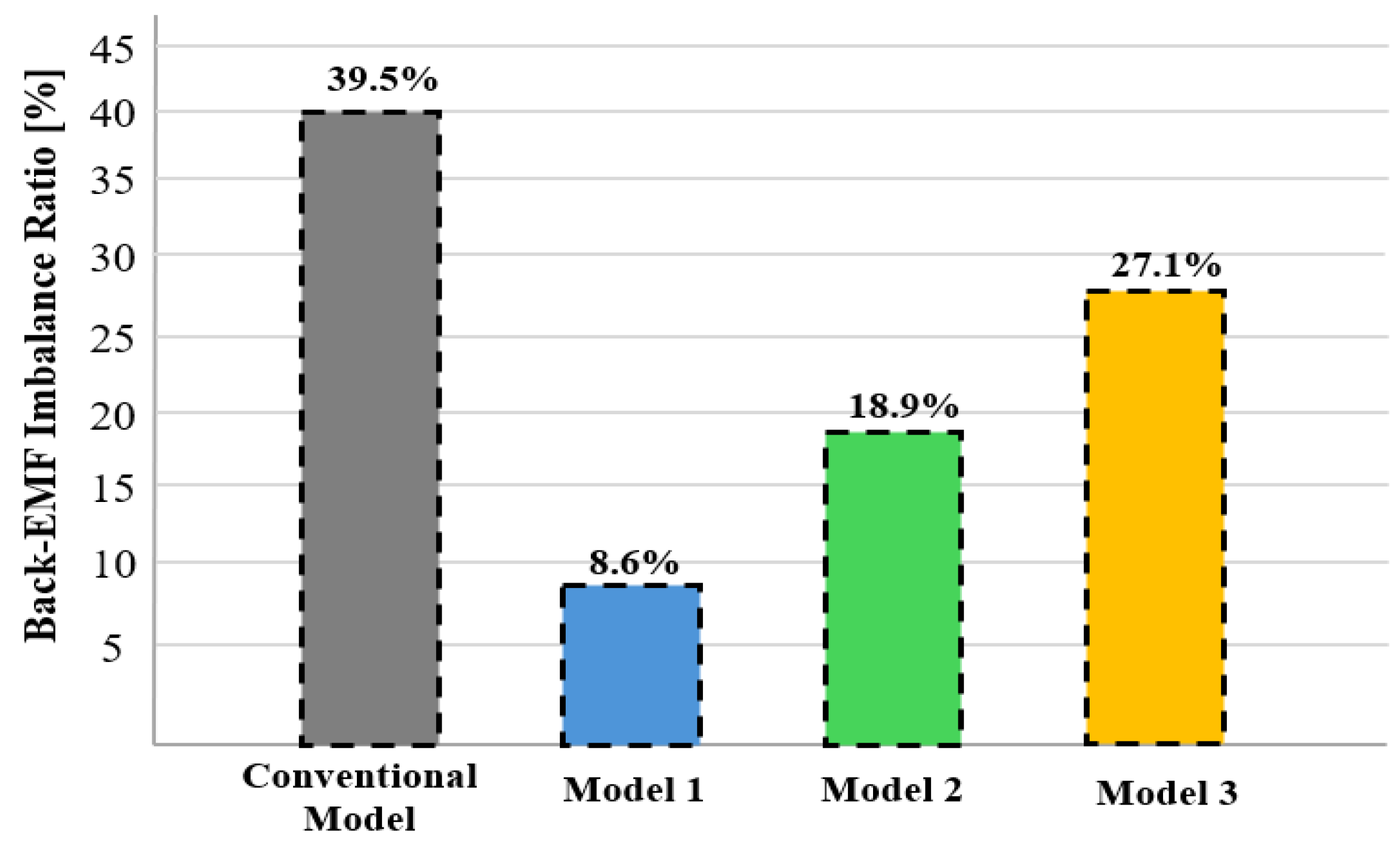
Figure 11 compares the back-EMF imbalance ratios of the proposed asymmetric turn distribution models, while
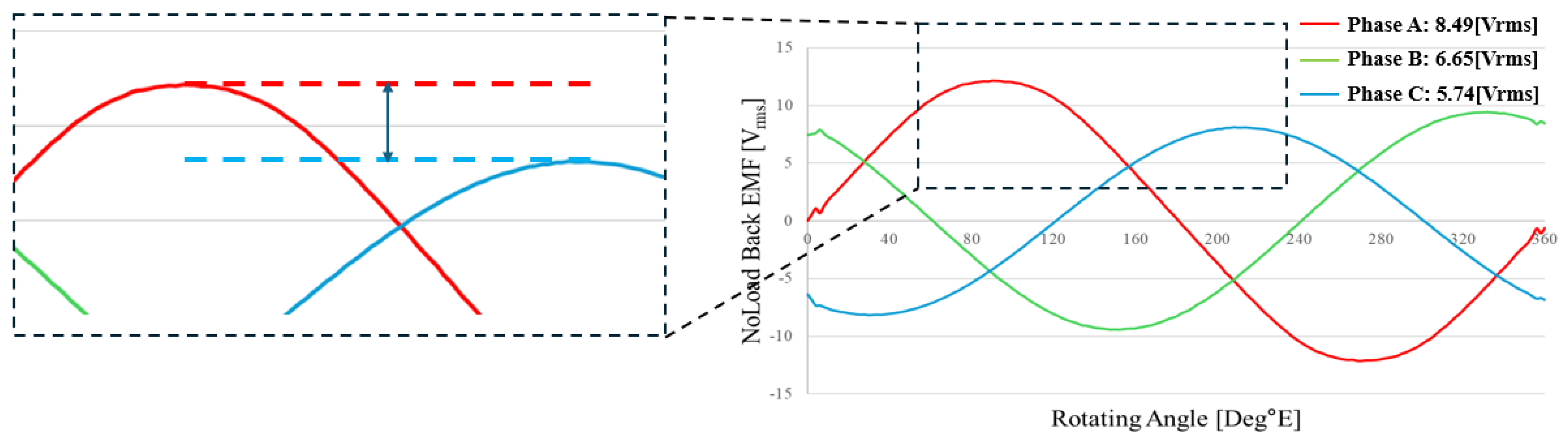
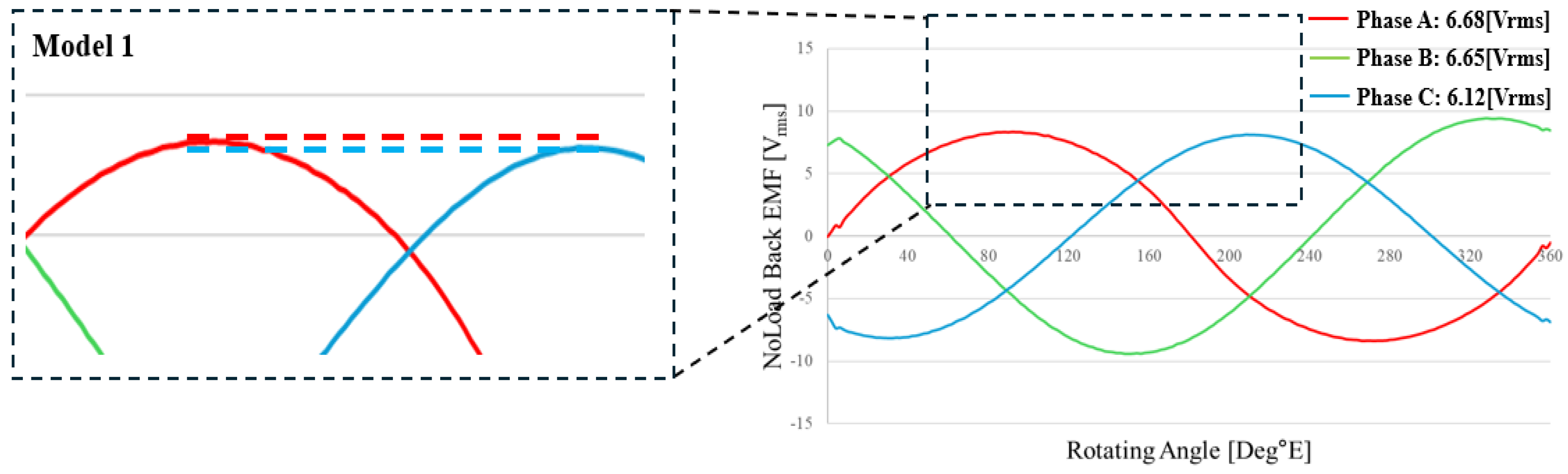
Figure 12 presents the no-load back-EMF waveforms of Model 1, which exhibited the best performance. As previously described, Model 1 employs turn distributions of 2–4–5–5 turns for Phase A, 4–4–4–4 turns for Phase B, and 5–5–4–2 turns for Phase C. Although the total number of turns per slot per phase was maintained at 16 turns, identical to the conventional model, the total turns per slot per phase of each layer was asymmetrically redistributed. This approach was intended to reduce excessive flux linkage in layers located close to the permanent magnets while increasing the effective flux linkage contribution of layers experiencing relatively lower magnetic flux.
As shown in
Figure 11, the conventional model exhibited a back-EMF imbalance ratio of 39.5%, whereas Model 2 and Model 3 showed imbalance ratios of 18.9% and 27.1%, respectively. In contrast, Model 1 achieved the lowest imbalance ratio of 8.6%, demonstrating the best back-EMF balancing performance among the proposed models. Compared with the conventional model, Model 1 reduced the back-EMF imbalance by approximately 78.2%, indicating that the proposed turn distribution effectively compensates for the flux-linkage differences among phases.
The same tendency can be observed in the no-load back-EMF waveforms shown in
Figure 12. In the conventional model, the back-EMF values of Phases A, B, and C were 8.49 Vrms, 6.65 Vrms, and 5.74 Vrms, respectively, indicating a significant phase-to-phase variation. In contrast, Model 1 produced back-EMF values of 6.68 Vrms, 6.65 Vrms, and 6.12 Vrms for Phases A, B, and C, respectively, significantly reducing the amplitude difference among phases. In particular, the back-EMF of Phase A, which originally exhibited the highest value, decreased, while the back-EMF of Phase C, which originally exhibited the lowest value, increased. Consequently, the back-EMF magnitudes of the three phases converged to similar levels.
This improvement is attributed to the asymmetric turn distribution, which effectively modifies the active conductor area linked by the permanent magnet flux. By reducing the turn count in layers experiencing high flux linkage and increasing the turn count in layers experiencing low flux linkage, the overall flux linkage of each phase could be equalized. Therefore, the proposed Model 1 successfully mitigates back-EMF imbalance without introducing phase resistance imbalance, demonstrating the effectiveness of the proposed conductor arrangement strategy.
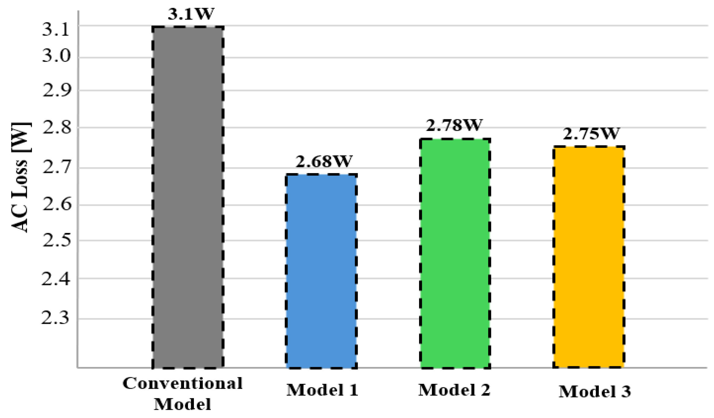
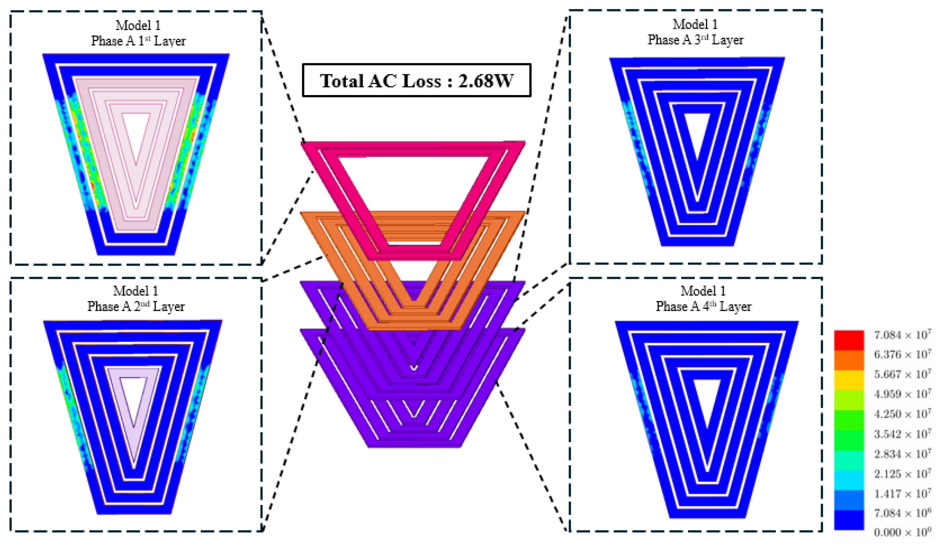
Figure 13 compares the AC losses of the conventional and proposed models, while
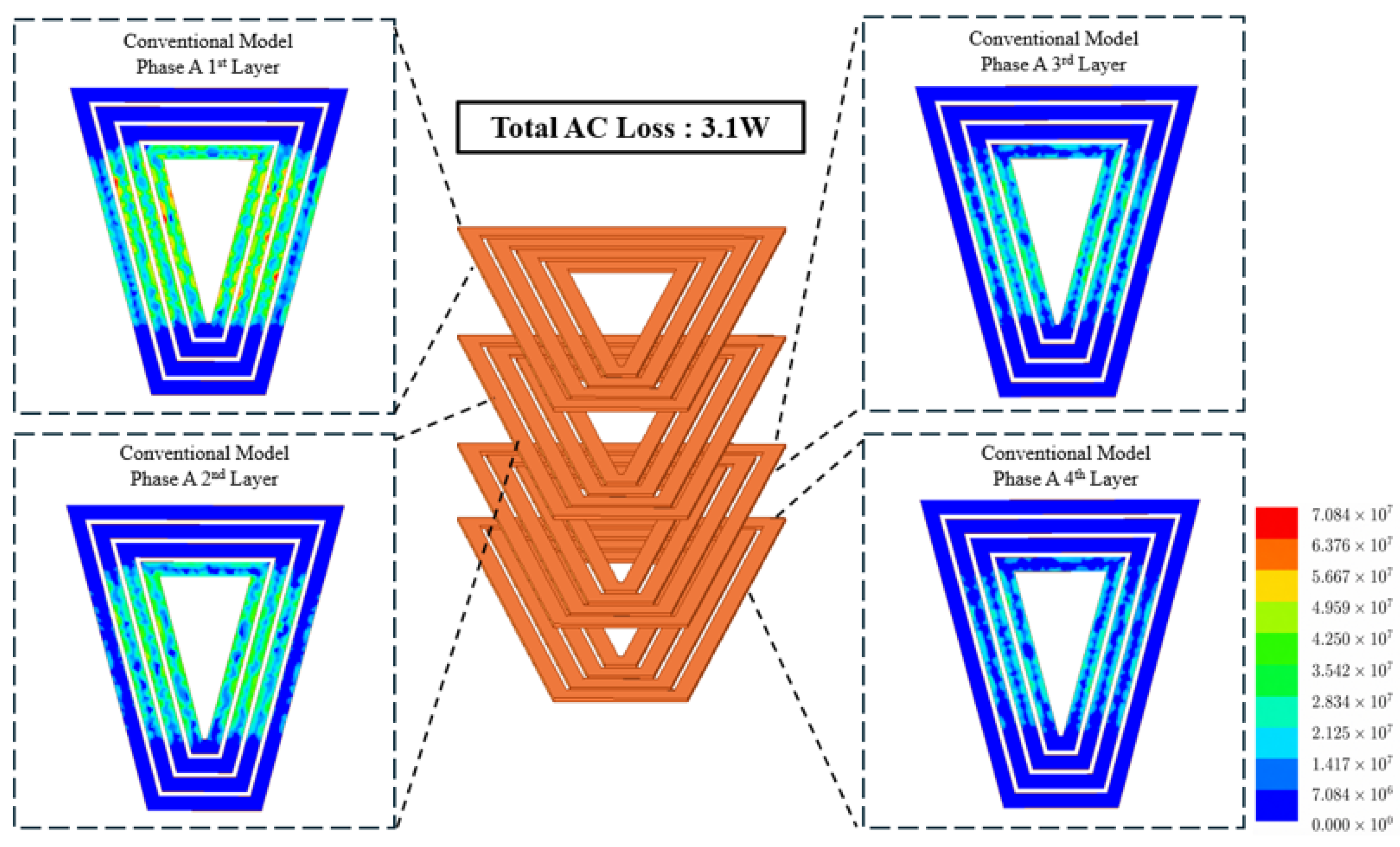
Figure 14 presents the AC loss distribution of Model 1. The AC loss of the conventional model was calculated as 3.10 W, whereas Model 1, Model 2, and Model 3 exhibited AC losses of 2.68 W, 2.78 W, and 2.75 W, respectively. In particular, Model 1 achieved an AC loss reduction of approximately 13.5% compared to the conventional model, showing the best loss performance among the proposed models.
As shown in
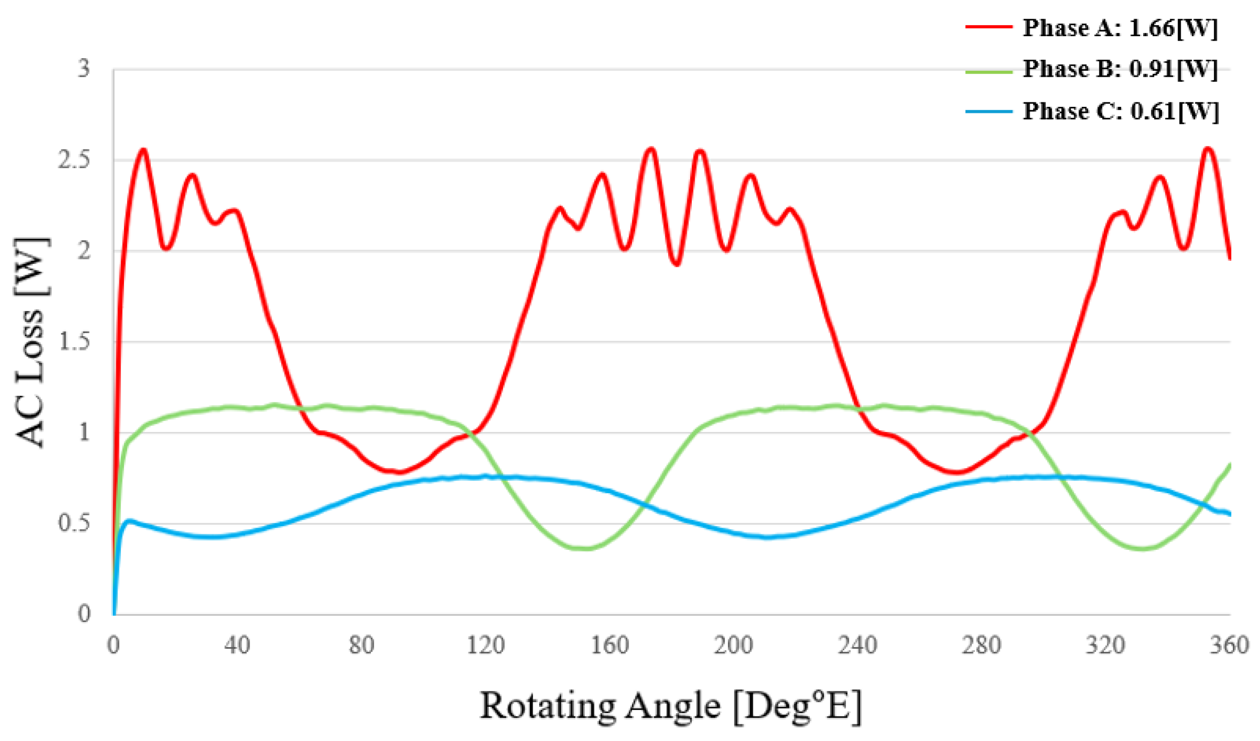
Figure 14, the AC loss concentration observed in the inner-turn regions of the conventional model is significantly alleviated in Model 1. In particular, from the 2nd to the 4th layer, the loss distribution near the inner turns, which was observed in the conventional model, is barely visible. Overall, the AC loss in Model 1 tends to be limited to specific outer conductor regions.
This loss reduction is mainly attributed to the asymmetric turn distribution of Model 1. In the conventional model, all layers of Phase A consist of four turns, meaning that even the inner turns of the upper layers located close to the permanent magnets are directly exposed to the time-varying magnetic flux. In contrast, Model 1 reduces the turn count of the 1st layer of Phase A to two turns and redistributes the turns to lower layers where the magnetic flux influence is relatively weaker. As a result, the effective conductor area directly linked by the strongest magnetic field is reduced.
In addition, the reduction in eddy current components induced in the upper layer also weakens the alternating magnetic field acting on the adjacent layers. Consequently, the AC loss in the inner-turn regions of the 2nd and 3rd layers, which was observed in the conventional model, is reduced. In other words, the loss in the inner turns does not completely disappear; rather, its loss density is reduced to a level that is hardly visible under the same color scale.
Consequently, Model 1 suppresses eddy current generation by reducing the number of turns in high-flux regions close to the permanent magnets and alleviates the proximity effect between adjacent conductors. Therefore, the proposed asymmetric turn distribution is effective not only in mitigating back-EMF imbalance but also in reducing AC loss.
As a result, the proposed asymmetric turn distribution effectively mitigates the back-EMF imbalance while simultaneously reducing AC losses in the concentrated winding PCB AFPM. Unlike the conventional ABCCBA phase arrangement, the proposed method maintains the original AABBCC phase arrangement, thereby avoiding phase resistance imbalance caused by differences in via-hole lengths. Furthermore, by reducing the turn count in high-flux regions close to the permanent magnets and redistributing the turns to regions with relatively lower flux linkage, both back-EMF balance and loss characteristics can be improved simultaneously.
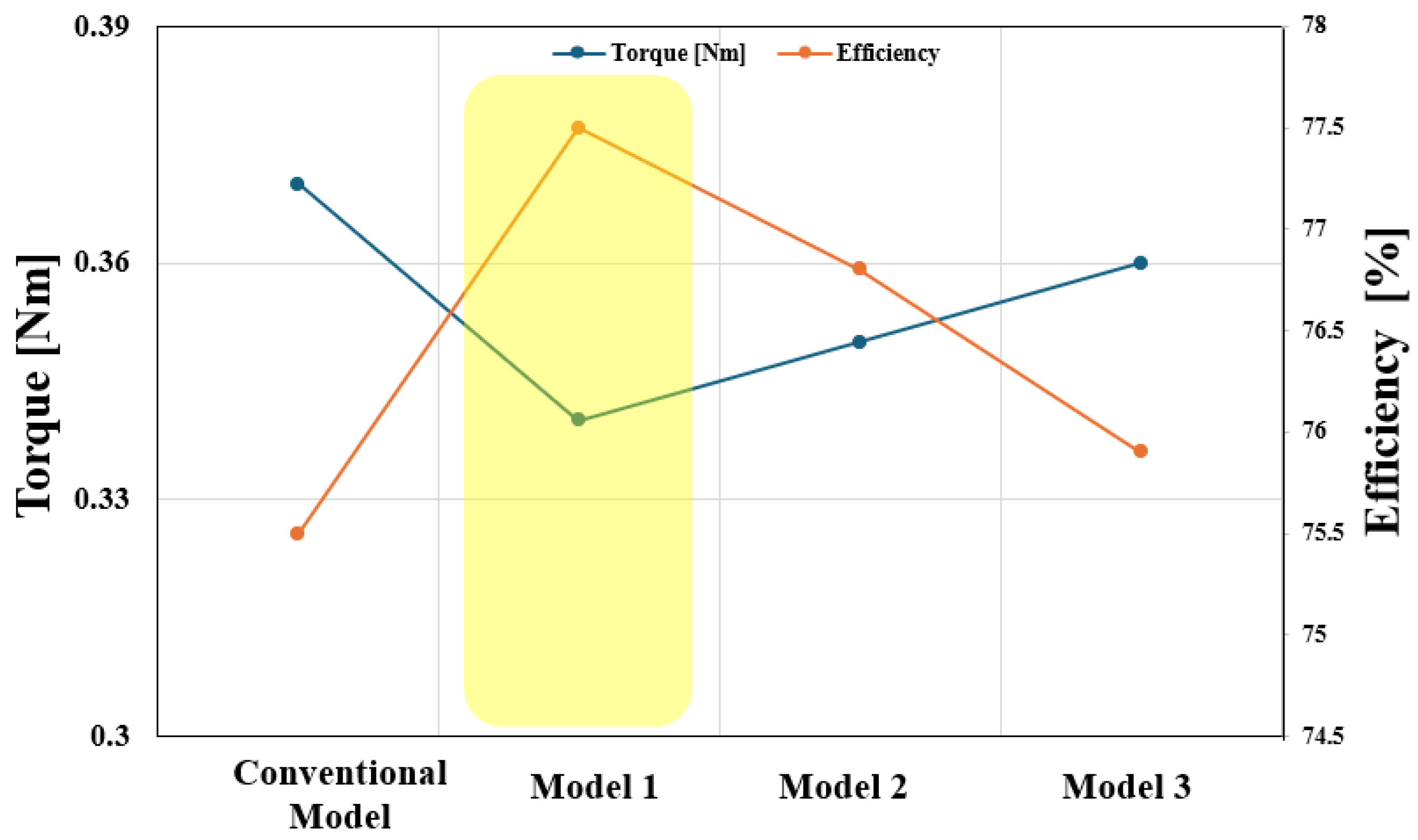
Figure 15 compares the average torque and efficiency of the conventional model and the proposed models. The conventional model exhibits the highest average torque of 0.37 Nm, but its efficiency is limited to 75.5%. In Model 1, the average torque decreases to 0.34 Nm due to the reduced average back-EMF magnitude, whereas the efficiency increases significantly to 77.5%. This indicates that Model 1 provides the most effective efficiency improvement among the proposed models, mainly owing to the reduction in AC loss and the mitigation of phase imbalance.
Model 2 shows an average torque of 0.35 Nm and an efficiency of 76.8%, representing a balanced trade-off between output torque and efficiency. Model 3 exhibits the highest torque among the proposed models, with an average torque of 0.36 Nm, while its efficiency is 75.9%. Although its efficiency improvement is relatively smaller than those of Models 1 and 2, Model 3 maintains the output torque closest to that of the conventional model.
Therefore, the proposed winding arrangements involve a slight torque reduction of 0.01–0.03 Nm compared with the conventional model. However, they improve the phase back-EMF balance and reduce the phase resistance imbalance, thereby enhancing the efficiency and operational stability of the motor. These characteristics are particularly important for compact robotic joint motor applications, where stable and smooth operation is required.
5. Conclusions
This paper investigated the back-EMF imbalance and AC loss characteristics of a single-rotor concentrated winding PCB AFPM for robotic joint applications and proposed an asymmetric turn distribution method to address these issues. Due to the structural characteristics of the concentrated winding PCB pattern, unequal flux linkage among phases results in back-EMF imbalance and increased AC losses.
A conventional ABCCBA phase arrangement was first examined and found to improve back-EMF balance. However, it introduced phase resistance imbalance due to differences in via-hole lengths. To overcome this limitation, an asymmetric turn distribution was applied while maintaining the original AABBCC phase arrangement. By redistributing the turn count according to the axial flux-linkage distribution, phase flux linkage could be compensated without introducing additional phase resistance imbalance.
Finite element analysis results showed that Model 1 achieved the best performance among the proposed models. The back-EMF imbalance ratio was reduced from 39.5% to 8.6%, corresponding to an improvement of approximately 78.2%. In addition, the AC loss was reduced from 3.10 W to 2.68 W, achieving a reduction of approximately 13.5%. The reduction in AC loss was attributed to the decreased eddy-current loss in the layer closest to the permanent magnets and the mitigation of proximity effects in adjacent layers.
Therefore, the proposed asymmetric turn distribution effectively improves both back-EMF balance and AC loss characteristics without causing phase resistance imbalance. The proposed method can be implemented through PCB pattern modification alone and is expected to be an effective design approach for improving the performance of single-rotor PCB AFPMs used in thin-profile robotic joint applications.
Although the proposed method was demonstrated using a 12-layer single-rotor concentrated-winding PCB AFPM, the underlying design principle is not limited to this specific configuration. The proposed approach is based on compensating the layer-dependent flux-linkage variation that inherently exists in multilayer PCB stators. Therefore, the same design concept can be applied to PCB AFPMs with different numbers of PCB layers or different pole/slot combinations, provided that a non-uniform layer-wise flux-linkage distribution exists.
However, this study has several limitations. First, the proposed method was verified only through three-dimensional finite element analysis, and prototype-based experimental validation was not conducted. Second, although AC loss distribution was used as an indirect indicator of potential thermal concentration, detailed electro-thermal coupled analysis was not performed. Third, the applicability of the proposed method to double-rotor PCB AFPM structures was not investigated in this study. Since double-rotor topologies generally exhibit a more symmetric magnetic field distribution across the PCB layers, the effectiveness of the proposed compensation strategy may depend on the magnitude of the layer-wise flux-linkage variation.
Future work will focus on extending the proposed layer-wise turn redistribution strategy to various PCB AFPM configurations, including different layer numbers, slot/pole combinations, and double-rotor structures. In addition, prototype fabrication, back-EMF measurement, phase resistance measurement, torque evaluation, and thermal validation will be conducted to further verify the practical feasibility of the proposed method.