Article

Effect of Cutting Crystal Directions on Micro-Defect Evolution of Single Crystal γ-TiAl Alloy with Molecular Dynamics Simulation

1
School of Mechanical and Electrical Engineering, Lanzhou University of Technology, Lanzhou 730050, China
2
Key Laboratory of Digital Manufacturing Technology and Application, Ministry of Education, Lanzhou University of Technology, Lanzhou 730050, China
3
Centre for Efficiency and Performance Engineering, University of Huddersfield, Huddersfield HD1 3DH, UK
*
Authors to whom correspondence should be addressed.
Metals 2019, 9(12), 1278; https://doi.org/10.3390/met9121278
Submission received: 30 October 2019 / Revised: 23 November 2019 / Accepted: 25 November 2019 / Published: 28 November 2019
(This article belongs to the Special Issue Numerical Modelling and Simulation of Metal Processing)

Abstract

:
In this work, the distribution and evolution of micro-defect in single crystal γ-TiAl alloy during nanometer cutting is studied by means of molecular dynamics simulation. Nanometer cutting is performed along two typical crystal directions: [ 1 ¯ 00 ] and [ 1 ¯ 01 ] . A machined surface, system potential energy, amorphous layer, lattice deformation and the formation mechanism of chip are discussed. The results indicate that the intrinsic stacking fault, dislocation loop and atomic cluster are generated below the machined surface along the cutting crystal directions. In particular, the Stacking Fault Tetrahedron (SFT) is generated inside the workpiece when the cutting crystal direction is along [ 1 ¯ 00 ] . However, a “V”-shape dislocation loop is formed in the workpiece along [ 1 ¯ 01 ] . Furthermore, atomic distribution of the machined surface indicates that the surface quality along [ 1 ¯ 00 ] is better than that along [ 1 ¯ 01 ] . In a certain range, the thickness of the amorphous layer increases gradually with the rise of cutting force during nanometric cutting process.

1. Introduction

With the development of modern industry, nano-processing technology has been widely used in aerospace, biomedical, national defense and military and other high-tech fields [1]. In the fabrication of nanodevices, the basic understanding of the material removal mechanism and the evolution of defects is becoming more and more important. Nanofabrication involves material deformation of only a few atomic layers of about 2–10 nm, and the removal of atoms is discrete and discontinuous. Obviously, experimental and continuous theory is inaccurate. Since the 1990s, Molecular Dynamics (MD) simulation technology has been successfully applied to study the removal mechanism of various materials [2]. The MD can reveal the phenomena that cannot be observed by the traditional method, and capture the structure of material, position and velocity of atoms.
Over past decades, many scholars have done a lot of work by MD method. These studies were mainly focused on monocrystalline silicon, single crystal copper, silicon carbide and monocrystalline nickel that are described by Embedded Atom Method (EAM), Morse and Tersoff potentials. Wang et al. [3] studied the formation mechanism of stress-induced SFT and results show that the complex SFT is nucleated due to tensile and compressive stress. Chuvashia et al. [4] analyzed the mechanism of chip formation under high temperature conditions, and the key conclusion was that less heat is released and larger chips are formed when cutting at higher temperatures or on (111) crystal faces. Besides, the cutting force is reduced by 24% when the temperature at 1173 K compared with room temperature. Xie et al. [5] found that, as cutting-edge radius increases, both the dislocation slip zone and chip formation zone are suppressed while the elastic deformation zone tends to continually grow in monocrystalline copper nano-cutting process by MD simulations. Dai et al. [6] discussed the effects of different tool structures on nanometer cutting of single crystal silicon and found that some structural tools can cause a lower temperature. Fung et al. [7] researched the effect of surface defects of tool on tool wear during nano-machining and the statistical results showed that atoms loss in the defective region of tool is one order of magnitude greater than that in the non-defective region. Ren et al. [8] analyzed the grinding process of monocrystalline nickel at various speeds and depths with the molecular dynamics simulation, and revealed that, owing to the effect of the elastic deformation, a part of the defects can be eliminated after grinding and the dislocations and the variation in the number of HCP atoms cause the change of grinding force. Xu et al. [9] investigated the effect of hard particles on surface generation in nanometer cutting. Liu et al. [10] expounded the evolution of SFT and the work hardening effect in monocrystalline copper. Xu et al. [11] explained the effects of recovery on surface generation in nanometric cutting. Zhu et al. [12] simulated monocrystalline Nickel nano-cutting and found that a stacking fault is main cause of work hardening. Wang et al. [13] found that the tangential and normal forces of the cutting are different in different lattice orientations, and the stacking fault induced by cutting propagates in the basal plane and depends on the angle between the cutting direction and the c-axis through the MD simulations of four off-axis 4H-SiC nano-cutting processes.
The above literature focused on revealing the mechanism of material removal, microdefect evolution, the correlation between chip removal and cutting speed or temperature and cutting force change. However, few studies have focused on the effect of cutting crystal orientation on the evolution of micro-defect in the materials during nano-cutting, and, in particular, the evolution of a micro-defect along different cutting crystal orientation of γ-TiAl alloy has not been found. Additionally, γ-TiAl alloy has the advantage of low density, good high temperature strength and oxidation resistance, so it is widely used in aeroengine and automobile industries [14,15]. γ-TiAl alloy has face-centered tetragonal (FCT) with an L10 structure [16], as shown in Figure 1. Ti atoms and Al atoms are alternately arranged along the [001] direction. Furthermore, the crystal axis ratio of γ-TiAl is c/a = 1.02, which reduces the crystal symmetry and reduces the slip system. Therefore, the mechanical properties are different when cutting in different crystal directions. The purpose of this paper is to research the evolution of micro-defect by cutting along different crystal orientations of γ-TiAl alloy using MD methods. Section 2 will introduce the cutting model and methods. Section 3 will discuss the results of simulation and analyze the evolution of the micro-defect. Finally, the results will be summarized in Section 4.

2. Model and Methods

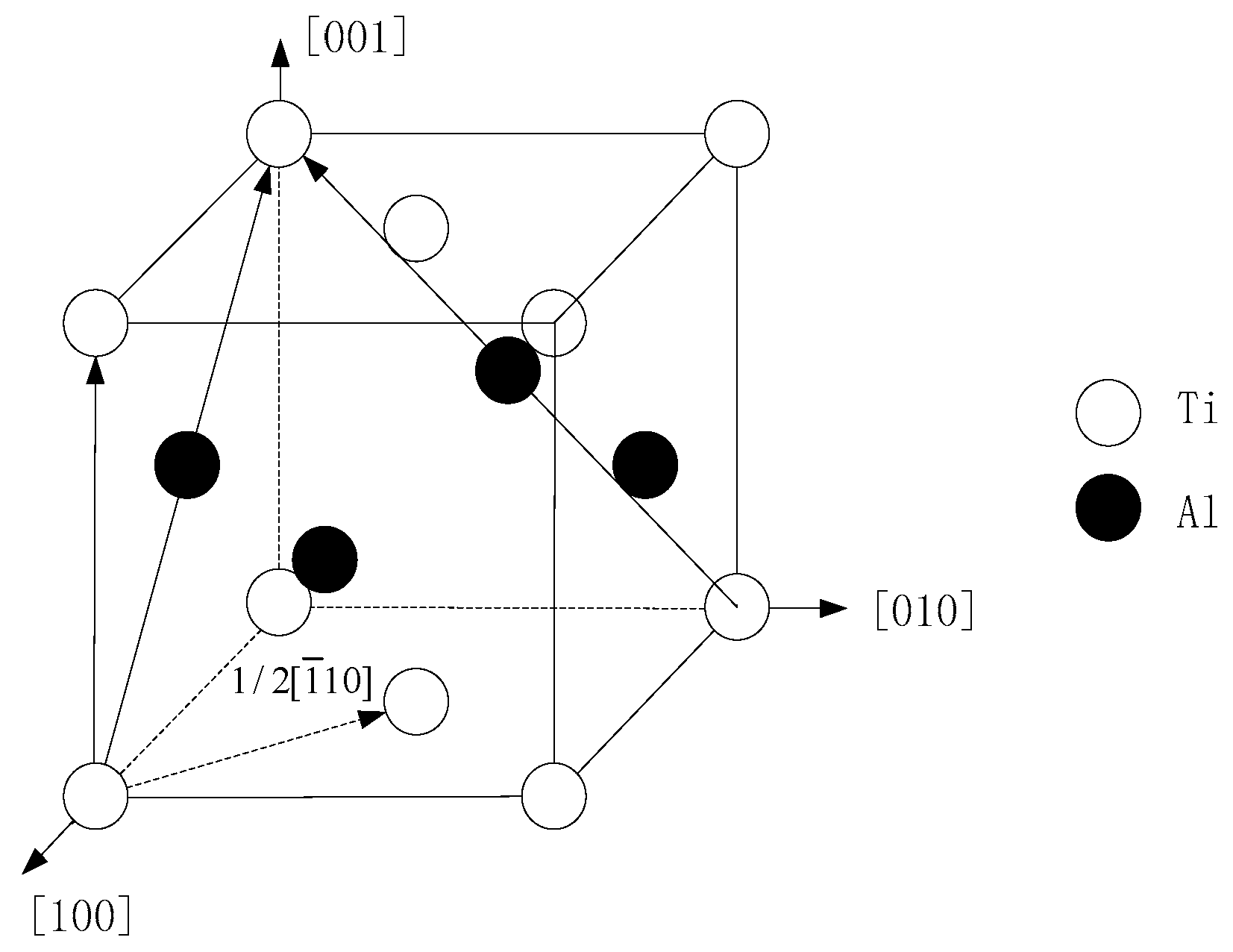
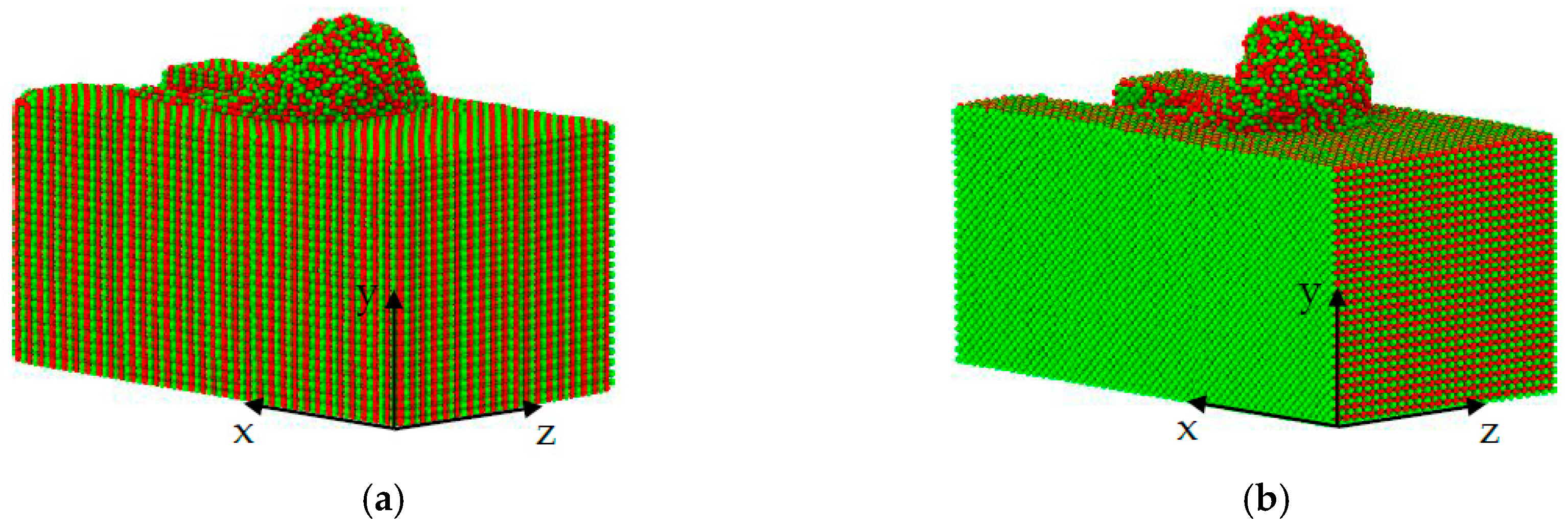
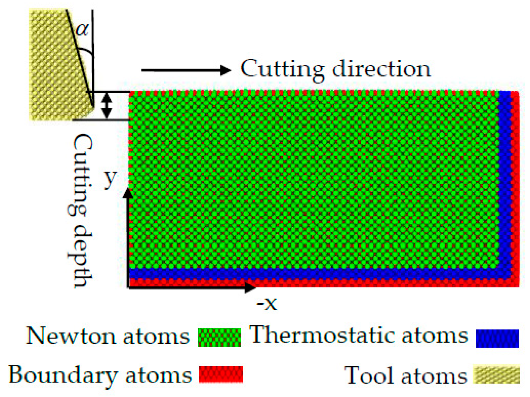
2.1. The MD Simulation Model

As shown in Figure 1, the x, y, and z coordinate axes correspond to the orientations [100], [010] and [001], respectively. The lattice constants are a0 = b0 = 0.4001 nm and c0 = 0.4181 nm, which are consistent with the experimental values a0 = b0 = 0.4005 nm and c0 = 0.40707 nm [17]. The nano-cutting model is shown in Figure 2, consisting of a monocrystalline γ-TiAl workpiece and a diamond tool. The workpiece contains 131,175 atoms and has a size of 20 × 10 × 11 nm3 along the [100], [010] and [001], respectively, and the diamond tool contains 7793 atoms. A periodic boundary condition along the z direction is adopted to eliminate the influence of size effect. In addition, five layers of the right and the bottom edges are fixed, and five layers next to them are a thermostat region which surrounds the Newton atoms. The thermostat region serves as a heat reservoir at a constant temperature 293 K for Newton atoms [18]. Newton atoms are used to study all aspects of the cutting process, the motion of Newton atoms obeys Newton’s second law. Moreover, the selection of cutting speed is based on references [19,20], which combines with the characteristics of the γ-TiAl alloy.

2.2. Interatomic Potential

The reliability of any MD simulation greatly depends on the quality of the interatomic potential employed. For metallic systems, the EAM is a widely used technique [21], which is fitted from a large database of both experiment and abinitio data. The total potential is expressed by
E = i F i ( ρ i ) + 1 2 i j ( i j ) φ i j ( r i j )
ρ i = j ( j i ) f j ( r i j )
where Fi is the embedding energy of atom i, whose electron density is ρi, ϕij is the relative potential energy of atom i and atom j, rij represents the distance between atom i and atom j, Fi(ρi) is the sum of electron cloud density produced by all other atoms, extranuclear electron to atom i, and fj(rij) is the electron density produced by atom j.
The interaction between Al-C and Ti-C is described by Morse potential, and the expression is given by
V ( r i j ) = D e [ e 2 α ( r e r i j ) 2 e α ( r e r i j ) ]
where De is the cohesive energy between atoms i and j, α is the elastic modulus of the material, rij represents the instantaneous distance between atoms i and j, and re is the equilibrium distance between atoms i and j. The parameter of Morse potential can be obtained from Zhu et al. [22]. As DTi-C = 0.982 eV, αTi-C = 22.83 nm−1, rTi-C = 0.1892 nm, DAl-C = 0.28 eV, αAl-C = 27.8 nm−1, rAl-C = 0.22 nm.
As the rigidity of diamond is much higher than that of γ-TiAl, the tool is modeled as a rigid body. Table 1 shows the MD simulation parameters.
In this paper, Common Neighbor Analysis (CNA) [23] is utilized to identify the defect type, such as atomic cluster, dislocation, stacking fault etc.

3. Results and Discussion

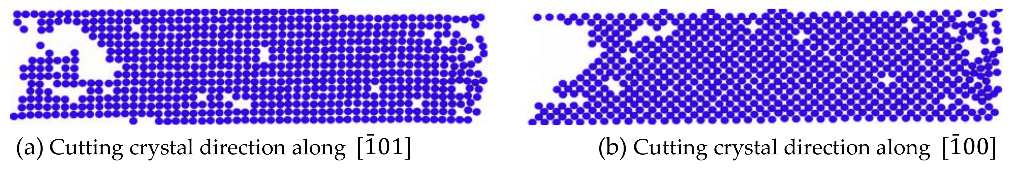
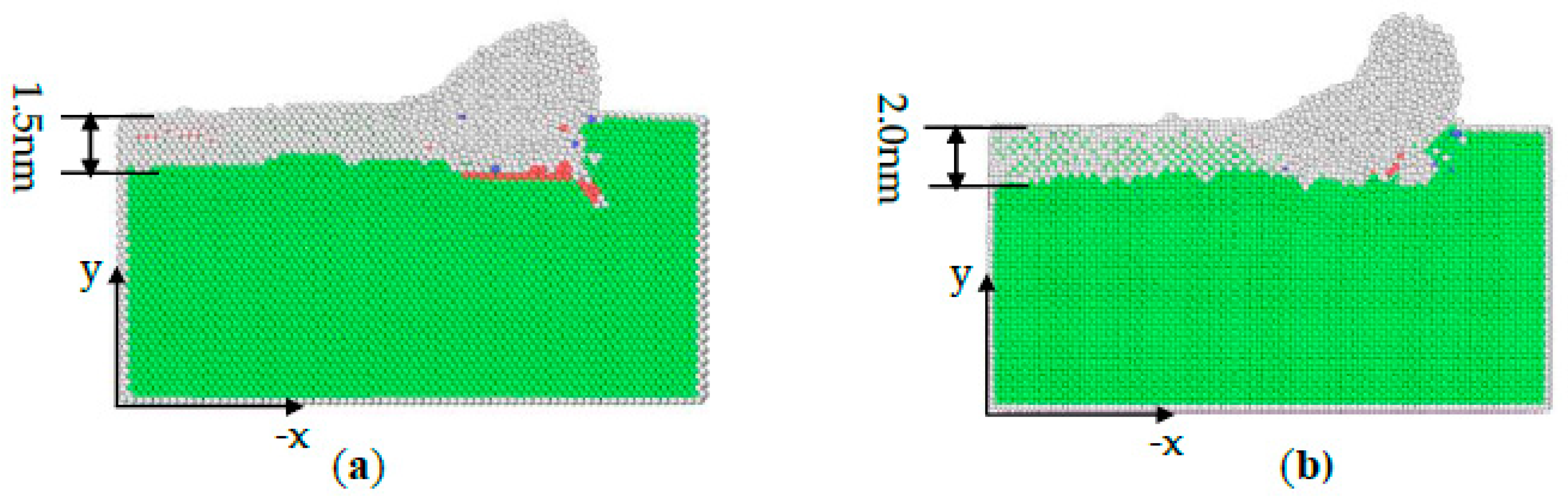
3.1. Material Removal Mechanism in Nanometric Cutting Process

In the nano-cutting process, substrate atoms adjacent to the tool tip are subjected to the high compressive energy, resulting in highly displaced and disordered atoms. Figure 3 shows the diagram of material deformation; (a) and (b) represent the cutting crystal direction along [ 1 ¯ 01 ] and [ 1 ¯ 00 ] , respectively. As shown in Figure 3, in the first place, the lattice orientation is 45° to the tool when the cutting crystal direction is along [ 1 ¯ 01 ] . However, the lattice orientation is 0° or 180° to the tool along [ 1 ¯ 00 ] . In the second instance, the shape of the chip is also different: The chip along [ 1 ¯ 00 ] is higher than that along [ 1 ¯ 01 ] , and the atomic packing is more compact. During the machining process, the elastic and plastic deformation of γ-TiAl occurs with the increase of cutting distance, which is consistent with the literature [24]. The atoms of workpieces are distributed symmetrically on both sides of the tool to form the side-flow, and the others pile up in front of the tool to form chips. The chips are formed by extrusion force from the tool, and is removed in the form of atomic group. Then, the machined surface is generated with a certain elastic recovery.

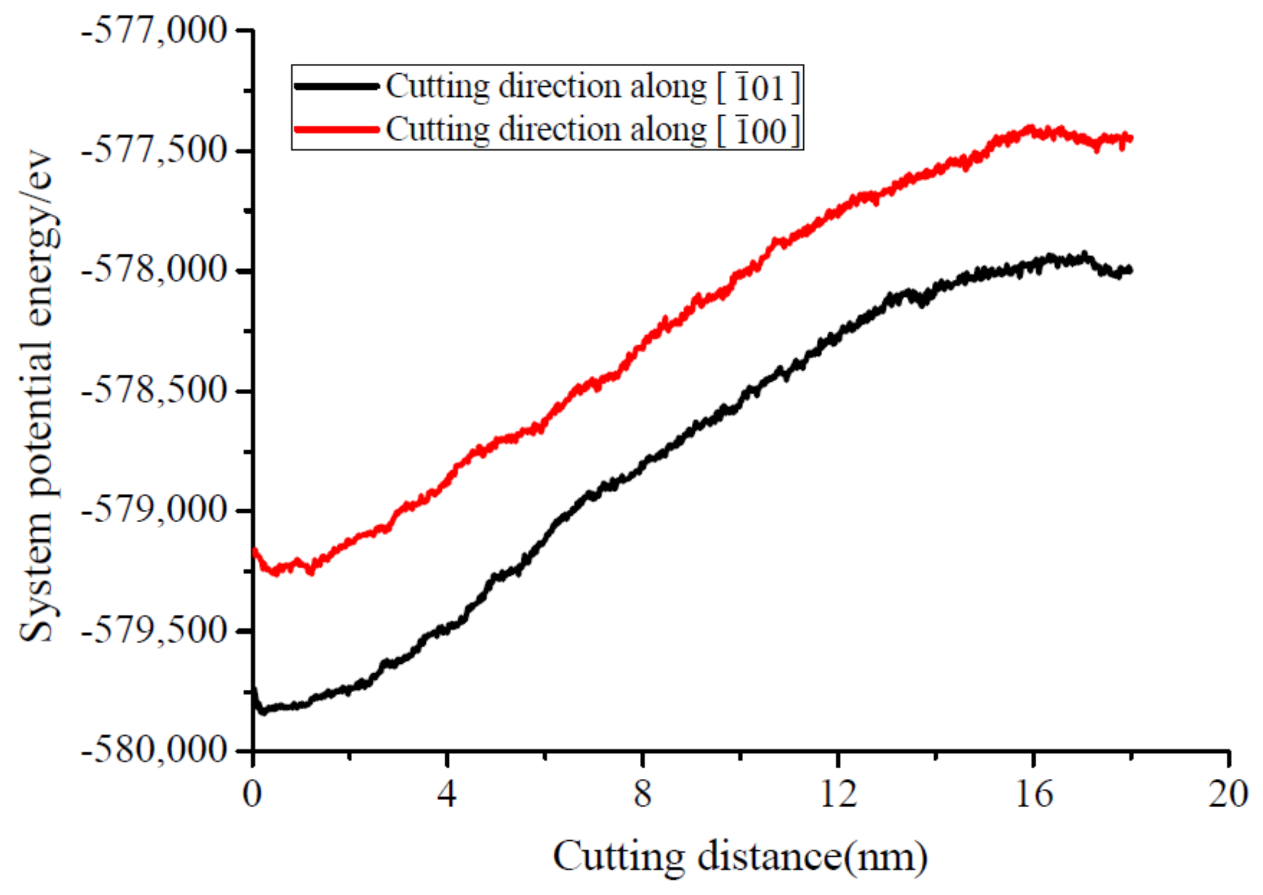
3.2. System Potential Energy and Lattice Deformation in Nanometric Cutting Process

The system potential energy and lattice deformation can be used as indicators of material deformation during the cutting process. Figure 4 shows the effect of different cutting crystal directions on the potential energy of the system, and the two potential energy curves rise with the increase of the cutting distance and the trend of the grows are the same. However, the potential energy of the system is higher than that along [ 1 ¯ 00 ] when the cutting direction is along [ 1 ¯ 01 ] . On one hand, the different lattice arrangements result in different surface energy of the workpiece. On the other hand, the lattice bond breaks more and the internal energy releases more when the cutting direction is along [ 1 ¯ 01 ] . However, the lattice bond breaks less and the internal energy releases less during nanometric cutting along [ 1 ¯ 00 ] .
The CNA method is used to identify the crystal structure transformation during nano-cutting process. Figure 5 shows the effect of cutting directions on atomic structure transition. Figure 5a,b represents the number of structural transitions of HCP (Hexagonal Close-Pack) and BCC (Body-Centered Cubic), respectively. Two bar graphs are compared between the number of HCP transition crystal structure and the number of BCC transition along [ 1 ¯ 01 ] . In the initial stage of cutting, it increases with the increase of cutting distance. The value fluctuates greatly and shows the opposite trend when the cutting distance is 8–16 nm. This is due to the complex stacking faults nucleation, expansion, annihilation. There is a large area of stacking fault at 8–16 nm, which increases the number of HCP transformations and inhibits the number of BCC. The HCP structure plays a dominant role in the whole cutting process. Comparing the number of HCP and BCC transitions along [ 1 ¯ 00 ] , we can see that the BCC crystal structure predominates when the cutting distance is less than 6 nm and more than 14 nm, while the HCP crystal structure dominates and the value fluctuates sharply between 8–14 nm. As the cutting force increases with the increase of cutting distance, which leads to the formation, expansion and annihilation of SFT, thus increasing the number of HCP and decreasing the number of BCC. This indicates that there is a competitive relationship between the transformation of HCP and BCC crystal structures in nano-cutting. It can be seen from Figure 5a that the number of transitions along [ 1 ¯ 01 ] is larger than that along [ 1 ¯ 00 ] , while Figure 5b is just the opposite. As the crystal orientation of the workpiece is 45° with the tool along [ 1 ¯ 01 ] , it is easier to form intrinsic stacking faults; therefore, the number of HCP is greater along [ 1 ¯ 01 ] .

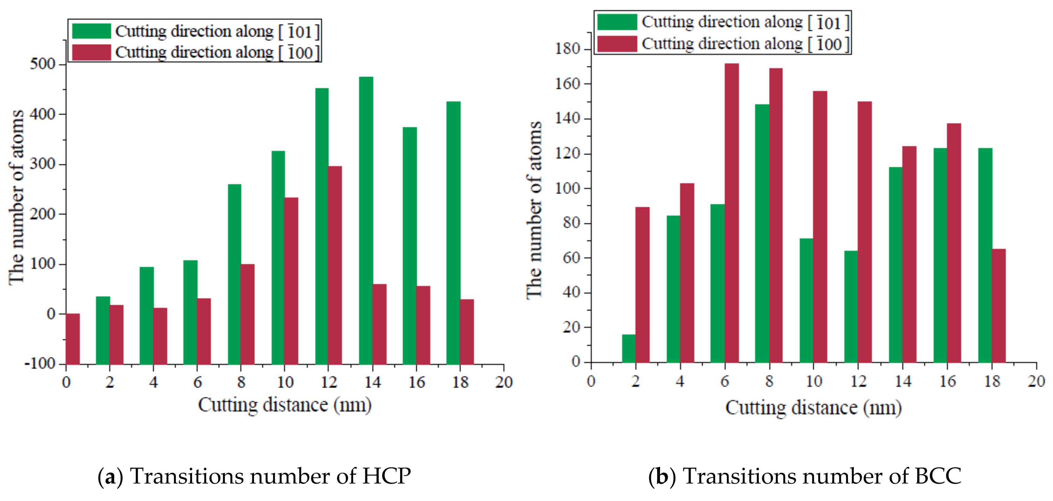
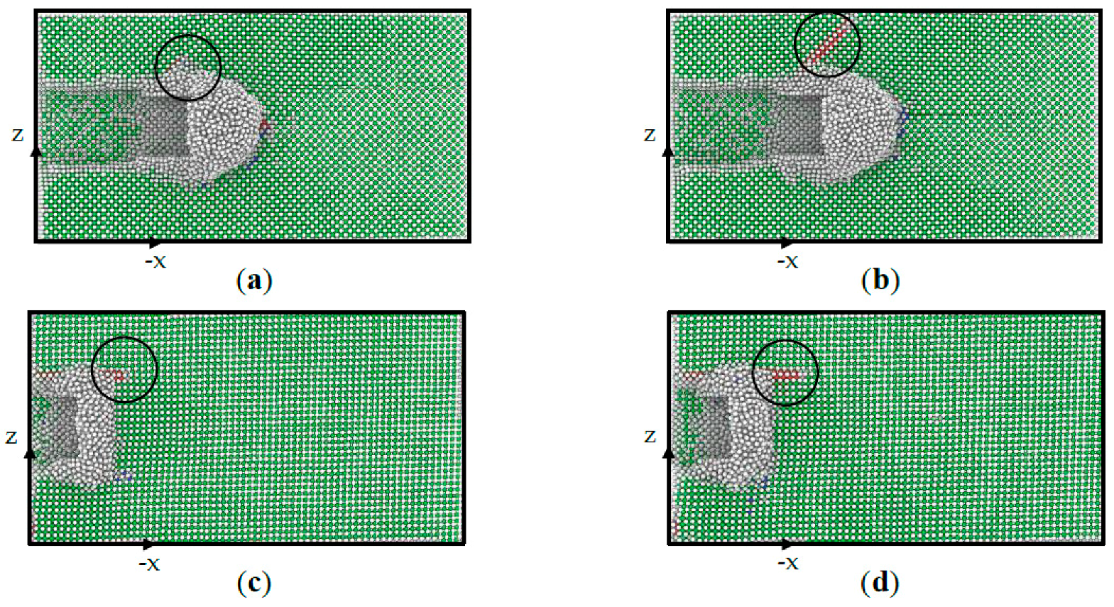
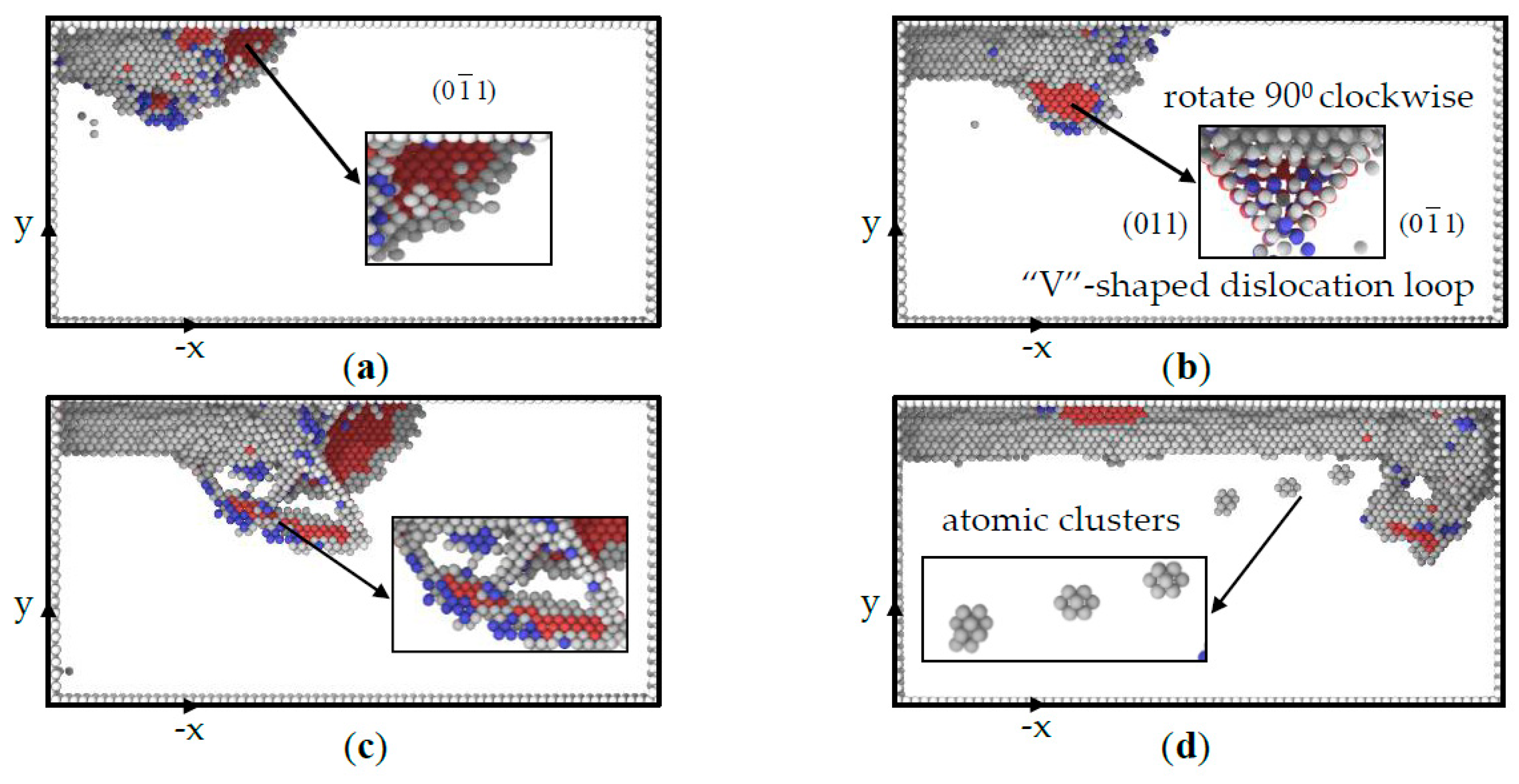
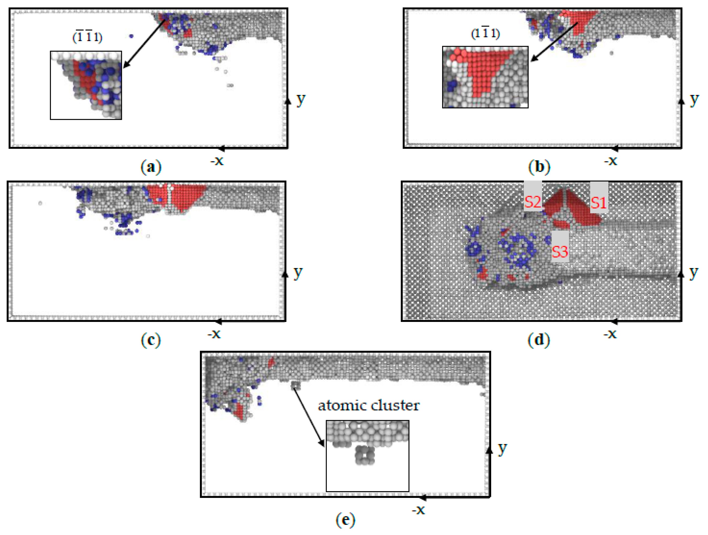
3.3. Evolution of Dislocation in Different Cutting Crystal Direction

In order to clearly understand the evolution process of surface defects during nano-cutting process, Figure 6 shows the effect of different cutting crystal directions on the cutting surface. Figure 6a,b represents dislocation nucleation and dislocation slip along [ 1 ¯ 00 ] and the corresponding time is 124.5 ps and 125.5 ps, respectively. Figure 6c,d represents dislocation nucleation and dislocation slip along [ 1 ¯ 01 ] and the corresponding time is 98 ps and 100 ps, respectively. Among them, white, red and green represent surface atoms (dislocation atoms), HCP atoms and FCC atoms, respectively. The nucleation and slip of dislocations are marked in Figure 6. In the early stage of nano-machining, it can be seen clearly the dislocation nucleated, slide and emitted at 45° to the cutting tool, which is explained by the Schmid rule; the resolved shear stress reaches the maximum value at ±45° in front of the tool and slips in these directions. The dislocation nucleation along [ 1 ¯ 00 ] is late; however, its dislocation slip region is larger than that along [ 1 ¯ 01 ] , as a result of the formation of SFT along [ 1 ¯ 00 ] , which is a reaction between dislocations. Finally, the SFT annihilates to the boundary of the workpiece. Due to the certain image force to dislocation from free surface, the slip area of dislocation increases gradually with the increase of cutting distance, as shown in Figure 6. This is owing to the rise of cutting distance, cutting force and temperature, which contributes to the slip of dislocations during the nanometric cutting process.
The evolution of internal defects in the nanometric cutting process is a dynamic process. Figure 7 shows the internal defects evolution in the workpiece along [ 1 ¯ 01 ] ; atoms are colored according to the CNA. For a better observation of the evolution of defects, ordinary FCC atoms are removed. The white, red and blue represents Other, HCP and BCC atoms, respectively. Two layers of red atom represent an intrinsic stacking fault [25]. In the early stage of the nano-machining, the stacking fault is generated along ( 0 1 ¯ 1 ) crystal planes for the instability of the cutting, as shown in Figure 7a. The stacking fault nucleates and extends at shear-slip zone below the cutting tool, and finally annihilates at free surface of workpiece, as depicted in Figure 7b. Two Shockley partial dislocations extend along ( 011 ) and ( 0 1 ¯ 1 ) planes and form a Lomer-Cottrell lock [26], which finally forms a “V”-shaped dislocation loop, as illustrated in Figure 7b. In the middle stage of nanomachining, it can be seen clearly that the complex dislocation loop and the stacking fault are generated beneath the tool attributing to the rise of cutting force and temperature, as shown in Figure 7c. With the increase of cutting distance, the stacking fault and the complex dislocation loop disappear gradually and are removed in the form of chips, as depicted in Figure 7d. However, the defects continue to evolve in the workpiece, and a small number of the atomic clusters are generated inside the workpiece, as illustrated in Figure 7d. The atomic clusters are formed as a result of the combined effects of temperature and plastic deformation during nano-cutting.
Figure 8 shows the internal defect evolution inside the workpiece along [ 1 ¯ 00 ] . It can be seen that the stacking fault, the SFT, the dislocation loop and the atomic cluster are formed in the subsurface. The stacking fault in the shear-slip zone extends along the ( 1 ¯ 1 ¯ 1 ) and ( 1 1 ¯ 1 ) planes, as shown in Figure 8a,b. After processing, there are two stacking faults slipping along each slip direction, which finally annihilate at free surface of the workpiece. As can be seen from Figure 8c,d, the complex SFT consists of three edges, three stacking fault planes and one workpiece surface, which are formed in the subsurface of the workpiece. The order of the nucleation of the intrinsic stacking fault is marked “S1”, “S2”, “S3”, where 1/3<001> Hirth dislocation is formed between “S1” and “S2”, 1/6<112> Shockley partial dislocation is produced between “S2” and “S3”, and 1/6<110> Stair-rod dislocation is generated between “S1” and “S3” along the respective slip surfaces, in which Stair-rod and Hirth are immobile dislocations to preserve the shape of the SFT. As a result of the instability of external forces during the cutting process, the SFT is eventually removed in the form of chips, and a small number of atomic clusters and dislocation loops are formed, as illustrated in Figure 8e.

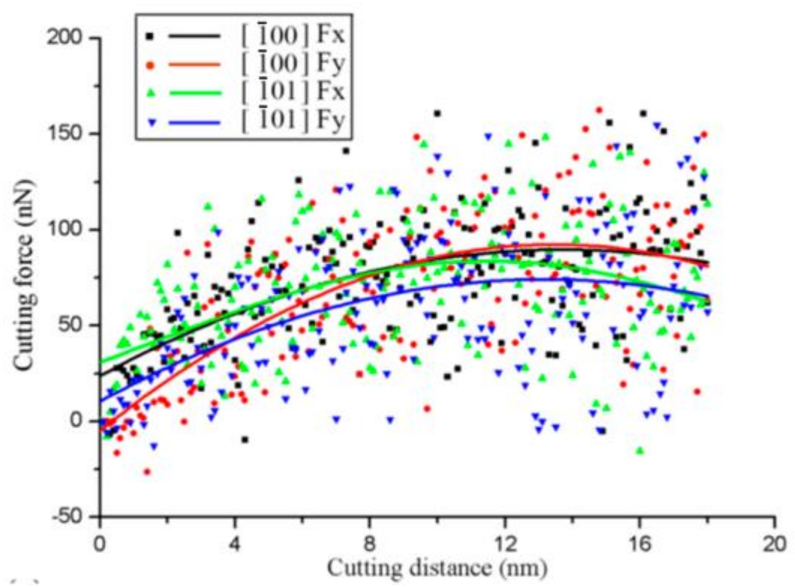
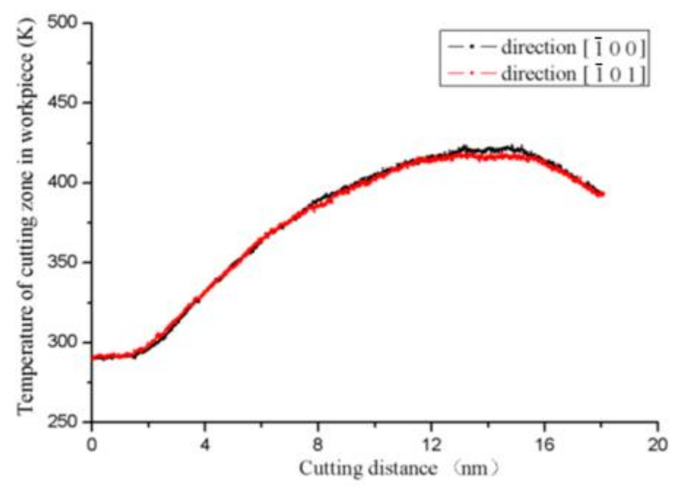
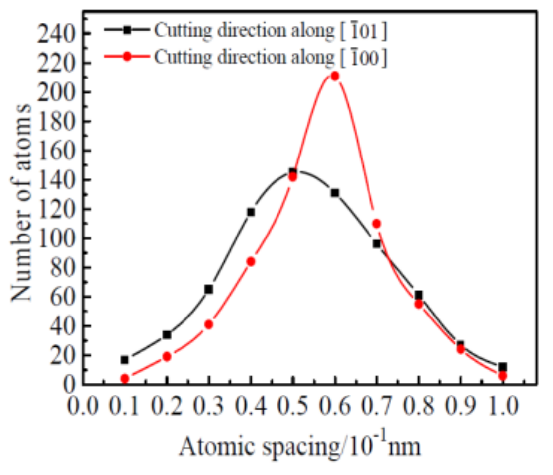
3.4. Effect of Cutting Crystal Direction on Cutting Force, Temperature and Cutting Surface Quality

The cutting force is an indispensable factor in the analysis of the nanometer cutting process. Figure 9 shows tangential force, Fx and Fy, in the cases with different cutting crystal directions. It is noticeable that when the tool and the workpiece are close to a certain distance, the workpiece atoms give a certain repulsive force to the tool, where the cutting force has a negative value. Subsequently, the Fx increases rapidly with cutting distance and becomes gradually stable. This conforms with reference [27]. The tangential force is basically stable and fluctuates within a certain range when the cutting distance exceeds 6 nm, and the fluctuation of the curve is caused by crystal structure transformation, stacking fault and lattice reconstruction. In addition, there is a consistent trend in the curve of Fx for the cutting crystal directions. In Figure 10, the temperature of the cutting zone grows along with increase of cutting distance before the distance reaches 15 nm. Comparing derivation of the temperature and the cutting force, the temperature of the workpiece grows along with the increase of cutting force at the early stage of cutting. During the final of the cutting process, the temperature goes down, which happens as the cutting force drops. The temperature of workpiece with cutting direction of [ 1 ¯ 00 ] is higher when the cutting distance is between 12 nm and 16 nm than that of the one along the [ 1 ¯ 01 ] direction. This phenomenon results in the resistance of materials varying along different directions and more heat being generated during the cutting of a workpiece along the [ 1 ¯ 00 ] direction.
In order to clearly distinguish the size of the cutting force, this article details statistics of the average cutting force. Besides, the cutting distance is selected between 6–18 nm, which aims to reduce error of the cutting force. The average cutting force is shown in Table 2. It can be clearly seen that the average cutting force along [ 1 ¯ 00 ] is greater than that along [ 1 ¯ 01 ] . This results from the interaction of dislocations along [ 1 ¯ 00 ] , which activates more dislocation slip systems and intersects in the cutting direction, and, in consequence, the greater cutting force is required for material removal than that along [ 1 ¯ 01 ] . This is in line with reference [28]. When the cutting crystal direction changes from [ 1 ¯ 01 ] to [ 1 ¯ 00 ] , the tangential force and normal force is increased by 13.32%, 10.25%, respectively.
The quality of the cutting surface is crucial during nanometer cutting process. Figure 11 shows the atomic distribution of machined surface under different cutting crystals. Figure 11a,b represents the cutting direction along [ 1 ¯ 01 ] and along [ 1 ¯ 00 ] , respectively. The blank area in the figure means the atom lost in cutting, and there is a large atom loss area. The number of atoms remaining on the machined surfaces in Figure 11a,b is 706 and 697, respectively, and these two numbers are close. In order to analyze the surface quality more accurately, the y-direction distribution of atoms on the top layer of the machined surface is calculated. As shown in Figure 11, the black and red curves represent the y-direction distribution of atoms along [ 1 ¯ 01 ] and [ 1 ¯ 00 ] , respectively. It can be seen that the atom distribution span along [ 1 ¯ 01 ] is 0.01–0.1 nm, with the largest number of atoms at 0.05 nm, and its peak value is 145. However, the atom distribution span along [ 1 ¯ 00 ] is 0.01–0.1 nm, and the peak value is 211 at 0.06 nm. From the analysis of data and curve distribution, it can be seen that the atomic spans of the two cutting directions are the same. Furthermore, the y-direction atom distribution along [ 1 ¯ 00 ] is more concentrated and compact, which shows that the machined surface quality along [ 1 ¯ 00 ] is better than that along [ 1 ¯ 01 ] .
In order to analyze the effect of different cutting directions on the quality of the cutting surface, the atomic distribution in the First layer along the y-direction was quantified, that is, the unevenness of the First layer atomic plane. Figure 12 shows the effect of different cutting directions on atomic distribution. It can be seen that both curves have multiple peaks; the maximum number of atoms is 135, 87 at 0.15 nm, 0.145 nm. Secondly, the distribution of atoms along [ 1 ¯ 00 ] is concentrated, while the distribution of atoms along [ 1 ¯ 01 ] is dispersed. This indicates that the distance between atoms is smaller and the planeness is better than that along [ 1 ¯ 01 ] . When the cutting direction is along [ 1 ¯ 01 ] , the orientation of the lattice is 45° to the tool, resulting in smaller fluctuations of atoms in the nano-cutting process.
As shown in Figure 13, the effect of different cutting directions on the amorphous layer is displayed. The amorphous layer is composed of dislocation and disordered atoms, which is formed below the machined surface. Figure 13a,b represents the cutting direction along [ 1 ¯ 01 ] and [ 1 ¯ 00 ] , respectively. It is clear that the thickness of amorphous layer along [ 1 ¯ 00 ] is slightly larger than that along [ 1 ¯ 01 ] . The cutting force along [ 1 ¯ 00 ] is slightly higher than that along [ 1 ¯ 01 ] . This, in a certain range, the deeper the thickness of the amorphous layer, the greater the cutting force during the nanometric cutting process.

4. Conclusions

In this paper, the nanometric cutting process of single crystal γ-TiAl alloy has been studied by molecular dynamics simulation. The effect of cutting directions on the material deformation, system potential energy, lattice deformation, machined surface, cutting force and the evolution of dislocation are thoroughly discussed. The conclusions are as follows:
(1) The orientation of the lattice is 45° to the tool when the cutting crystal direction is along [ 1 ¯ 01 ] . However, the arrangement of the lattice is 0° or 180° to the tool when the cutting direction is along [ 1 ¯ 00 ] , and the chips are removed as atomic groups. The potential energy of cutting orientation along [ 1 ¯ 01 ] is larger than that along [ 1 ¯ 00 ] .
(2) The evolution of defects is affected by cutting directions in the workpiece. Dislocation slip starts at the cutting surface. Inside the workpiece, the intrinsic stacking faults, dislocation loops and atomic clusters are generated. The SFT is produced inside the workpiece when the cutting direction is along [ 1 ¯ 00 ] . However, a “V”-shape dislocation loop is generated when the cutting direction is along [ 1 ¯ 01 ] .
(3) As the cutting direction changes from [ 1 ¯ 01 ] to [ 1 ¯ 00 ] , the tangential force and normal force is increased by 13.32% and 10.25%, respectively. Quantitative analysis of atomic distribution along the y-direction proves that the machined surface quality along [ 1 ¯ 00 ] is better than that along [ 1 ¯ 01 ] . The thickness of the amorphous layer along [ 1 ¯ 00 ] is slightly deeper than that along [ 1 ¯ 01 ] .

Author Contributions

Conceptualization, R.F.; methodology, R.F. and J.L.; software, J.L.; formal analysis, H.Q.; investigation, H.Q. and Y.Q.; resources, H.L.; data curation, H.L. and M.W.; writing—original draft preparation, H.Q.; writing—review and editing, R.F. and J.L.; visualization, H.Q. and J.L.; supervision, R.F. and C.L.

Funding

This research was funded by a grant from the China Scholarship Council, grant number 201808625035, the National Natural Science Foundation of China, grant number 51865027; the Program for Changjiang Scholars and Innovative Research Team in University of Ministry of Education of China, grant number IRT_15R30; and the Hongliu First-class Disciplines Development Program of Lanzhou University of Technology.

Acknowledgments

The technical support of Gansu Province Supercomputer Centre is gratefully acknowledged.

Conflicts of Interest

The authors declare no conflict of interest.

References

  1. Gong, Y.D.; Zhu, Z.X.; Zhou, Y.G.; Sun, Y. Research on the nanometric machining of a single crystal nickel via molecular dynamics simulation. Sci. Chin. Technol. Sci. 2016, 59, 1–10. [Google Scholar] [CrossRef]
  2. Guo, Y.B.; Liang, Y.C. Atomistic simulation of thermal effects and defect structures during nanomachining of copper. Trans. Nonferrous Met. Soc. China 2012, 22, 2762–2770. [Google Scholar] [CrossRef]
  3. Wang, Q.L.; Bai, Q.S.; Chen, J.X.; Guo, Y.B.; Xie, W.K. Stress-induced formation mechanism of stacking fault tetrahedra in nano-cutting of single crystal copper. Appl. Surf. Sci. 2015, 355, 1153–1160. [Google Scholar] [CrossRef]
  4. Chuvashia, S.Z.; Luo, X. An atomistic simulation investigation on chip related phenomena in nanometric cutting of single crystal silicon at elevated temperatures. Comput. Mater. Sci. 2016, 113, 1–10. [Google Scholar] [CrossRef]
  5. Xie, W.K.; Fang, F.Z. Effect of tool edge radius on material removal mechanism in atomic and close-to-atomic scale cutting. Appl. Surf. Sci. 2019, 144451. [Google Scholar] [CrossRef]
  6. Dai, H.F.; Chen, G.Y.; Zhou, C.; Fang, Q.H.; Fei, X.J. A numerical study of ultraprecision machining of monocrystalline silicon with laser nano-structured diamond tools by atomistic simulation. Appl. Surf. Sci. 2017, 393, 405–416. [Google Scholar] [CrossRef]
  7. Fung, K.Y.; Tang, C.Y.; Cheung, C.F. Molecular dynamics analysis of the effect of surface flaws of diamond tools on tool wear in nanometric cutting. Comput. Mater. Sci. 2017, 133, 60–70. [Google Scholar] [CrossRef]
  8. Ren, J.; Hao, M.R.; Lv, M.; Wang, S.Y.; Zhu, B.Y. Molecular dynamics research on ultra-high-speed grinding mechanism of monocrystalline nickel. Appl. Surf. Sci. 2018, 455, 629–634. [Google Scholar] [CrossRef]
  9. Xu, F.; Fang, F.; Zhang, X. Hard particle effect on surface generation in nano-cutting. Appl. Surf. Sci. 2017, 425, 1020–1027. [Google Scholar] [CrossRef]
  10. Liu, H.T.; Zhu, X.F.; Sun, Y.Z.; Xie, W.K. Evolution of stacking fault tetrahedral and work hardening effect in copper single crystals. Appl. Surf. Sci. 2017, 422, 413–419. [Google Scholar] [CrossRef]
  11. Xu, F.; Fang, F.; Zhang, X. Effects of recovery and side flow on surface generation in nano-cutting of single crystal silicon. Comput. Mater. Sci. 2018, 143, 133–142. [Google Scholar] [CrossRef]
  12. Zhu, Z.X.; Gong, Y.D.; Zhou, Y.G.; Gao, Q. Molecular dynamics simulation of single crystal Nickel nanometric machining. Sci. China Technol. Sci. 2016, 59, 867–875. [Google Scholar] [CrossRef]
  13. Wang, M.; Zhu, F.; Xu, Y.; Liu, S. Investigation of Nanocutting Characteristics of Off-Axis 4H-SiC Substrate by Molecular Dynamics. Appl. Sci. 2018, 8, 2380. [Google Scholar] [CrossRef]
  14. Appel, F.; Clemens, H.; Fischer, F.D. Modeling concepts for intermetallic titanium aluminides. Prog. Mater Sci. 2016, 81, 55–124. [Google Scholar] [CrossRef]
  15. Schwaighofer, E.; Rashkova, B.; Clemens, H.; Stark, A.; Mayer, S. Effect of carbon addition on solidification behavior, phase evolution and creep properties of an intermetallic β-stabilized γ-TiAl based alloy. Intermetallics 2014, 46, 173–184. [Google Scholar] [CrossRef]
  16. Chubb, S.R.; Papaconstantopoulos, D.A.; Klein, B.M. First-principles study of L10 Ti-Al and V-Al alloys. Phys. Rev. B 1988, 38, 120–124. [Google Scholar] [CrossRef]
  17. Tang, F.L.; Cai, H.M.; Bao, H.W.; Xue, H.T.; Lu, W.J.; Zhu, L.; Rui, Z.Y. Molecular dynamics simulations of void growth in γ-TiAl single crystal. Comput. Mater. Sci. 2014, 84, 232–237. [Google Scholar] [CrossRef]
  18. Romero, P.A.; Anciaux, G.; Molinari, A.; Molinar, J.F. Insights into the thermo-mechanics of orthogonal nanometric machining. Comput. Mater. Sci. 2013, 72, 116–126. [Google Scholar] [CrossRef]
  19. Liu, Y.; Li, B.; Kong, L. A molecular dynamics investigation into nanoscale scratching mechanism of polycrystalline silicon carbide. Comput. Mater. Sci. 2018, 148, 76–86. [Google Scholar] [CrossRef]
  20. Wang, J.; Zhang, X.; Fang, F. Molecular dynamics study on nanometric cutting of ion implanted silicon. Comput. Mater. Sci. 2016, 117, 240–250. [Google Scholar] [CrossRef]
  21. Daw, M.S.; Baskes, M.I. Embedded-atom method: Derivation and application to impurities, surfaces, and other defects in metals. Phys. Rev. B 1984, 29, 6443–6453. [Google Scholar] [CrossRef]
  22. Zhu, Y.; Zhang, Y.; Qi, S.; Xiang, Z. Titanium Nanometric Cutting Process Based on Molecular Dynamics. Rare Met. Mater. Eng. 2016, 45, 897–900. [Google Scholar] [CrossRef]
  23. Faken, D.; Jónsson, H. Systematic analysis of local atomic structure combined with 3D computer graphics. Comput. Mater. Sci. 1994, 2, 279–286. [Google Scholar] [CrossRef]
  24. Zhu, P.; Fang, F. On the mechanism of material removal in nanometric cutting of metallic glass. Appl. Phys. A 2014, 116, 605–610. [Google Scholar] [CrossRef]
  25. Swygenhoven, H.V.; Derlet, P.M.; Frøseth, A.G. Stacking fault energies and slip in nanocrystalline metals. Nat. Mater. 2004, 3, 399–403. [Google Scholar] [CrossRef]
  26. Liang, Y.C.; Wang, Q.L.; Yu, N.; Chen, J.X.; Zha, F.S.; Sun, Y.Z. Study of Dislocation Nucleation Mechanism in Nanoindentation Process. Nanosci. Nanotechnol. Lett. 2013, 5, 536–541. [Google Scholar] [CrossRef]
  27. Sharma, A.; Datta, D.; Balasubramaniam, R. An investig- ation of tool and hard particle interaction in nanoscale cutting of copper beryllium. Comput. Mater. Sci. 2018, 145, 208–223. [Google Scholar] [CrossRef]
  28. Dai, H.; Chen, G. A molecular dynamics investigation into the mechanisms of material removal and subsurface damage of nanoscale high speed laser-assisted machining. Mol. Simul. 2017, 43, 42–51. [Google Scholar] [CrossRef]
Figure 1. L10 structure of γ-TiAl.
Metals 09 01278 g001
Figure 2. The MD simulation model of nano-cutting.
Metals 09 01278 g002
Figure 3. The diagram of cutting distances at 12 nm and the cutting crystal directions along [ 1 ¯ 01 ] , [ 1 ¯ 00 ] respectively, (green represents Ti and red represents Al). (a) Cutting crystal direction along [ 1 ¯ 01 ] . (b) Cutting crystal direction along [ 1 ¯ 00 ] .
Metals 09 01278 g003
Figure 4. Change curve of system potential energy in the nanometric cutting process.
Metals 09 01278 g004
Figure 5. Graph of atomic structure variations with the cutting distance on the surface.
Metals 09 01278 g005
Figure 6. Variation of cutting surface in nanometric cutting process. (a) Dislocation nucleation at 124.5 ps along [ 1 ¯ 00 ] . (b) Dislocation slip at 125.5 ps along [ 1 ¯ 00 ] . (c) Dislocation nucleation at 98 ps along [ 1 ¯ 01 ] . (d) Dislocation slip at 100 ps along [ 1 ¯ 01 ] .
Metals 09 01278 g006
Figure 7. Internal defect evolution of workpiece along [ 1 ¯ 01 ] . (a) Stacking fault along ( 0 1 ¯ 1 ) . (b) “V”-shaped dislocation loop. (c) Dislocation loop and stacking fault. (d) Atomic clusters.
Metals 09 01278 g007
Figure 8. Internal defect evolution of the workpiece along [ 1 ¯ 00 ] . (a) Stacking fault along ( 1 ¯ 1 ¯ 1 ) . (b) Stacking fault along ( 1 1 ¯ 1 ) . (c) SFT. (d) Nucleation of the intrinsic stacking fault. (e) Atomic clusters.
Metals 09 01278 g008
Figure 9. Tangential force.
Metals 09 01278 g009
Figure 10. Temperature of cutting zone.
Metals 09 01278 g010
Figure 11. Atomic distribution of machined surface under different cutting crystals.
Metals 09 01278 g011
Figure 12. Y-direction atom distribution in the top layer of machined surface under different cutting crystals.
Metals 09 01278 g012
Figure 13. Effect of cutting direction on thickness of amorphous layer. (a) Thickness of amorphous layer along [ 1 ¯ 01 ] . (b) Thickness of amorphous layer along [ 1 ¯ 00 ] .
Metals 09 01278 g013
Table 1. The MD simulation parameters.
Machining ParametersValue
Potential functionEAM, Morse
WorkpieceSingle crystal γ-TiAl
ToolDiamond
Workpiece size20 × 10 × 11 nm3
Lattice structureL10
Tool rake angle α15°
Tool clearance angle β
Tool edge radius R1.5 nm
Cutting speed200 m/s
Cutting depth1.5 nm
Cutting direction < 100 > [ 1 ¯ 00 ] , < 110 > [ 1 ¯ 01 ]
Timestep1fs
Table 2. Cutting force for the two simulation cases.
Average Stress Type Cutting Crystal Directions
[ 1 ¯ 01 ] [ 1 ¯ 00 ]
ave Fx (nN)81.76392.655
ave Fy (nN)79.39187.531

