Review

Impurity Effects in Electroplated-Copper Solder Joints

1
Department of Chemical Engineering, National Chung Hsing University, Taichung 402, Taiwan
2
Innovation and Development Center of Sustainable Agriculture (IDCSA), National Chung Hsing University, Taichung 402, Taiwan
*
Author to whom correspondence should be addressed.
Metals 2018, 8(6), 388; https://doi.org/10.3390/met8060388
Submission received: 24 April 2018 / Revised: 17 May 2018 / Accepted: 25 May 2018 / Published: 28 May 2018

Abstract

:
Copper (Cu) electroplating is a mature technology, and has been extensively applied in microelectronic industry. With the development of advanced microelectronic packaging, Cu electroplating encounters new challenges for atomic deposition on a non-planar substrate and to deliver good throwing power and uniform deposit properties in a high-aspect-ratio trench. The use of organic additives plays an important role in modulating the atomic deposition to achieve successful metallic coverage and filling, which strongly relies on the adsorptive and chemical interactions among additives on the surface of growing film. However, the adsorptive characteristic of organic additives inevitably results in an incorporation of additive-derived impurities in the electroplated Cu film. The incorporation of high-level impurities originating from the use of polyethylene glycol (PEG) and chlorine ions significantly affects the microstructural evolution of the electroplated Cu film, and the electroplated-Cu solder joints, leading to the formation of undesired voids at the joint interface. However, the addition of bis(3-sulfopropyl) disulfide (SPS) with a critical concentration suppresses the impurity incorporation and the void formation. In this article, relevant studies were reviewed, and the focus was placed on the effects of additive formula and plating parameters on the impurity incorporation in the electroplated Cu film, and the void formation in the solder joints.

1. Introduction

Copper (Cu) has been receiving considerable attention in the microelectronic industry due to its superior electrical and thermal conductivity as a good conducting material. In board level applications, such as in printed circuit boards (PCBs), Cu is the primary material used to fabricate the circuits. In chip level development, Damascene Cu interconnect technique [1] has gradually replaced traditional aluminum (Al) to improve electromigration (EM) resistance, so as to sustain high-level current impact in advanced microelectronics. The trends of portability, wearability, and multifunctionality have also pushed the microelectronic industry to develop ultrafine pitch and high-density interconnections, in which through-silicon-via (TSV) [2,3] is a promising technique to reach the goal. In TSV technology, Cu is used to fill the via as an interconnect. There are several matured techniques that can fabricate the Cu wire/interconnect, such as sputtering, evaporation, and electrochemical deposition, among which electrochemical deposition (also known as electroplating) is a cost-effective method capable of making uniform and hole-filling Cu metallization [1,4,5,6]. In addition to basic constitutes such as sulfuric acid and copper sulphate, it is necessary to add several functional additives in the plating bath to assist or modulate the deposition of Cu atoms on non-planar substrates [7,8,9,10,11,12,13,14]. For example, in TSV Cu-filling process, two typical organic additives are usually used, one is polyethylene glycol (PEG) and the other is bis(3-sulfopropyl) disulfide (SPS). PEG is a kind of suppressor, and Cl ions from sodium chloride (NaCl) or hydrogen chloride (HCl) are necessary to add in the plating bath to co-work with PEG. PEG and Cl ions chelate with the Cu ions in the plating solution to form a PEG–Cu+–Cl complex on the Cu deposit. This chelation reaction tends to occur on the planar regions outside the via, forming a molecular complex layer on the Cu deposit which acts as a diffusion barrier to block the movement of Cu ions and suppress the deposition rate of Cu [7,8,9]. On the contrary, SPS is a common accelerator with a higher diffusion rate which can enhance the deposition rate of Cu inside the via to accomplish superfilling by a bottom-up mechanism [10]. The acceleration process of SPS is assisted by adsorbing on the Cu deposit using its head adsorbing group (disulfide) and attracting the Cu ions using its terminal anion group (sulfonic acid) [11,12,13].
The use of functional additives plays a key role in the electrodeposition of Cu on non-planar substrate. However, these additives have strong adhesion on the surface of the Cu deposit [7,8,15], and are inevitably incorporated into the Cu deposit during electrodeposition [16,17,18]. The incorporation of organic additives in the Cu deposit has been identified to cause some severe reliability problems. For example, the existence of impurity originated from the incorporation of organic additives suppresses the grain boundary movement due to the Zener pinning effect [19]. When the impurities in the form of second-phase inclusions or particles, such as very small oxides and sulfides, locate in a grain boundary, the interaction between grain boundary and second-phase inclusion produces a drag force which hinders the grain boundary motion [20]. As a result, the grain growth is suppressed, which fails to reduce the circuit resistivity by means of post-annealing. Besides, the impurity residues can also cause pinhole problem on the Cu deposit [21].
Sn-containing solder alloy is a joining material that is used to join the Cu metallizations to form solder joints as an electrical path in the microelectronic products. The joining is accomplished by a liquid/solid (solder/Cu) reaction performed at a temperature higher than the melting point of solder. The Sn-Cu intermetallic compounds (IMCs), Cu6Sn5 and Cu3Sn, usually form in the solder joint during the joining reaction, and continue to grow in the subsequent storage and operation period [22,23]. The formation of IMCs at the joint interface ensures the success of joining, but their growth may accompany the formation of Kirkendall voids caused by an imbalance of atomic fluxes between Sn and Cu [24,25]. Normally, Cu diffuses at a faster rate than Sn in the Cu3Sn phase, so vacancies generate and oversaturate to form Kirkendall voids in the Cu3Sn phase [24,25]. In general, the growth of Kirkendall voids exhibit a strong dependence on the growth of the Cu3Sn phase, that is, the thicker the Cu3Sn phase, the more the voids. Therefore, it is feasible to suppress the growth of Kirkendall voids by suppressing the Cu3Sn growth. Doping of minor element (Pd, Fe, or Ni) in the solder alloy has been shown to be an effective method to suppress the Cu3Sn growth, and therefore, the growth of Kirkendall voids [26,27]. In addition to Kirkendall void, the impurity incorporation in the Cu deposit also causes the formation of voids in the electroplated-Cu solder joints [16,17,18,28,29,30,31,32]. Compared with the Kirkendall effect, the impurity effect is more complicated and pronounced on the growth of voids in the solder joint. Voids are formed massively at the Cu3Sn/Cu interface and inside the IMC layers [18,30,31], not specifically inside the Cu3Sn phase, as with the Kirkendall voids. Additive formula, aging of plating solution, and plating current density are all influential in the incorporation level of impurities in the electroplated Cu films and voiding behavior in the solder joints. Since the formation of voids is detrimental to the mechanical and electrical performance, such an impurity effect appears to be an important reliability concern in the electroplated-Cu solder joints.
Although the addition level of organic additives in the Cu-plating solution is low, the strong adhesion characteristic of the additives causes a non-negligible incorporation level of impurity in the Cu deposit, and a significant effect on the void formation and IMC growth in the solder/Cu joints [16,17,18,29,30,31,33,34,35]. Following the development trend of fine and even ultrafine pith for three-dimensional integrated-circuit (3D IC) packaging, the geometry of the solder joint becomes more complicated, i.e., the aspect ratio of a TSV will increase. The dimension of the solder joint will also shrink. It is expected that the functional additives play a more and more important role in the electrodeposition of Cu, and therefore, the impurity effect becomes more and more significant. The void formation will also become a more fatal reliability problem in a fine and advanced ultrafine solder joint [36]. Therefore, it is necessary to have a comprehensive understanding of the impurity effect, and thereby, to propose a solution that can effectively suppress the impurity incorporation in the Cu deposit. In this review article, most of the related papers were reviewed, and they were divided into the following two main sections: electroplating of Cu, and effects of impurity on interfacial reaction of Sn/Cu solder joint. In the first section, functional additives used for the electrodeposition of Cu were introduced, and their incorporation in the Cu deposit was discussed. In the second section, the impurity effect on the void formation and IMC growth was discussed.

2. Electroplating of Cu

Electroplating has been an important technology for metallic deposition since its first development by an Italian chemist, Luigi Brugnatelli, in 1805. The first electroplating factory was then built in Birmingham, England, in 1840, and the main purpose of electroplating was decoration. A historical development of electroplating technology is its application in microelectronic industry in the 1950s and 1960s. Plated through hole (PTH) technology was developed to electrically connect both sides of a PCB for multilayer application. Besides, electroplated Cu foil is widely used in copper clad laminate (CCL) as the printed-circuit material. Development of high density interconnection (HDI), Damascene Cu interconnect, and TSV are other milestones of electroplating technology. New and specific plating formulas were developed to assist the Cu deposition inside a micro-via. During the via filling process, the organic additives play a crucial role in precisely controlling the deposition rate of Cu inside and outside the via. Basically, the deposition rate of Cu on the surface and side wall of the via is suppressed, while that on the bottom of the via is accelerated. Therefore, the via filling process can be accomplished through a bottom-up mechanism (super filling). It needs to be mentioned that the via filling with reduced voids and seams can also be achieved by increasing the electrolyte movements into via, specifically using megasonic-assisted plating [37]. However, the review focus is mainly placed on the effects of organic additives here.

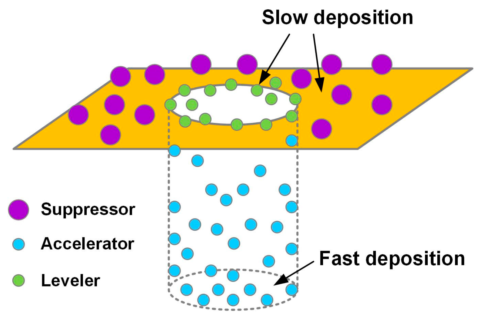
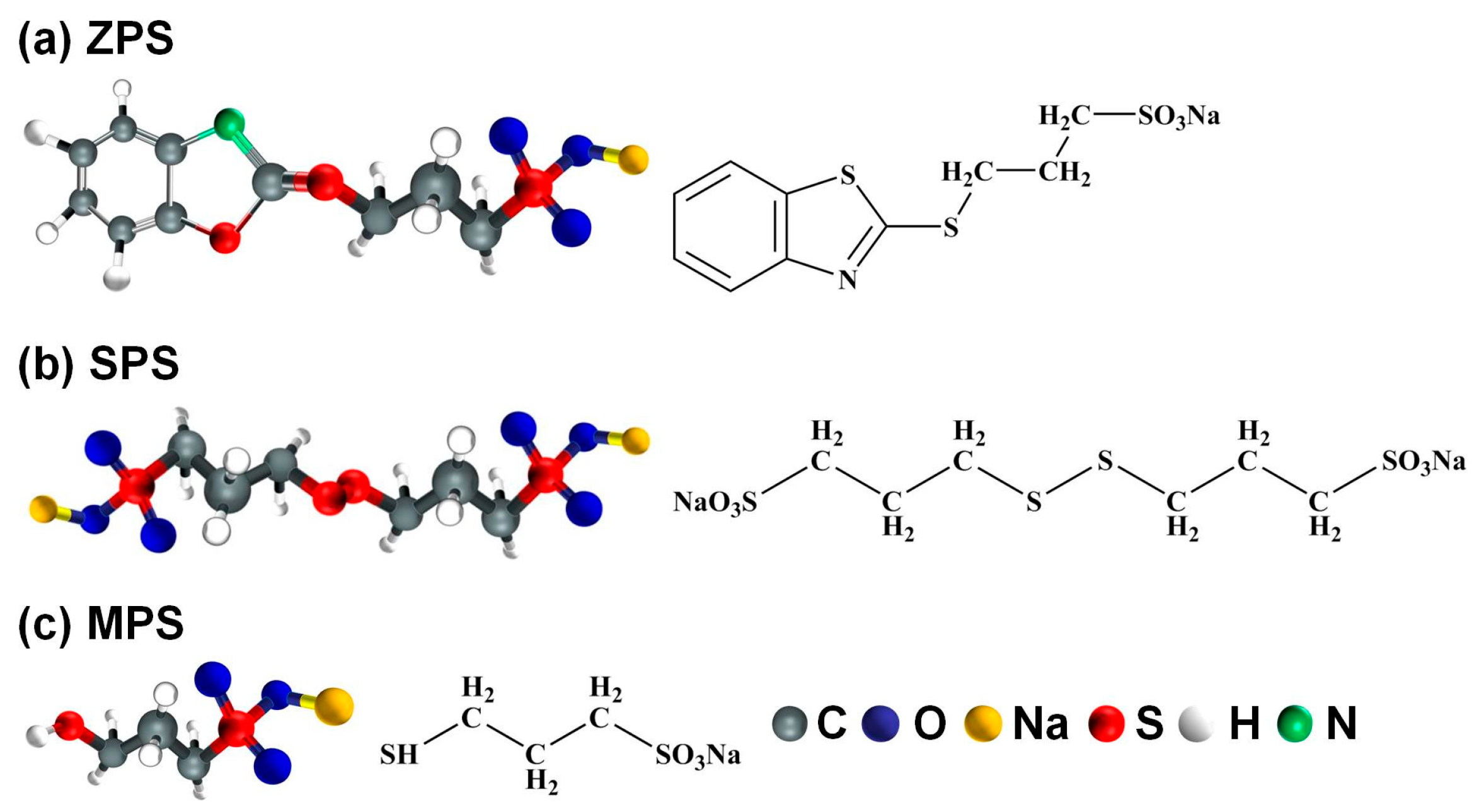
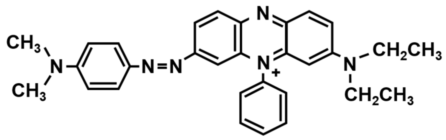
2.1. Functional Additives Used for Electrodeposition of Cu

A typical formula of a Cu-plating solution contains a basic electrolyte and several additives. The constituents of a basic electrolyte are usually Cu sulfate and sulfuric acid, in which Cu sulfate is the main source of the Cu ions, and sulfuric acid controls the pH value to adjust the electrolyte conductivity. Table 1 lists the concentrations of the two primary constituents suggested for various applications [38]. The use of additives is to modulate the current density distribution on the surface of plated substrate, and thereby control the deposition rate of Cu. The common additives include suppressor, accelerator, and leveler. If we take a blind hole as an example for the electrodeposition of Cu, the working mechanisms of the additives inside and outside the blind hole are schematically shown in Figure 1. The suppressor adsorbs on the surface of the substrate (outside the hole), which blocks the diffusion of Cu ions and suppresses the deposition rate of reduced Cu atoms on the surface. The accelerator molecules can enter into the hole and adsorb on the bottom of the hole to accelerate the deposition rate of Cu. The periphery of the hole entrance attracts greater electrical field lines, and thus, locally increases the currents. Due to the positively charged characteristic, the leveler molecules tend to adsorb at the periphery of the hole entrance, where the current concentrates, which can suppress the deposition rate of Cu on the hole entrance to avoid void formation inside the hole due to fast sealing of the hole entrance [39,40,41]. Besides, NaCl or HCl is usually added in the plating solution to offer chlorine ions to assist in adhesion of additive molecules on the plated substrate [8]. The concentration of additives is usually as low as tens or hundreds of ppm; however, an appropriate formula or combination of the functional additives can generate a synergistic effect capable of perfectly filling the hole without voids or seams.

2.1.1. Suppressor

Suppressor is usually a high-molecular-weight polymer bearing a molecular structure of ethylene or propylene glycol, such as polyethylene glycol (PEG) or polypropylene glycol (PPG). In the electroplating process, the suppressor needs to work synergistically with Cl ions to have a chelation reaction with the cuprous ions (Cu+), so as to suppress the deposition rate of Cu. In 1998, Kelly et al. [8,15] studied the interaction between PEG and Cl ions and their polarization behavior on the cathode surface using linear sweep voltammetry (LSV), quartz crystal microbalance (QCM), and electrochemical impedance spectroscopy (EIS). They found that PEG molecules displayed a column-shaped morphology, as the plating solution was free of Cl ions. However, a spherical shape was detected for PEG molecules in the presence of Cl ions. The Cu ions were encapsulated in the spheres by forming a PEG–Cu+–Cl complex, and therefore, the deposition rate of Cu was suppressed. In other words, a higher overpotential was needed for reduction reaction of the Cu atoms on the deposit surface. In 2003, Feng et al. proposed a possible configuration of the PEG–Cu+–Cl complex based on the results of surface-enhanced Raman spectra [7]. As shown in Figure 2, each Cu+ ion has three coordination bonds with two oxygen atoms and one Cl ion to form the PEG–Cu+–Cl complex, where the Cl ion is adsorbed on the cathode surface due to its specific adsorption ability on the cathode surface [42]. Moffat et al. suggested that the complex worked as a passivating film on the deposit surface, which regulated the deposition rate of Cu by making it two orders of magnitude slower [43]. The suppression of deposition rate is also likely due to competition for active sites on the depositing surface by adsorptive PEG molecules [44]. In 2005, Dow et al. [6] studied the influence of the molecular weight of PEG, and found that the higher the molecular weight of PEG, the stronger the suppression effect on the deposition rate of Cu.

2.1.2. Accelerator

Bis(3-sulfopropyl) disulfide (SPS), 3-mercapto-1-propanesulfonate (MPS), and 3-(2-benzthiazolylthio)-1-propanesulfonsäure (ZPS) are common accelerators. As shown in Figure 3, the typical molecular structure of accelerator contains a terminal anion group (sulfonic acid) for attracting the Cu ions in the electrolyte and a head sulfur-containing group capable of adsorbing on the Cu deposit. The adsorptive head group toward the metallic surface is HS, –S–S–, and –C–S–C– for MPS, SPS, and ZPS, respectively. Dow et al. [6] studied the influence of SPS by post-addition of SPS in the plating bath originally containing PEG and Cl ions. They found that the overpotential decreased with the addition of SPS, showing that SPS has strong competitive adsorption strength capable of replacing the adsorption sites of PEG. Choe et al. [45] studied the degradation behavior of SPS using H-type nuclear magnetic resonance (H-NMR). The results showed that SPS oxidized to 3-mercapto-1-propane sulfonic acid (MPSA) and 1,3-propane disulfonic acid (PDS) in the electroplating process, in which MPSA was able to reconvert to SPS but PDS was not. Therefore, degradation of SPS was attributed to the irreversible transformation from SPS to PDS. Since degradation of SPS causes loss of SPS, which is unfavorable for acceleration, replenishment of SPS is an important step to maintain the electroplating quality in the electroplating process. According to the overpotential analysis, Dow et al. [46] found that the acceleration performance of three accelerators is in the following order: MPS > 3-S-thiuronium propanesulfonate (UPS) > ZPS. Therefore, the use of ZPS required a higher concentration (20 ppm) so as to have hole-filling performance comparable to low-level MPS (1 ppm). This big concentration difference is attributed to the fact that ZPS is a weak accelerator, because its benzothiazolyl head group acts as a geometrical barrier and hinders effective adsorption on the Cu surface. As a result, it needs to add a high level of ZPS to reduce the overpotential, and thereby improves its acceleration effect.

2.1.3. Leveler

Leveler is an azole compound containing nitrogen atoms. Figure 4 shows the molecular structure of a commercial leveler, JGB (Janus Green B) [39]. Due to the positively charged amine (or nitro) group, the leveler prefers to “automatically” adsorb on the region where the current concentrates. By contrast, the suppressor, i.e., PEG, needs to co-work with Cl ions in a forced convection environment to enable its adsorption on the deposition surface. In the via filling process, leveler primarily adsorbs on the via opening, and works as a suppressor to inhibit the deposition rate of Cu around the via opening. The local suppression of Cu deposition can avoid the formation of void or seam inside the via.

2.2. Impurity Residues in Electroplated Cu Layer

The grain size in an as-plated Cu layer is usually sub-micron to a few microns. To lower the total interfacial energy, grain growth occurs at room temperature, which is termed as self-annealing. Such a self-annealing phenomenon has been identified by in situ observation [47,48,49,50], and the resultant grain growth can reduce the electrical resistivity [51] and enhance the anti-electromigration performance [52] of the electroplated Cu layer. However, the use of additives may cause a high level of impurity incorporation in the as-plated Cu layer, and inhibit self-annealing of Cu due to Zener pinning effect. The existence of impurity in the as-plated Cu layer is also harmful to the electrical conductivity.

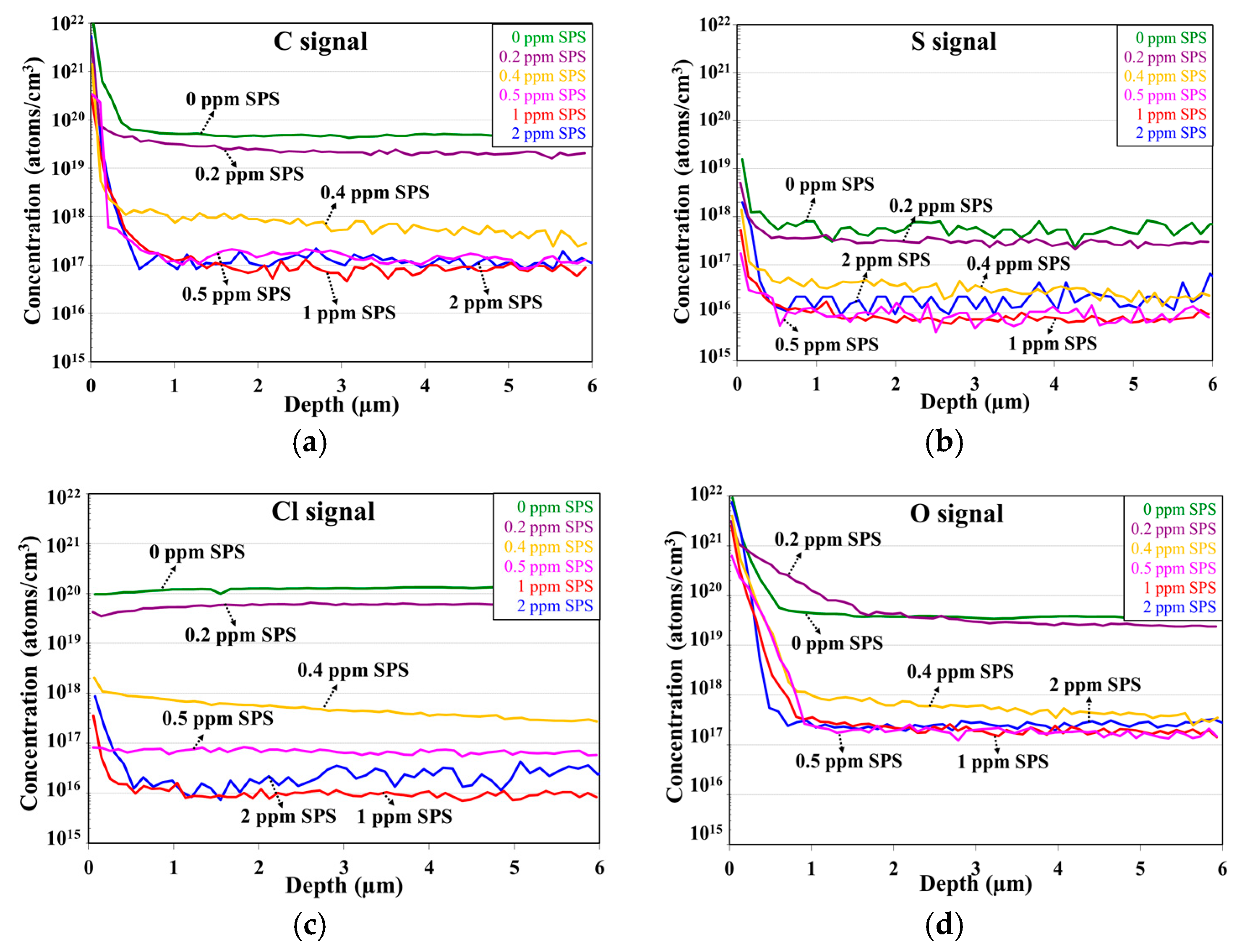
2.2.1. Effects of Plating Parameter and Additive Formula on Impurity Incorporation

Stangl et al. [19] studied the aging effect on the plating solution and its influences on the electrical resistivity and microstructure of the Cu-plated layer. Due to decomposition of SPS in the aged solution, the as-plated Cu layer displayed a smaller grain size and an increased surface roughness. By adding new SPS in the plating solution, the grain size became bigger, and surface roughness decreased. The evolution of the electrical resistivity in the storage process also showed strong aging dependence. When the plating solution was fresh, a reduction of 20% in the electrical resistivity of the Cu-plated layer was observed after a 5 h storage. However, the same reduction of the electrical resistivity needed a longer storage time of 15 h for an aged plating solution. This slower reduction of the electrical resistivity is likely due to the incorporation of impurity (sulfur and carbon) in the Cu-plated layer fabricated using the aged solution. The authors also compared the impurity content in the two Cu-plated layers fabricated by direct and pulse current plating using secondary ion mass spectrometer (SIMS). Based on the qualitative analysis, both 1000 nm-thick Cu-plated layers showed much higher intensities for some impurities (chlorine and sulfur) at the bottom, as compared with other regions throughout the film, indicating that the adsorptive additive molecules concentrated on the surface of the plating substrate and were incorporated in the growing layer during the deposition of Cu atoms. Besides, the Cu-plated layer made by pulse current had a higher level of impurity content which was attributed to an effective supplement of additives onto the deposit surface in the off interval. Cheng et al. [51] found that the impurity level increased with increasing the current density, no matter whether the plating mode was direct or pulse. However, their results showed that direct plating resulted in a higher impurity content which was opposite to that of Stangl et al. [19].
Researchers at IBM [53,54] reported that the impurity content increased as a high concentration of leveler was added in the plating solution. The impurities were carbon, oxygen, sulfur, and chlorine, and their concentrations increased by about one order of magnitude (from 1018 atoms/cm3 to 1019 atoms/cm3) as the leveler’s concentration was increased by the same order of magnitude. The existence of high-level impurity also caused a sluggish reduction rate of the sheet resistance, which is in accordance with the Zener effect. They purposely doped Cl ions in the Cu-plated layer using ion implantation, and observed the sheet resistance change at an elevated aging temperature. The results showed that the higher the concentration of the doped Cl ions, the lower the reduction of the sheet resistance, indicating that the existence of Cl ions suppressed the grain growth, as well as the resistance reduction. They also compared the impurity content inside and outside a trench. The SIMS results showed that the trench approximately contained a higher impurity concentration (1019–1020 atoms/cm3) than the region outside the trench (1017–1020 atoms/cm3). Increasing the suppressor concentration by 16 times caused a negligible effect on the impurity incorporation inside the trench (1019 atoms/cm3 for sulfur and 1020 atoms/cm3 for chlorine, regardless of the suppressor concentration) but increased the impurity concentration outside the trench (from 1017 to 1018 atoms/cm3 for sulfur and from 1018 to 1019 atoms/cm3 for chlorine). This is because the suppressor molecules adsorb mainly on the Cu deposit outside the trench, and therefore, increase the impurity concentration there. On the contrary, the accelerator molecules enter into the trench and adsorb on the trench bottom to speed up the deposition rate of Cu inside the trench. Hence, increasing the accelerator concentration by 4.5 times results in a higher impurity concentration inside the trench (from 1018 to 1019 atoms/cm3 for sulfur, and from 1019 to 1020 atoms/cm3 for chlorine).
Additive formula is also an influential factor in the impurity incorporation. Wu et al. [30] found that the addition of only suppressor (PEG + Cl) in the plating bath originally containing basic electrolyte (H2SO4 and CuSO4) resulted in a high level of impurity incorporation in the electroplated Cu layer. Addition of accelerator (SPS), together with the suppressor, remarkably reduced the impurity concentration by two orders of magnitude. They ascribed the suppression effect to the competitive adsorption, by replacing adsorptive PEG with SPS, and thereby lowering the incorporation level of PEG-derived species. The concentrations of impurity sulfur in both cases were relatively lower and close to the minimum detection limit of SIMS, so the addition of SPS resulted in a negligible impurity incorporation, which was likely due to its lower concentration (2 ppm) as compared with PEG (50 ppm) and Cl (60 ppm). Yu et al. [18] further found that SPS had a critical concentration below which the competitive adsorption effect against PEG adsorption was weak and therefore failed to suppress the impurity incorporation. The critical concentration of SPS also exhibited a strong dependence of the molecular weight of PEG, i.e., the larger the molecular weight of PEG, the higher the critical concentration of SPS. Lee et al. [31] studied three accelerators, including SPS, MPS, and ZPS and compared their competitive adsorption capability. SPS and MPS outperformed ZPS because ZPS is a weak accelerator. The poor accelerating effect of ZPS was ascribed to its benzothiazolyl head group, which acted as a geometrical barrier and hindered effective adsorption. By contrast, SPS and MPS are effective accelerators with disulfide (R–S–S–R) and thiol (R–S–H) functional groups, respectively, which can adsorb firmly on the deposit surface and compete with PEG to suppress the impurity incorporation.

2.2.2. Effects of Impurity Residues on Electroplated Cu Layer

Ho’s group have published a series of research papers on the effects of impurity residues [21,49,55,56]. They reported that the impurity residues (carbon, oxygen, chlorine, sulfur) combined with crystallographic defects caused the formation of pinholes on the surface of the Cu-plated film subjected to post-etching. By using an annealing treatment, grain recrystallization occurred, and the impurities redistributed to the Cu surface, which could be removed by post-etching. As a result, the pinhole formation was effectively alleviated with the growth of polycrystalline Cu (average grain size D ≈ 0.17 μm) to D ≈ 2 μm [21]. They also found that the initiation of Cu grain growth was from the bottom of Cu-plated film, where a high level of impurity accumulated. The bottom-up Cu grain growth accompanying the grain boundary elimination forced the impurities to redistribute or out-diffuse to the film surface [55]. Ho et al. [56] further studied the effect of plating current density on the high-speed electrodeposition of Cu for pillar construction. Significant amounts of impurities (especially Cl) were incorporated in a submicron-crystallized Cu-plated pillar with a high current density. They suggested that the ultrafine grain structure facilitated out-diffusion of Cu, and the impurity incorporation blocked dislocation climb, synergistically reducing the activation energy required for void nucleation. As a result, a high quantity of nanovoids were formed at the joint interface in contact with a Sn–3Ag–0.5Cu solder ball, significantly degrading its solderability.

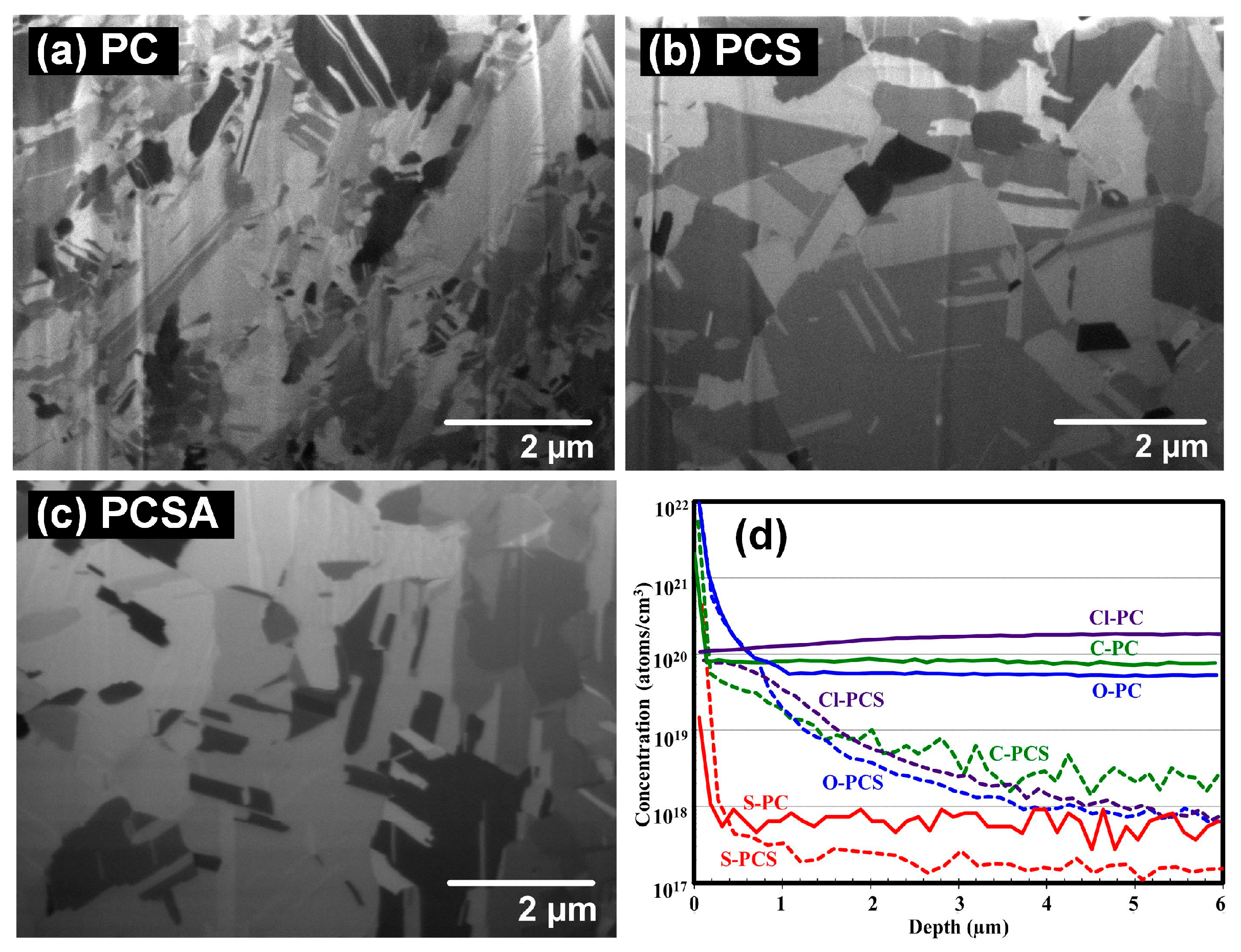
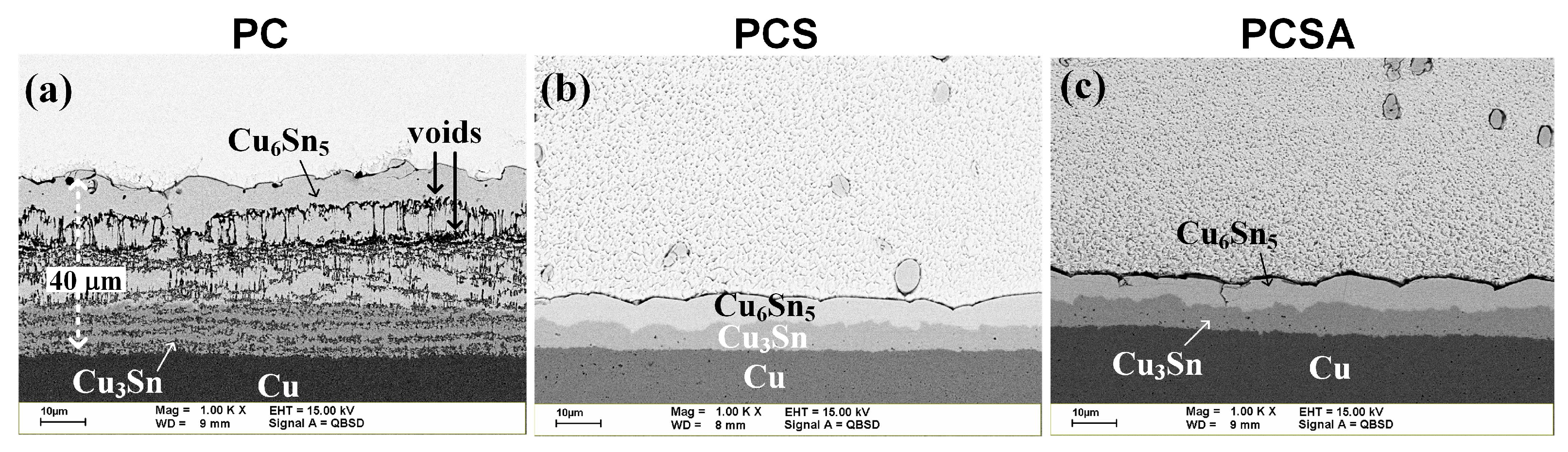
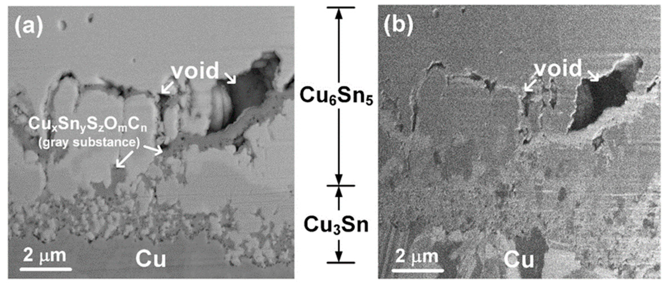
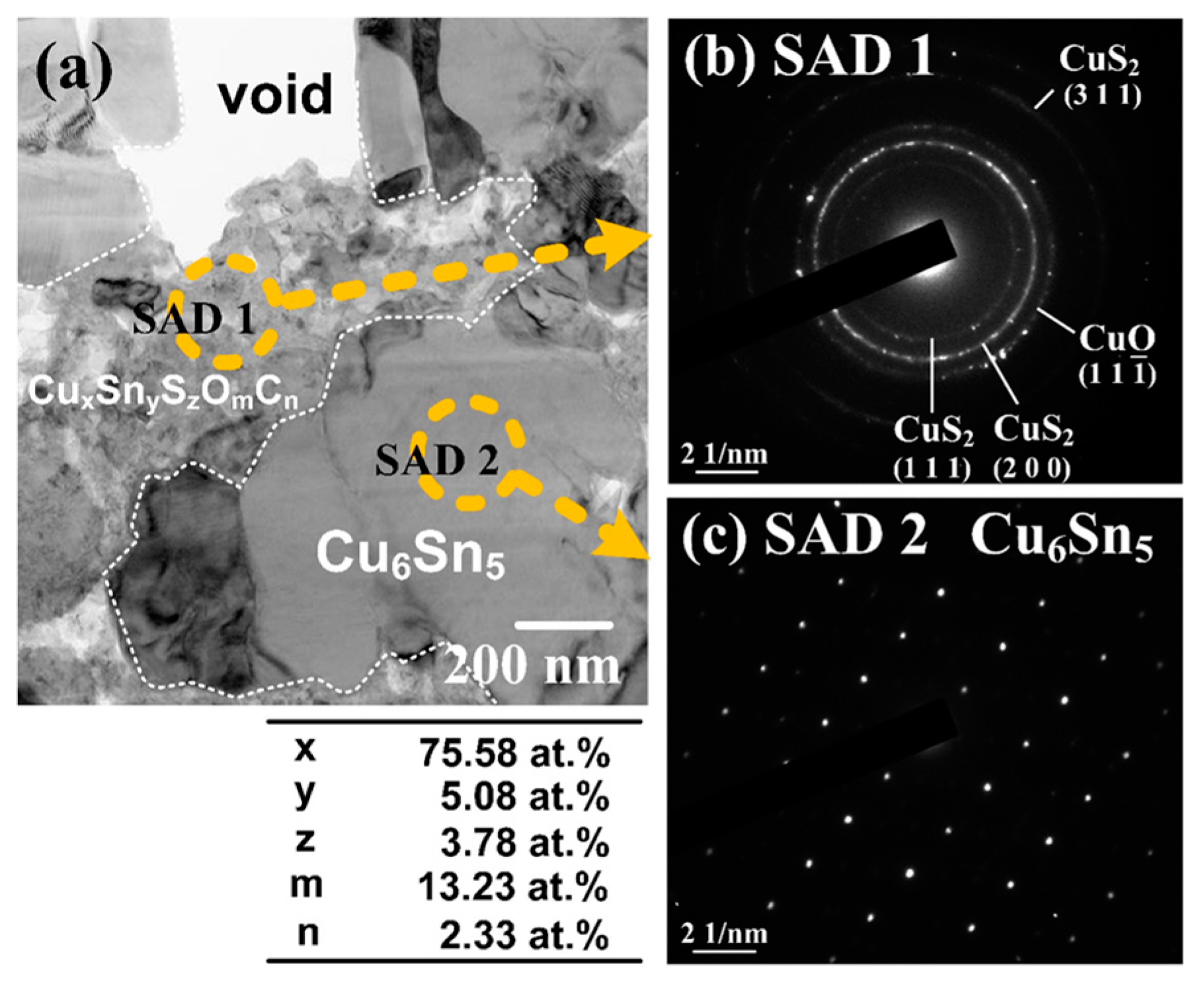
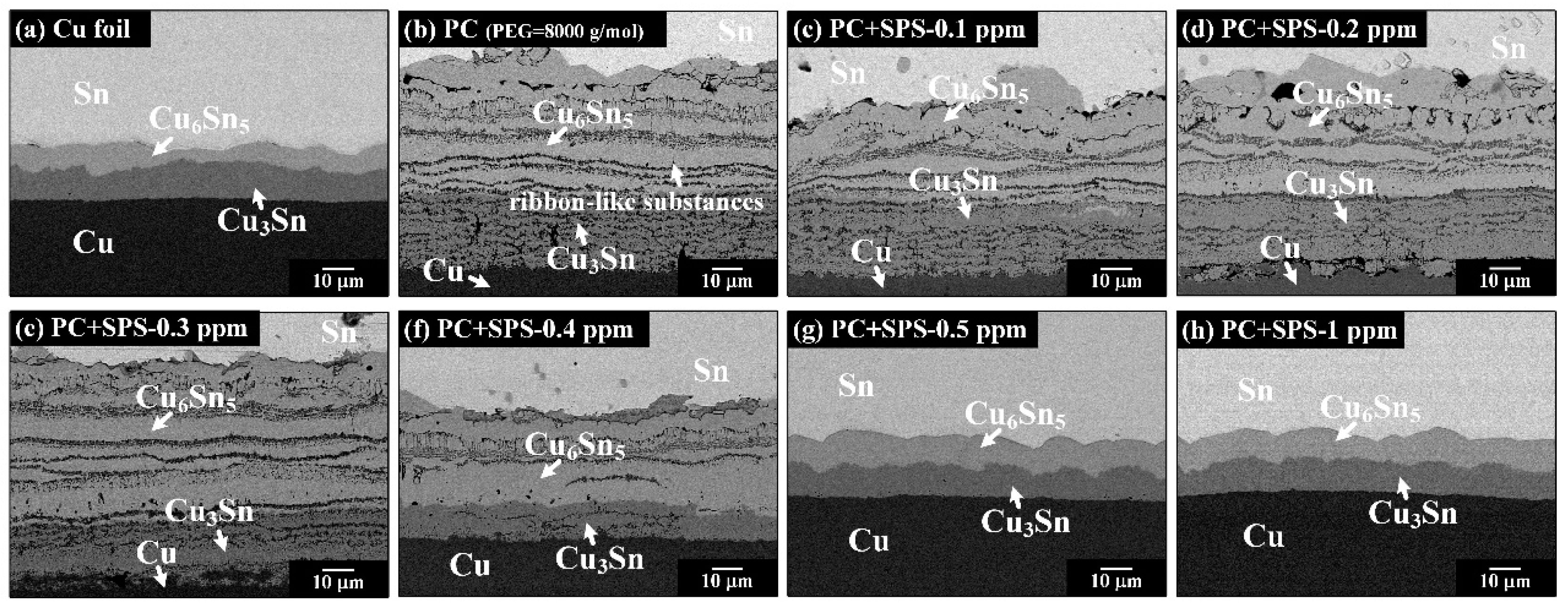
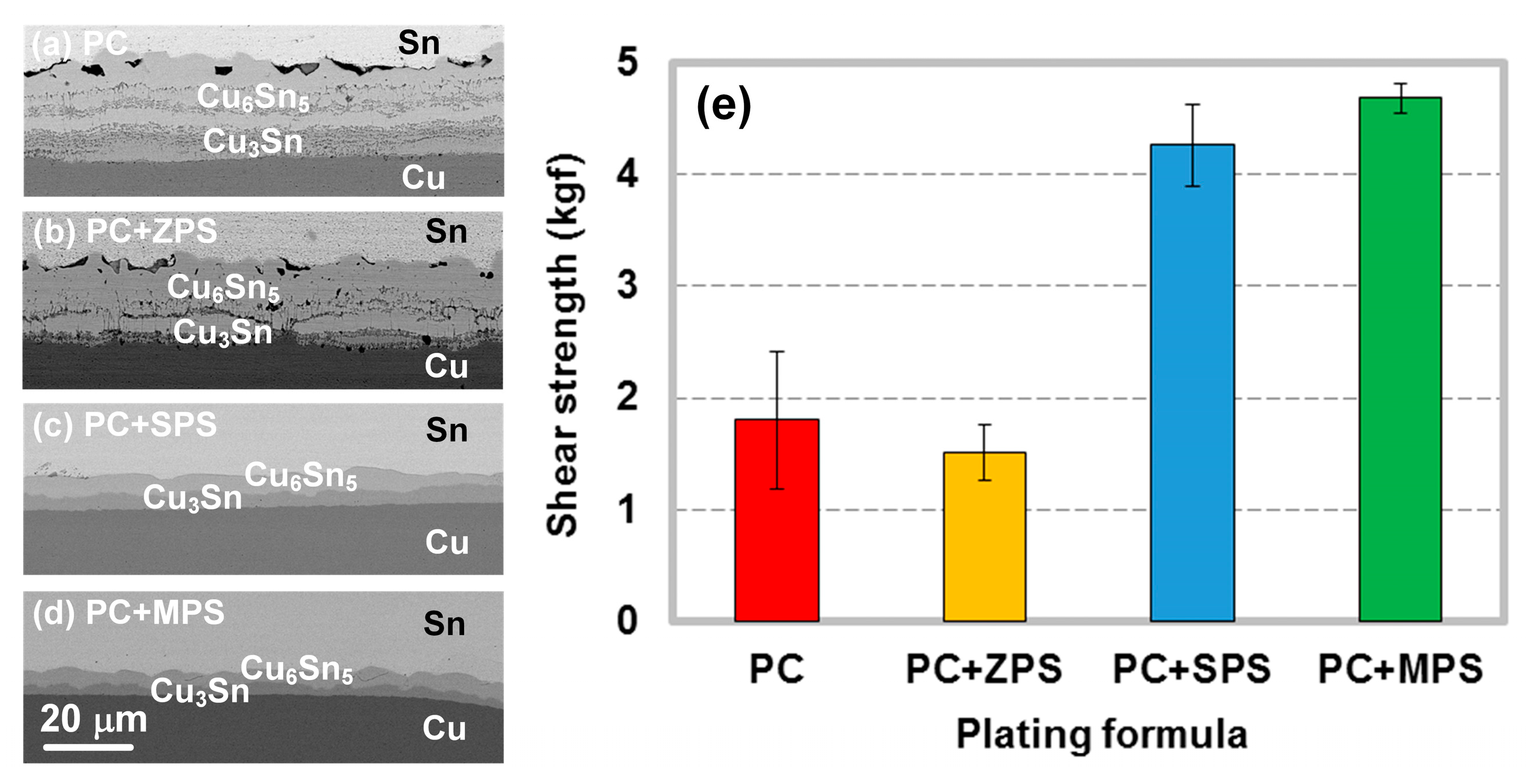
3. Effects of Impurity on Interfacial Reactions of Electroplated-Cu Solder Joints

In the previous section, we have reviewed that the use of functional additives in the electroplating process results in an impurity incorporation in the electroplated Cu layer. Once the impurity content is high (1018–1020 atoms/cm3, depending on the impurity type), it will significantly affect the electrical property and microstructural evolution of the Cu layer [19,21,53,54]. In this section, we will review that the impurity incorporation in the electroplated Cu layer also has a significant effect on the interfacial reactions at the solder/Cu joints.
In 2008, Yu and Kim [29] reported that the use of a high level of SPS (3 × 10⁻⁵ M) combined with basic electrolytes (1 M CuSO4·H2O and 0.7 M H2SO4) caused a considerable amount of impurity residue (sulfur) at the joint interface between Sn–3%Ag–0.5%Cu solder and plated Cu after thermal annealing at 150 °C for 240 h. Redistribution of sulfur towards the solder/Cu interface induced the formation of voids there, which caused the Cu3Sn phase to cease growing, by blocking the diffusion of Cu to the solder side. However, the atomic supply of Sn from the solder continued so the Cu3Sn phase eventually transformed into the Sn-rich Cu6Sn5 phase, leaving only the Cu6Sn5 phase at the interface. Ball shear test showed that the fracture propagated along the Cu6Sn5/Cu interface, where a considerable number of voids were formed. Microanalysis showed that the fracture surface on the Cu side contained a high level of sulfur residue, implying a strong correlation between impurity residue and void formation. By contrast, no impurity residue and void formation were observed when a rolled Cu foil (without additives) was used to join the solder. Yu’s group [57] further proposed a potential method by adding minor sulfide-forming element (0.5 wt. % Zn, Mn, or Cr) in the Pb-free solder to suppress the void formation in the solder joint. They suggested that the sulfide-forming element diffused to the joint interface, and reduced the segregation of S by scavenging S, which effectively suppressed the void formation, and therefore, improved the drop test reliability.
Dimitrov’s group [16,17,33,34,35] also studied the impurity effect since 2008 by using various additive combinations including PEG, SPS, and Cl. The individual use of PEG or Cl resulted in a lower overpotential in the electrodeposition of Cu, but the use of PEG + Cl (nominated as PC) caused an increment in the overpotential, showing that PEG is a suppressor and needs to co-work with the Cl ions. A considerable number of voids were formed at the joint interface when the PC-plated Cu/solder joint was subjected to thermal aging. By contrast, very few voids were observed in the other two cases (individually PEG or Cl). When SPS was additionally added in the plating bath, the overpotential decreased with time, indicating that SPS replaced the adsorption sites of PEG, and therefore accelerated the deposition rate of Cu, due to acceleration ability of SPS. Such competitive adsorption between SPS and PEG generates a synergy capable of suppressing the incorporation of adhesive additives in the electroplated Cu layer. As a result, the impurity residues are effectively suppressed, as well as void formation. The same group continued to investigate the effect of plating current density, and compared the impurity content incorporated in the electroplated Cu layers by using SIMS analysis. In the PC case, a higher plating current density (10 mA/cm2) produced a Cu-plated layer containing a higher level of impurity residues, which led to severe void formation at the resultant solder/Cu interface subjected to thermal annealing. When the plating current density was reduced to 0.5 mA/cm2, the impurity content was greatly reduced, and the solder/Cu interface became void-free. However, the PCS (PEG + Cl + SPS) case showed an opposite trend with the change of current density. The higher the plating current density, the lower the impurity content in the Cu-plated layer. Therefore, the void density was greatly reduced at the solder/Cu interface at a higher current density. The root cause for such an opposite dependence of impurity content and voiding on current density in the PC and PCS cases still remains unclear, and needs more investigation. Dimitrov’s group also investigated the aging effect of plating solution with two additive formulas, PC and PCS. After electroplating at a current density of 10 mA/cm2 for 2, 8, and 18 h, the two additive formulas showed opposite behavior in the overpotential response, due to their opposite effects on the deposition of Cu. In the case of PC, the overpotential decreased with aging time, implying that the suppression effect of PEG became weak due to decomposition of PEG molecules in the acidic environment [35]. Similarly, SPS molecules also degraded with increasing the aging time, but caused the overpotential to increase instead in the PCS case. The competitive adsorption effect became weak due to aging-induced SPS degradation, and therefore, more impurity residues were incorporated in the Cu-plated layer, which resulted in a voiding interface. The above results show that the aging effect on SPS is more pronounced than on PEG.
Recently, our group published a series of papers exploring the effects of additive formulas on the impurity level in the Cu-plated layer and the interfacial reactions in the Sn/Cu joints [18,30,31]. First, three additive formulas were tested including PC, PCS, and PCSA (A is an abbreviation of leveler “ABPV”) with a plating current density of 32 A/ft2 (34.44 mA/cm2) [30]. As shown in Figure 5, the PC-based plating solution produced a Cu layer whose interior grain morphology was irregular. When SPS was added in the plating bath together with PEG and Cl (the formula is PCS), the as-plated Cu layer displayed a more uniform and faceted grain morphology. The PCSA-based plating solution also produced a uniform and faceted grain morphology as PCS did. Based on the SIMS analysis (Figure 5d), the PC-plated Cu layer contained a higher level of impurity residues (carbon, oxygen, chlorine, sulfur), which was two orders of magnitude higher than the PCS-plated Cu. Although the PC formula contained no sulfur-based additive such as SPS, the resultant Cu-plated layer contained a higher level of sulfur than that of PCS which contained SPS. This implies that the source of sulfur is sulfuric acid or copper sulfate from the basic electrolyte, rather than SPS. This also implies that the use of a low level of SPS (2 ppm) causes a negligible impurity incorporation in the Cu-plated layer (Figure 5d). Our group also investigated the interfacial reactions between solder and three plated Cu substrates subjected to thermal aging at 200 °C [30]. As shown in Figure 6, a common Cu6Sn5/Cu3Sn dual-layer structure without noticeable voids was formed at the interfaces where the Cu substrates were electroplated using the formulas of PCS and PCSA (Figure 6b,c). However, an unusual ribbon-like structure was formed in the interfacial IMC layers on the PC-plated Cu substrate (Figure 6a). As mentioned above, the PC-plated Cu substrate contained a higher level of impurity residues, so there should be a strong correlation between the unusual ribbon-like structure and the impurity residues. A high-magnification micrograph shows that the ribbon-like structure is composed of voids, and a gray substance which is identified to contain several elements (copper, tin, sulfur, oxygen, carbon), as shown in Figure 7 [31]. To have a clear understanding of the gray substance, a cross-sectional thin-film sample of the Sn/Cu joint was prepared using FIB, and examined using transmission electron microscopy (TEM). As shown in Figure 8a, the gray substance (marked by SAD1) has a loose structure due to its semi-transparency, and was identified as a mixture composed of nanosized CuO and CuS2 crystals, based on the selected area electron diffraction (SAD) pattern (Figure 8b). This indicates that a high level of impurity residues in the Cu-plated layer participated in the interfacial reactions between solder and Cu and formed the Cu-impurity compounds (CuO and CuS2) within the IMC layer. The presence of impurities might also cause an elimination of vacancy sinks by occupying grain boundary or dislocation, making a significant increase in vacancy concentration. Once the vacancy concentration is oversaturated, voids were formed. It was found that the location of voids closely accompanied the Cu-impurity compounds (Figure 8a), so we believe that this is a strong evidence to support the validity of vacancy sink elimination by impurity.
According to the above results, the synergy resulting from the interaction (competitive adsorption) between PEG (Cl) and SPS plays a crucial role in suppressing the impurity incorporation and void formation at the solder/plated-Cu interface. Our group purposely changed the concentration of SPS, and found that SPS had a threshold concentration beyond which the synergy could work [18]. As shown in Figure 9, the ribbon-like structure was formed at the Sn/Cu interface as the concentration of SPS was below 0.4 ppm, where the molecular weight of PEG is 8000 g/mole and its concentration is 50 ppm. When SPS exceeds 0.5 ppm and above, the ribbon-like structure disappeared, and the interface recovered to a void-free Cu6Sn5/Cu3Sn dual-layer structure. The corresponding SIMS analysis (Figure 10) shows that the impurity concentration has a significant drop as the concentration of SPS increases to 0.4 ppm. At this concentration, the density of ribbon-like structure also greatly decreases, implying that an increase of the SPS concentration is able to reduce the impurity concentration in the Cu-plated layer. Obviously, the threshold concentration of SPS is 0.5 ppm because the solder/Cu interface is free of the ribbon-like structure. The threshold concentration of SPS is also molecular weight of PEG dependent, i.e., the higher the molecular weight of PEG, the higher the threshold concentration of SPS [18]. When the molecular weight of PEG increases, the adsorption sites increase. Therefore, more SPS molecules are needed to compete with PEG to reduce the incorporation of the additives in the growing Cu layer. The formation of the ribbon-like structure is also affected by the thermal aging temperature [18]. As mentioned above, the ribbon-like structure was observed at 200 °C, at which the diffusion of Sn became dominant because the aging temperature was very close to the melting point of Sn. After voids accumulated at the Sn/Cu interface, the downward diffusion of Sn resulted in the formation of IMCs (Cu6Sn5/Cu3Sn) underneath the interfacial voids, i.e., at the Cu side. New voids continued to form at the IMC/Cu interface, and subsequently, new IMCs formed underneath the new interfacial voids due to the dominant diffusion of Sn. The abovementioned formation of interfacial voids and IMCs occurred periodically, leading to the formation of an alternating ribbon-like structure (Figure 6a and Figure 9). The earliest time for the formation of the ribbon-like structure reported in the literature was 72 h at 200 °C [18]. However, when the aging temperature was reduced to 150 °C, the diffusion of Sn became sluggish, as did the growth of the IMCs at the Cu side. The IMCs mainly grew at the Sn side due to the diffusion of Cu toward Sn. Since the impurity incorporation in the Sn is negligible, voids hardly form at the Sn side. As a result, no ribbon-like structure was observed after thermal aging at 150 °C for 600 h. Detailed discussion of the dominant diffusion of Sn at 200 °C and the effect of temperature on the ribbon-like structure can be found in [18]. Yu’s group reported that the ribbon-like structure can also form at 150 °C, and they explained the peculiar IMC growth behavior by the mechanism of secondary IMC formation [58]. Yu and co-worker found the formation of the ribbon-like structure after thermal aging at 150 °C for a much longer time period of 1500–2000 h. In their study, a high level of SPS (3 × 10⁻⁵ M) was used which caused a considerable amount of sulfur residue at the solder/Cu interface.
In addition to SPS, MPS, and ZPS are also common organosulfides that are promising as accelerators. Lee et al. prepared different plating formulas by using different organosulfides as accelerator [31]. They found that the additive formula of PEG + Cl + ZPS (PC + ZPS) resulted in a high impurity level in the Cu-plated layer, which caused the microstructural instability of the Sn/Cu joints in the annealing process (Figure 11b). This case is similar to the abovementioned PC (PEG + Cl) one, where a ribbon-like structure composed of voids and Cu-impurity compounds (CuO and CuS2) was formed within the IMC layer (Figure 11a). However, no ribbon-like structure was observed when the additive formulas changed to PEG + Cl + SPS (PC + SPS) and PEG + Cl + MPS (PC + MPS) as shown in Figure 11c,d. Analysis of cyclic voltammetry (CV) indicates that MPS and SPS are effective accelerators at a 2 ppm concentration but ZPS is not. Figure 3 shows the molecular structures of the three accelerators. The weak acceleration ability of ZPS is attributed to its poor adsorption ability on the growing Cu deposit, due to its benzothiazolyl head group, which acts as a geometrical barrier. By contrast, MPS and SPS have stronger adsorption ability, due to their thiol (R–S–H) and disulfide (R–S–S–R) functional groups, respectively. Therefore, they can effectively adsorb onto the growing Cu deposits, compete with PEG, and suppress the impurity incorporation in the Cu-plated layer. The above results show that the molecular structure of accelerator is also an influential factor in the impurity incorporation in the Cu-plated layer, and the microstructural stability of the solder joints. Because the shear strength of the solder joint was greatly lowered due to formation of voids and Cu-impurity compounds at the joint interface (Figure 11e), a high level of impurity content in the Cu-plated layer is detrimental to the mechanical property of the solder joint. Therefore, precise control or even effective suppression of impurity incorporation in the Cu-plated layer is an important reliability issue for advanced microelectronic solder joints.

4. Conclusions

In this study, a review of the impurity incorporation in the electroplated Cu films originating from the use of organic additives in the plating bath and its effects on the microstructural evolution and void formation in the electroplated-Cu solder joints was carried out. The plating parameters and plating solution chemistry play an important role in the impurity incorporation in the electroplated Cu film. The plating parameters, such as plating current density, plating mode (direct or pulse), and solution aging, are all influential. Moreover, the influences of the plating parameters are additive dependent. For example, the aged plating solution containing an accelerator (SPS) is prone to a high level of impurity incorporation, but that containing a suppressor (PEG) produces a Cu film incorporated a lower level of impurities, because the adsorption strength of PEG molecules on the Cu surface reduces due to aging-induced molecular decomposition. The effect of plating current density on the impurity incorporation is also opposite for PEG and SPS. The plating solution chemistry, such as additive formula, is a complicated factor, and depends upon the competitive adsorption interaction among various additives on the Cu surface. Basically, the use of only suppressor (PEG + Cl) results in the formation of an adhesive polymer monolayer on the growing Cu film. In the electroplating process, the deposition of the Cu atoms inevitably results in an incorporation of the polymer monolayer (or its derivatives) and electrolyte ions ( SO 4 2 ) in the electroplated Cu film, leading to a high-level impurity concentration (C, O, Cl, and S). A high level of impurity incorporation in the electroplated Cu film may inhibit self-annealing of Cu due to Zener pinning effect, and fails to reduce the electrical resistivity. Segregation of impurity toward the film surface may cause the pinhole formation. When the “impure” Cu film is joined to solder (Sn) to form a solder joint, segregation of the derivatives of suppressor occurs in the thermal aging process which annihilates the vacancy sinks, such as dislocation and grain boundary, and therefore accelerates the oversaturation of vacancy to form voids in the solder joint. The incorporated impurities even react with Cu to form the Cu-impurity compounds in the periphery of voids. Addition of an accelerator (SPS) in the plating bath, along with the suppressor (PEG + Cl), generates a synergy capable of destroying the adsorption of suppressor on the Cu film through a competitive adsorption mechanism dominated by SPS. As a result, the use of both suppressor and accelerator effectively suppresses the impurity incorporation, and therefore suppresses void formation in the solder joints. However, the competitive adsorption capability of SPS is strongly concentration dependent. A critical concentration of SPS can be experimentally determined, above which the competitive adsorption effect can work. The competitive adsorption capability of accelerator is also dominated by its molecular structure. In addition to SPS with a disulfide (R–S–S–R) group, MPS is also an effective accelerator with a thiol (R–S–H) functional group, which can adsorb firmly on the film surface and compete with PEG to suppress the impurity incorporation. B contrast, ZPS is a weak accelerator, and its poor accelerating effect is ascribed to a benzothiazolyl head group which acts as a geometrical barrier to hinder effective adsorption of accelerator.

Author Contributions

C.-M.C. wrote the manuscript and supervised the whole study. H.L. conducted the literature collection and research. All authors reviewed the final paper.

Funding

This research was funded by the Ministry of Education and the Ministry of Science and Technology in Taiwan (MOST 105-2221-E-005-087).

Acknowledgments

This work was financially supported by the “Innovation and Development Center of Sustainable Agriculture” from The Featured Areas Research Center Program within the framework of the Higher Education Sprout Project by the Ministry of Education (MOE) in Taiwan. This work was also financially supported by the Ministry of Science and Technology (105-2221-E-005-087) in Taiwan.

Conflicts of Interest

The authors declare no conflict of interest.

References

  1. Andricacos, P.C.; Uzoh, C.; Dukovic, J.O.; Horkans, J.; Deligianni, H. Damascene copper electroplating for chip interconnections. IBM J. Res. Dev. 1998, 42, 567–574. [Google Scholar] [CrossRef]
  2. Van Olmen, J.; Huyghebaert, C.; Coenen, J.; Van Aelst, J.; Sleeckx, E.; Van Ammel, A.; Armini, S.; Katti, G.; Vaes, J.; Dehaene, W. Integration challenges of copper through silicon via (TSV) metallization for 3D-stacked IC integration. Microelectron. Eng. 2011, 88, 745–748. [Google Scholar] [CrossRef]
  3. Hofmann, L.; Ecke, R.; Schulz, S.E.; Gessner, T. Investigations regarding through silicon via filling for 3D integration by periodic pulse reverse plating with and without additives. Microelectron. Eng. 2011, 88, 705–708. [Google Scholar] [CrossRef]
  4. Moffat, T.; Josell, D. Extreme bottom-up superfilling of through-silicon-vias by damascene processing: Suppressor disruption, positive feedback and turing patterns. J. Electrochem. Soc. 2012, 159, D208–D216. [Google Scholar] [CrossRef]
  5. Sun, J.-J.; Kondo, K.; Okamura, T.; Oh, S.; Tomisaka, M.; Yonemura, H.; Hoshino, M.; Takahashi, K. High-aspect-ratio copper via filling used for three-dimensional chip stacking. J. Electrochem. Soc. 2003, 150, G355–G358. [Google Scholar] [CrossRef]
  6. Dow, W.-P.; Yen, M.-Y.; Lin, W.-B.; Ho, S.-W. Influence of molecular weight of polyethylene glycol on microvia filling by copper electroplating. J. Electrochem. Soc. 2005, 152, C769–C775. [Google Scholar] [CrossRef]
  7. Feng, Z.V.; Li, X.; Gewirth, A.A. Inhibition due to the interaction of polyethylene glycol, chloride, and copper in plating baths: A surface-enhanced raman study. J. Phys. Chem. B 2003, 107, 9415–9423. [Google Scholar] [CrossRef]
  8. Kelly, J.J.; West, A.C. Copper deposition in the presence of polyethylene glycol I. Quartz crystal microbalance study. J. Electrochem. Soc. 1998, 145, 3472–3476. [Google Scholar] [CrossRef]
  9. Hayase, M.; Taketani, M.; Aizawa, K.; Hatsuzawa, T.; Hayabusa, K. Copper bottom-up deposition by breakdown of PEG-Cl inhibition. Electrochem. Solid State Lett. 2002, 5, C98–C101. [Google Scholar] [CrossRef]
  10. Beica, R.; Sharbono, C.; Ritzdorf, T. Through silicon via copper electrodeposition for 3D integration. In Proceedings of the 58th Electronic Components and Technology Conference, ECTC 2008, Lake Buena Vista, FL, USA, 27–30 May 2008; IEEE: Piscataway, NJ, USA, 2008; pp. 577–583. [Google Scholar]
  11. Chiu, Y.-D.; Dow, W.-P. Accelerator screening by cyclic voltammetry for microvia filling by copper electroplating. J. Electrochem. Soc. 2013, 160, D3021–D3027. [Google Scholar] [CrossRef]
  12. Tan, M.; Harb, J.N. Additive behavior during copper electrodeposition in solutions containing Cl, PEG, and SPS. J. Electrochem. Soc. 2003, 150, C420–C425. [Google Scholar] [CrossRef]
  13. Jin, Y.; Sui, Y.; Wen, L.; Ye, F.; Sun, M.; Wang, Q. Competitive adsorption of PEG and SPS on copper surface in acidic electrolyte containing Cl. J. Electrochem. Soc. 2013, 160, D20–D27. [Google Scholar] [CrossRef]
  14. Farndon, E.E.; Campbell, S.A.; Walsh, F.C. Effect of thiourea, benzotriazole and 4,5-dithiaoctane-1,8-disulphonic acid on the kinetics of copper deposition from dilute acid sulfate solutions. J. Appl. Electrochem. 1995, 25, 574–583. [Google Scholar] [CrossRef]
  15. Kelly, J.J.; West, A.C. Copper deposition in the presence of polyethylene glycol II. Electrochemical impedance spectroscopy. J. Electrochem. Soc. 1998, 145, 3477–3481. [Google Scholar] [CrossRef]
  16. Liu, Y.; Wang, J.; Yin, L.; Kondos, P.; Parks, C.; Borgesen, P.; Henderson, D.; Cotts, E.; Dimitrov, N. Influence of plating parameters and solution chemistry on the voiding propensity at electroplated copper-solder interface. J. Appl. Electrochem. 2008, 38, 1695–1705. [Google Scholar] [CrossRef]
  17. Liu, Y.; Yin, L.; Bliznakov, S.; Kondos, P.; Borgesen, P.; Henderson, D.W.; Parks, C.; Wang, J.; Cotts, E.J.; Dimitrov, N. Improving copper electrodeposition in the microelectronics industry. IEEE Trans. Compon. Packag. Technol. 2010, 33, 127–137. [Google Scholar] [CrossRef]
  18. Yu, T.-Y.; Lee, H.; Hsu, H.-L.; Dow, W.-P.; Cheng, H.-K.; Liu, K.-C.; Chen, C.-M. Effects of Cu electroplating formulas on the interfacial microstructures of Sn/Cu joints. J. Electrochem. Soc. 2016, 163, D734–D741. [Google Scholar] [CrossRef]
  19. Stangl, M.; Acker, J.; Oswald, S.; Uhlemann, M.; Gemming, T.; Baunack, S.; Wetzig, K. Incorporation of sulfur, chlorine, and carbon into electroplated Cu thin films. Microelectron. Eng. 2007, 84, 54–59. [Google Scholar] [CrossRef]
  20. Reed-Hill, R.E.; Abbaschian, R. Physical Metallurgy Principles, 3rd ed.; PWS Publishing Company: Boston, MA, USA, 1994; pp. 262–263. ISBN 0-534-92173-6. [Google Scholar]
  21. Chen, C.-C.; Hsieh, C.-H.; Lee, Y.-W.; Yang, C.-H.; Ho, C.-E. Formation mechanism of pinholes in electroplated Cu films and its mitigation. Thin Solid Films 2015, 596, 209–215. [Google Scholar] [CrossRef]
  22. Cheng, H.-K.; Huang, C.-W.; Lee, H.; Wang, Y.-L.; Liu, T.-F.; Chen, C.-M. Interfacial reactions between Cu and SnAgCu solder doped with minor Ni. J. Alloys Compd. 2015, 622, 529–534. [Google Scholar] [CrossRef]
  23. Lin, C.-P.; Chen, C.-M.; Yen, Y.-W. Enhanced growth of the Cu6Sn5 phase in the Sn/Ag/Cu and Sn/Cu multilayers subjected to applied strain. J. Alloys Compd. 2014, 591, 297–303. [Google Scholar] [CrossRef]
  24. Zeng, K.; Stierman, R.; Chiu, T.-C.; Edwards, D.; Ano, K.; Tu, K. Kirkendall void formation in eutectic SnPb solder joints on bare Cu and its effect on joint reliability. J. Appl. Phys. 2005, 97, 024508. [Google Scholar] [CrossRef]
  25. Wang, Y.-W.; Lin, Y.; Kao, C.R. Kirkendall voids formation in the reaction between Ni-doped snag lead-free solders and different Cu substrates. Microelectron. Reliab. 2009, 49, 248–252. [Google Scholar] [CrossRef]
  26. Ho, C.E.; Kuo, T.T.; Wang, C.C.; Wu, W.H. Inhibiting the growth of Cu3Sn and kirkendall voids in the Cu/Sn-Ag-Cu system by minor Pd alloying. Electron. Mater. Lett. 2012, 8, 495–501. [Google Scholar] [CrossRef]
  27. Wang, Y.; Lin, Y.; Tu, C.; Kao, C. Effects of minor Fe, Co, and Ni additions on the reaction between SnAgCu solder and Cu. J. Alloys Compd. 2009, 478, 121–127. [Google Scholar] [CrossRef]
  28. Yin, L.; Borgesen, P. On the root cause of kirkendall voiding in Cu3Sn. J. Mater. Res. 2011, 26, 455–466. [Google Scholar] [CrossRef]
  29. Yu, J.; Kim, J. Effects of residual S on kirkendall void formation at Cu/Sn–3.5Ag solder joints. Acta Mater. 2008, 56, 5514–5523. [Google Scholar] [CrossRef]
  30. Wu, J.-Y.; Lee, H.; Wu, C.-H.; Lin, C.-F.; Dow, W.-P.; Chen, C.-M. Effects of electroplating additives on the interfacial reactions between Sn and Cu electroplated layers. J. Electrochem. Soc. 2014, 161, D522–D527. [Google Scholar] [CrossRef]
  31. Lee, H.; Yu, T.-Y.; Cheng, H.-K.; Liu, K.-C.; Chan, P.-F.; Dow, W.-P.; Chen, C.-M. Impurity incorporation in the Cu electrodeposit and its effects on the microstructural evolution of the Sn/Cu solder joints. J. Electrochem. Soc. 2017, 164, D457–D462. [Google Scholar] [CrossRef]
  32. Ross, G.; Vuorinen, V.; Paulasto-Kröckel, M. Void formation and its impact on CuSn intermetallic compound formation. J. Alloys Compd. 2016, 677, 127–138. [Google Scholar] [CrossRef]
  33. Wafula, F.; Liu, Y.; Yin, L.; Bliznakov, S.; Borgesen, P.; Cotts, E.; Dimitrov, N. Impact of key deposition parameters on the voiding sporadically occurring in solder joints with electroplated copper. J. Electrochem. Soc. 2010, 157, D111–D118. [Google Scholar] [CrossRef]
  34. Wafula, F.; Liu, Y.; Yin, L.; Borgesen, P.; Cotts, E.; Dimitrov, N. Effect of the deposition parameters on the voiding propensity of solder joints with Cu electroplated in a hull cell. J. Appl. Electrochem. 2011, 41, 469–480. [Google Scholar] [CrossRef]
  35. Wafula, F.; Yin, L.; Borgesen, P.; Andala, D.; Dimitrov, N. Influence of poly(ethylene glycol) degradation on voiding sporadically occurring in solder joints with electroplated Cu. J. Electron. Mater. 2012, 41, 1898–1906. [Google Scholar] [CrossRef]
  36. Cheng, H.K.; Lin, Y.J.; Chen, C.M.; Liu, K.C.; Wang, Y.L.; Liu, T.F. Microstructural evolution of Cu/solder/Cu pillar-type structures with different diffusion barriers. Metall. Mater. Trans. A 2016, 47, 3971–3980. [Google Scholar] [CrossRef]
  37. Jones, T.D.A.; Bernassau, A.; Flynn, D.; Price, D.; Beadel, M.; Desmulliez, M.P.Y. Copper electroplating of PCB interconnects using megasonic acoustic streaming. Ultrason. Sonochem. 2018, 42, 434–444. [Google Scholar] [CrossRef] [PubMed]
  38. Yokoi, M. Copper Electrodepositon. In Copper Electrodeposition for Nanofabrication of Electronics Devices, Nanostructure Science and Technology; Kondo, K., Akolkar, R.N., Barkey, D.P., Yokoi, M., Eds.; Springer: New York, NY, USA, 2014; pp. 3–25. [Google Scholar]
  39. Dow, W.-P.; Huang, H.-S.; Yen, M.-Y.; Huang, H.-C. Influence of convection-dependent adsorption of additives on microvia filling by copper electroplating. J. Electrochem. Soc. 2005, 152, C425–C434. [Google Scholar] [CrossRef]
  40. Kondo, K.; Matsumoto, T.; Watanabe, K. Role of additives for copper damascene electrodeposition experimental study on inhibition and acceleration effects. J. Electrochem. Soc. 2004, 151, C250–C255. [Google Scholar] [CrossRef] [Green Version]
  41. Reid, J. Copper electrodeposition: Principles and recent progress. Jpn. J. Appl. Phys. 2001, 40, 2650–2657. [Google Scholar] [CrossRef]
  42. Wang, W.; Li, Y.-B. Effect of Cl on the adsorption-desorption behavior of PEG. J. Electrochem. Soc. 2008, 155, D263–D269. [Google Scholar] [CrossRef]
  43. Moffat, T.P.; Wheeler, D.; Josell, D. Electrodeposition of copper in the SPS-PEG-Cl additive system I. Kinetic measurements: Influence of SPS. J. Electrochem. Soc. 2004, 151, C262–C271. [Google Scholar] [CrossRef]
  44. Gallaway, J.W.; West, A.C. PEG, PPG, and their triblock copolymers as suppressors in copper electroplating. J. Electrochem. Soc. 2008, 155, D632–D639. [Google Scholar] [CrossRef]
  45. Choe, S.; Kim, M.J.; Kim, H.C.; Cho, S.K.; Ahn, S.H.; Kim, S.-K.; Kim, J.J. Degradation of bis (3-sulfopropyl) disulfide and its influence on copper electrodeposition for feature filling. J. Electrochem. Soc. 2013, 160, D3179–D3185. [Google Scholar] [CrossRef]
  46. Chen, T.-C.; Tsai, Y.-L.; Hsu, C.-F.; Dow, W.-P.; Hashimoto, Y. Effects of brighteners in a copper plating bath on throwing power and thermal reliability of plated through holes. Electrochim. Acta 2016, 212, 572–582. [Google Scholar] [CrossRef]
  47. Hau-Riege, S.P.; Thompson, C.V. In situ transmission electron microscope studies of the kinetics of abnormal grain growth in electroplated copper films. Appl. Phys. Lett. 2000, 76, 309–311. [Google Scholar] [CrossRef]
  48. Lagrange, S.; Brongersma, S.; Judelewicz, M.; Saerens, A.; Vervoort, I.; Richard, E.; Palmans, R.; Maex, K. Self-annealing characterization of electroplated copper films. Microelectron. Eng. 2000, 50, 449–457. [Google Scholar] [CrossRef]
  49. Ho, C.-E.; Chen, C.-C.; Lu, M.-K.; Lee, Y.-W.; Wu, Y.-S. In-situ study on the self-annealing behavior of electroplated Cu through the cantilever method, XRD, and EBSD. Surf. Coat. Technol. 2016, 303, 86–93. [Google Scholar] [CrossRef]
  50. Harper, J.; Cabral, C., Jr.; Andricacos, P.; Gignac, L.; Noyan, I.; Rodbell, K.; Hu, C. Mechanisms for microstructure evolution in electroplated copper thin films near room temperature. J. Appl. Phys. 1999, 86, 2516–2525. [Google Scholar] [CrossRef]
  51. Cheng, M.-Y.; Chen, K.-W.; Liu, T.-F.; Wang, Y.-L.; Feng, H.-P. Effects of direct current and pulse-reverse copper plating waveforms on the incubation behavior of self-annealing. Thin Solid Films 2010, 518, 7468–7474. [Google Scholar] [CrossRef]
  52. Strehle, S.; Reiche, R.; Hoffmann, V.; Acker, J.; Gemming, T.; Wetzig, K. Sulfur incorporation in electroplated Cu (Ag) thin films. Microchim. Acta 2006, 156, 167–172. [Google Scholar] [CrossRef]
  53. Huang, Q.; Avekians, A.; Ahmed, S.; Parks, C.; Baker-O’Neal, B.; Kitayaporn, S.; Sahin, A.; Sun, Y.; Cheng, T. Impurities in the electroplated sub-50 nm Cu lines: The effects of the plating additives. J. Electrochem. Soc. 2014, 161, D388–D394. [Google Scholar] [CrossRef]
  54. Kitayaporn, S.; Huang, Q.; Hopstaken, M.; Baker-O’Neal, B. Tin incorporated in copper films during damascene copper electrodeposition. J. Electrochem. Soc. 2015, 162, D74–D81. [Google Scholar] [CrossRef]
  55. Chen, C.-C.; Yang, C.-H.; Wu, Y.-S.; Ho, C.-E. Depth-dependent self-annealing behavior of electroplated Cu. Surf. Coat. Technol. 2017, 320, 489–496. [Google Scholar] [CrossRef]
  56. Lee, P.; Wu, Y.; Lin, P.; Chen, C.; Hsieh, W.; Ho, C. High-speed Cu electrodeposition and its solderability. Surf. Coat. Technol. 2017, 320, 559–567. [Google Scholar] [CrossRef]
  57. Kim, J.; Yu, J.; Kim, S. Effects of sulfide-forming element additions on the kirkendall void formation and drop impact reliability of Cu/Sn-3.5Ag solder joints. Acta Mater. 2009, 57, 5001–5012. [Google Scholar] [CrossRef]
  58. Kim, S.H.; Yu, J. Secondary IMC formation induced by Kirkendall voiding in Cu/Sn-3.5Ag solder joints. J. Mater. Res. 2010, 25, 1854–1858. [Google Scholar] [CrossRef]
Figure 1. Schematic diagram of the adsorption behavior of various additives on the Cu deposit with a blind hole. Suppressor adsorbs on the surface of the Cu deposit outside the hole, which can suppress the deposition rate of Cu outside the hole. Accelerator adsorbs on the bottom of the hole to accelerate the deposition rate of Cu there. Leveler tends to adsorb on the opening area of the hole where the current concentrates, which can suppress the deposition rate of Cu on the hole opening to avoid void formation inside the hole due to fast sealing of the hole opening.
Metals 08 00388 g001
Figure 2. Possible configuration of the PEG–Cu+–Cl complex adsorbed on the surface of the Cu deposit. Adapted with permission from [7], American Chemical Society, 2003.
Metals 08 00388 g002
Figure 3. Typical molecular structures of three accelerators: (a) ZPS, (b) SPS, and (c) MPS. Reproduced with permission from [31], The Electrochemical Society, 2017.
Metals 08 00388 g003
Figure 4. Molecular structure of a commercial leveler, JGB (Janus Green B).
Metals 08 00388 g004
Figure 5. Cross-sectional ion beam images of the grain microstructures of the Cu deposits fabricated using various additive formulas: (a) PEG + Cl (PC), (b) PEG + Cl + SPS (PCS), and (c) PEG + Cl + SPS + ABPV (PCSA). (d) Depth-profile analysis of SIMS of four impurities (C, O, Cl, and S) in the two Cu deposits fabricated using PC and PCS as the additive formulas. Reproduced with permission from [30], The Electrochemical Society, 2014.
Metals 08 00388 g005
Figure 6. Cross-sectional scanning electron microscopy (SEM) micrographs of the Sn/Cu interfaces subjected to thermal aging at 200 °C for 240 h. The Cu substrates in (a), (b), and (c) were fabricated using PEG + Cl (PC), PEG + Cl + SPS (PCS), and PEG + Cl + SPS + ABPV (PCSA), respectively, as the additive formulas. Reproduced with permission from [30], The Electrochemical Society, 2014.
Metals 08 00388 g006
Figure 7. High-magnification cross-sectional SEM micrograph of the Sn/Cu interface after thermal aging at 200 °C, where the Cu substrate was prepared using PEG + Cl (PC) as the additive formula: (a) backscattered electron image, (b) secondary electron image. Reproduced with permission from [31], The Electrochemical Society, 2017.
Metals 08 00388 g007
Figure 8. TEM analysis of the ribbon-like structure formed at the Sn/Cu interface where the Cu substrate was prepared using the PEG + Cl (PC) as the additive formula: (a) bright-field TEM image, (b) SAD pattern of the Cu-impurity compounds (CuO and CuS2), and (c) SAD pattern of the Cu6Sn5 phase. Reproduced with permission from [31], The Electrochemical Society, 2017.
Metals 08 00388 g008
Figure 9. Cross-sectional SEM micrographs of the Sn/Cu interfaces subjected to thermal aging at 200 °C for 600 h, where the Cu substrate in (a) is homemade Cu foil and the others were fabricated using electroplating with a common additive formula of PEG + Cl (PC) but at various SPS concentrations: (b) SPS = 0 ppm, (c) SPS = 0.1 ppm, (d) SPS = 0.2 ppm, (e) SPS = 0.3 ppm, (f) SPS = 0.4 ppm, (g) SPS = 0.5 ppm, and (h) SPS = 1 ppm. Reproduced with permission from [18], The Electrochemical Society, 2016.
Metals 08 00388 g009
Figure 10. Concentration-depth profiles of additive-derived impurities with the change of the SPS concentration: (a) C, (b) S, (c) Cl, and (d) O. Reproduced with permission from [18], The Electrochemical Society, 2016.
Metals 08 00388 g010
Figure 11. Cross-sectional SEM micrographs of the Sn/Cu interfaces subjected to thermal aging at 200 °C for 72 h, where the Cu substrates were prepared using various additive formulas: (a) PC (PEG + Cl), (b) PC + ZPS, (c) PC + SPS, (d) PC + MPS. (e) Shear strength of the aged Sn/Cu solder joints prepared using various additive formulas. Reproduced with permission from [31], The Electrochemical Society, 2017.
Metals 08 00388 g011
Table 1. Concentrations of Cu sulfate (CuSO4) and sulfuric acid (H2SO4) suggested for various applications. Adapted with permission from [38], Springer, 2014.
BathsPrimary Constituents (g/L)Applications
Conventional bathCuSO4·5H2O (180–250)
H2SO4 (60–40)
Decorative plating
Copper refining
Electroforming, etc.
High-through bathCuSO4·5H2O (60–100)Printed wiring board plating
H2SO4 (250–200)Through-hole plating
Via filling bathCuSO4·5H2O (150–230)Build-up PWB plating
H2SO4 (15–50)
Nanoplating bathCuSO4·5H2O (60–100)LSI trench/via filling
H2SO4 (200–10)

