Article

The Effect of Cobalt Incorporation on the Microstructure and Properties of Cu(Co) Alloys for Use in Hybrid Bonding

Department of Nanoscale Science and Engineering, University at Albany, State University of New York, Albany, NY 12203, USA
*
Author to whom correspondence should be addressed.
Metals 2025, 15(9), 1023; https://doi.org/10.3390/met15091023
Submission received: 30 July 2025 / Revised: 31 August 2025 / Accepted: 4 September 2025 / Published: 15 September 2025
(This article belongs to the Special Issue Solidification and Microstructure of Metallic Alloys)

Abstract

In this study, the properties of Cu(Co) alloy films were investigated to assess their utility as an alternative material for interconnections in hybrid bonding applications. Thin films of Cu(Co) were deposited using electrochemical deposition in a standard sulfate-based electrolyte. X-ray photoelectron spectroscopy (XPS) of the films revealed that an increasing current density during deposition resulted in an increase in cobalt concentration. Bright-field scanning transmission electron microscopy (STEM) coupled with energy-dispersive x-ray spectroscopy (EDS) was used to visualize the fine-grained microstructure and confirmed grain boundary segregation of cobalt in the films. X-ray diffraction with a heated stage determined that the coefficient of thermal expansion (CTE) increased linearly with increasing cobalt content, from 17.5 ppm/K for pure copper to a maximum of 27.5 ppm/K for a film containing 24 at.% Co. Nanoindentation experiments found that the mechanical properties depended non-linearly on composition, with hardness increasing from 3.5 GPa for a 0% cobalt film to a maximum of 4.5 GPa (24 at.% Co) and the Young’s modulus increasing from 118 GPa to 214 GPa, respectively. Four-point probe electrical measurements confirmed the expected linear increase in resistivity as Co content increased. Since electrical and mechanical properties have differing dependences on the film composition, an optimal alloy composition that balances an acceptable increase in resistance with improved mechanical properties could enable more reliable, low-temperature bonding solutions in advanced microelectronic devices.

1. Introduction

Hybrid bonding is a key technological innovation in advanced semiconductor packaging, particularly for enabling three-dimensional integration (3DI) in electronic devices. It involves directly joining two wafers or chips at both the dielectric and metal interfaces, creating interconnects that provide electrical, thermal, and mechanical continuity. Unlike traditional bonding methods like wire bonding or solder bump bonding, hybrid bonding eliminates the need for intermediary materials such as micro bumps [1]. This allows for finer pitch interconnects, which reduce signal delay, lower power consumption, and shrink the overall device footprint, while enhancing performance and enabling higher integration density [2,3]. These advantages make hybrid bonding particularly valuable in high-speed computing, memory, and other semiconductor applications.
Despite its benefits, hybrid bonding presents several challenges, particularly in ensuring mechanical stability, precise alignment, and bonding at low temperature [4,5]. Cu-based interconnects, which are commonly used in this process, face several distinct issues. During chemical–mechanical planarization (CMP), the copper surface has a tendency to dish relative to the surrounding dielectric, leaving a gap when two wafers are brought into contact. A relatively high bonding temperature is required for closing this gap, and plastic deformation during bonding can also contribute to misalignment [6,7]. Ensuring mechanical stability and reliability at lower processing temperatures—critical for protecting front-end devices—remains a difficult challenge. To address these concerns, the use of fine-grained copper and/or alloying the copper with other metals are being explored as avenues to overcome the above-mentioned challenges to enable high-performance applications in advanced semiconductor packaging [8,9,10].
In microelectronics, Cu alloys have been explored for their mechanical, electrical, and thermal properties, particularly in environments involving elevated temperatures and high current densities [11,12,13]. Cobalt (Co) is of special interest because of its unique properties and its ability to improve the reliability of Cu interconnects [14,15]. In the back end of the line (BEOL), interconnects fail by surface diffusion or grain boundary diffusion in copper’s polygranular microstructure [16]. Co-containing capping layers can mitigate surface diffusion [17,18,19], while alloying solutes can slow grain boundary diffusion by raising activation energy for atomic motion [20], though their mechanisms and efficacy remain debated. Cobalt inclusion minimally affects grain growth but alters film texture post-recrystallization, which in turn changes the character of the remaining grain boundaries [21,22,23]. Historically, solutes were expected to pin grain boundaries and reduce diffusivity via “stuffing” [24], but studies on grain boundary complexions [25] suggest nuanced orientation-dependent behaviors, which may explain the Co-based data. While cobalt inclusion does raise electrical resistance due to impurity scattering [26], some increase can be tolerated if electromigration resistance improves sufficiently. Therefore, minimizing impurity scattering by confining cobalt to grain boundaries, rather than uniformly distributing it throughout the bulk of the interconnect, is desirable. This appears a reasonable goal for cobalt, as its limited solid solubility in Cu favors grain boundary segregation as a result of repulsion between Cu and Co [22,27].
Previous modelling research indicates that Co may also enable mechanical improvements desired for hybrid bonding. For example, the inclusion of a Co cap on Cu increases the overall CTE of the layered structure due to diffusion [9]. As the thickness of the cap layer increased, the CTE of the full structure initially rose, but then decreased after reaching a maximum value of 43.6%. This behavior suggests tunability for CTE in this system. CTE is critical for the success of hybrid bonding, as post-bond annealing requires Cu pads to expand sufficiently to overcome the dishing gap from CMP, to establish contact and complete the bond. A higher CTE would enable the same degree of expansion at a lower annealing temperature, protecting sensitive structures already in place on the wafer. The expansion depends on both pad volume and annealing temperature, with smaller, primarily elastic expansion observed for equal-sized pads [28]. Such elastic deformation is vital for maintaining bond integrity, as it prevents misalignment and cracking, thereby ensuring a robust connection. Conversely, plastic deformation, where the material undergoes a permanent shape change, can lead to misalignment and reduced yield. To address this, high yield-strength in the Cu pads is essential, as it prevents plastic deformation and ensures the pads undergo controlled elastic deformations, maintaining consistent and reliable bonding. Since alloying changes the mechanical properties of the Cu pads, it may be possible to achieve a balance between these disparate requirements by tuning the alloy composition.
The study investigates the microstructural, mechanical, and electrical properties of Cu–Co alloys, emphasizing how the inclusion of Co influences the coefficient of thermal expansion, hardness, and modulus to mitigate challenges such as misalignment or cracking during the bonding process.

2. Experimental Section

2.1. Film Growth

The co-deposition of Cu–Co alloys by electrochemical deposition (ECD) presents challenges due to the significant difference in reduction potential between Cu and Co. The reduction potential of Co is significantly more cathodic (more negative) than that of Cu. If a voltage more negative than the reduction potential of Co2+ ions is applied in a solution containing Cu2+ ions, the current density for Cu2+ reduction would become excessively high, potentially resulting in rough or poor-quality Cu alloy deposits [29]. To mitigate this issue, a chelating agent (trisodium citrate) was introduced to the solution to lower the effective concentration of Cu2+ ions, helping to balance the deposition process [30]. However, the addition of a chelating agent requires further optimization to ensure uniform deposition of the Cu–Co alloy, as it introduces additional complexity to the process and introduces a potential source of impurity contamination. To prevent any fluctuations in pH during deposition, boric acid was added as a buffering agent. This ensures stable conditions, which is essential for achieving consistent and high-quality deposits. Based on electrochemical theory, the Co content of the film can be controlled by modulating the applied voltage or alternatively the plating current density (higher plating current density requires higher applied voltage). In this set of experiments, the applied DC current density was controlled in the range from 7.5 mA/cm2 to 50 mA/cm2.
Blanket substrates were sourced from a 300 mm wafer processing line at NYCREATES and consisted of (100) silicon wafers with a native oxide layer, an 8 nm I-PVD TaN/Ta liner, and approximately 20 nm of I-PVD Cu(Mn) serving as the seed layer for subsequent electrochemical deposition. The wafers were sectioned into ~2.5 cm × 2.5 cm coupons, which were mounted on a rotating disk electrode (RDE) setup. Surface preparation involved cleaning and covering the coupon with insulating tape, leaving a circular area of 1.98 cm2 of the copper seed layer exposed for deposition. To prevent seed layer dissolution in the acidic electrolyte, the substrate was held at a fixed potential prior to and during immersion, a technique known as hot entry. Once it was immersed in the electrolyte and a current was detected, the system transitioned to galvanostatic control, applying a constant desired current. The deposition process followed a setup akin to the method outlined in [8], utilizing a comparable RDE configuration and electrochemical workstation. The co-deposition process was carried out using a modified version of the plating solution developed previously by O’Brien et al. [31]. The electrolyte solution consisted of 0.1 M sulfuric acid, 0.05 M copper sulfate, 0.5 M cobalt sulfate, 0.5 M trisodium citrate and 0.1 boric acid dissolved in 200 mL of deionized water. Deposition was managed using EC-Lab software (version 11.02) and a BioLogic potentiostat/galvanostat. Although film thickness was not directly monitored during deposition, Faraday’s law was applied to calculate the total charge required to deposit a 1 µm thick film, based on the density of bulk copper. Following deposition, the coupons were rinsed with deionized water and dried with nitrogen gas. Further, one of the deposited samples was annealed at 250 °C for 1 h in N2 atmosphere using a tube furnace to assess the effect of post-deposition thermal treatment on grain size.

2.2. Film Characterization and Measurements

X-ray Photoelectron Spectroscopy (XPS) was performed on a PHI Quantera Hybrid using an Al Kα X-ray source. Depth profiles were obtained by alternating sputter and analysis cycles using an Ar sputter gun. TEM lamellas were prepared using an FEI Nova NanoLab 600 FIB-SEM (Waltham, MA, USA), with SEM imaging at 5 kV and FIB cross-sectioning at 30 kV. Microstructure analysis was conducted using BF-STEM on a Titan3 80-300 (FEI) at 300 keV, while solute distribution was mapped using a Bruker SuperX EDS system (Billerica, MD, USA). Nanoindentation was carried out using an iMicro (KLA) with a Berkovich tip with a radius of 100 nm. Quasi-static nanoindentation measurements were performed on a fused quartz standard (S/N 5–0098, Hysitron) to calculate the contact area function parameters, as instructed by the manufacturer. Before the nanoindentation experiments, the standard fused quartz was also tested (Eτ = 69.9 ± 5% and H = 9.1 GPa ± 10%). Tests involved displacement-controlled loading (50 nm) with average values derived from 10 indents. The thermal expansion coefficient was obtained from HT-XRD measurements on an Empyrean diffractometer (Malvern Panalytical, Malvern, UK) with Cu Kα X-rays. Measurements over 50–350 °C were conducted using an HTK 1200 N stage, with lattice parameter changes analyzed via Rietveld refinements in HighScore Plus. Electrical measurements were performed with a QuadPro Four Probe system (Lucas/Signatone, Livermore, CA, USA). Electrical measurements, performed with a calibrated four-point probe system, had an estimated accuracy of ±3–5%, ensuring that the observed resistivity trends are reliable. The measurements were conducted at room temperature, and each value reported represents the mean of five separate measurements across the sample to account for any spatial variation.

3. Results and Discussion

3.1. Effect of Deposition Parameters on Film Characteristics

XPS depth profiles were obtained by plotting the atomic concentration (at.%) of elements from each analysis cycle in depth. Figure 1 shows an example for a film deposited using 7.5 mA/cm2 and 50 mA/cm2. The film’s surface is on the left and sputter depth increases along the horizontal axis. Near the surface, oxygen and carbon exhibit elevated concentrations due to surface impurities, but beyond approximately 50 nm of sputtering, the copper (Cu) signal stabilizes, and the influence of surface oxygen decreases. At this depth, the Co content can be accurately determined. From Figure 1, the Co composition corresponding to the Co 2p signal was extracted, indicating this film contained 2 at.% Co.
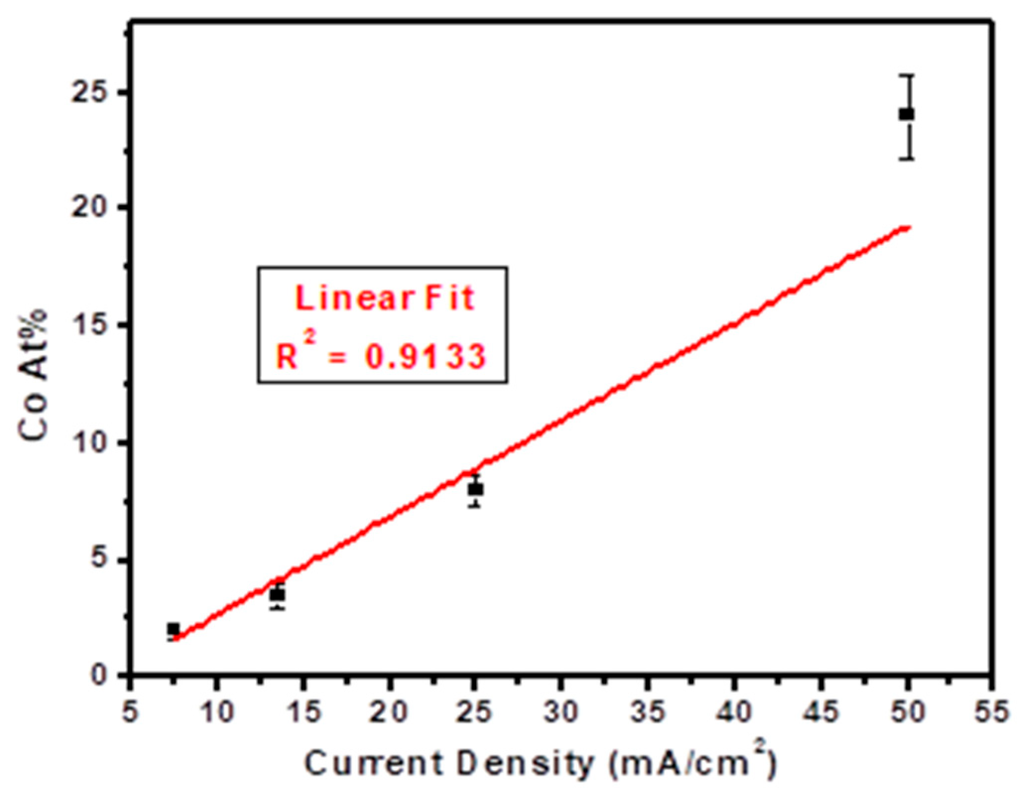
Similar XPS depth profiles of the other films were used to quantify the alloy composition as a function of current density and Co content, including a “zero percent Co” film deposited with the same electrolyte bath with no cobalt salt. The results are plotted in Figure 2 and summarized in Table 1, showing that higher current densities resulted in greater cobalt incorporation in the films. At lower current densities (7.5–13 mA/cm2), Co content increases modestly from 2 at.% to 3.5 at.%, reflecting slower deposition kinetics that favor Cu deposition over Co. At a moderate current density (25 mA/cm2), Co content reaches 7 at.%, while a sharp increase to 24 at.% is observed at the highest current density (50 mA/cm2), driven by higher overpotentials that promote Co deposition. A linear fit to the data has been added as a red line in Figure 2, making clear the non-linear response to current density, which may enable tailoring Co incorporation and optimizing alloy compositions for specific applications, without modifying the electrolyte composition.
To focus the remainder of the study, films with Co compositions of 2 at.%, and 24 at.% were utilized to examine the microstructure and solute distribution in the Cu(Co) alloy films.

3.2. Microstructure Analysis

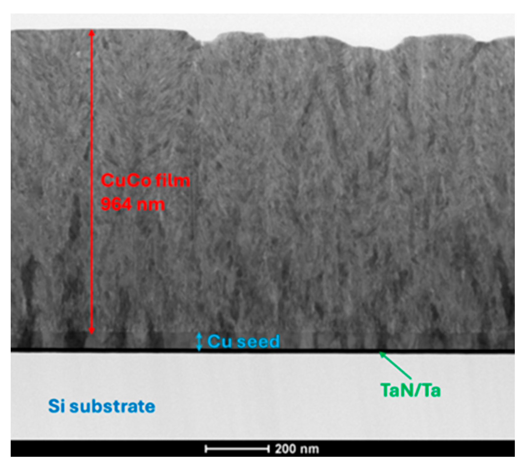
Figure 3 presents a low magnification BF-STEM image of the cross-section of a Cu(Co) film containing 2% Co. The measured film thickness in this case was 964 nm, which is close to the target thickness of 1 µm. The film thickness was generally homogeneous across the sample area, with variations less than 10% as can be seen in Figure 3. This was deemed an acceptable variation for subsequent indentation and electrical measurements. The cross-sectional image also reveals a distinct interface between the Cu seed layer and the deposited CuCo alloy film. The alloys film consists of small grains across the entire film thickness, with an average size of approximately 18 nm. Little to no self-annealing is observed, in contrast with typical electroplated copper films, which undergo dramatic grain growth after deposition. This lack of grain growth in these alloys, even after 1 week at room temperature, is attributed to the presence of trisodium citrate incorporated from the deposition bath, which effectively inhibits grain growth in copper [32].
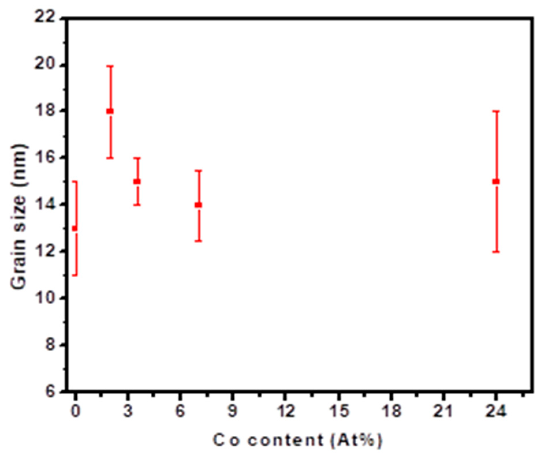
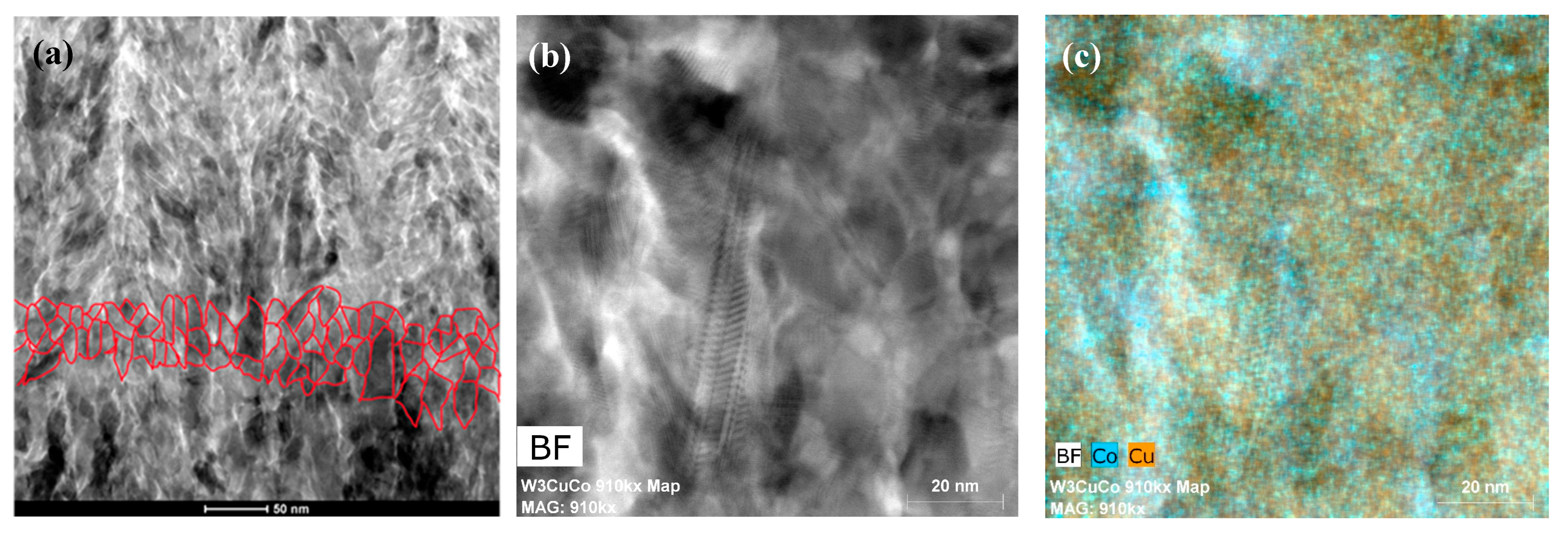
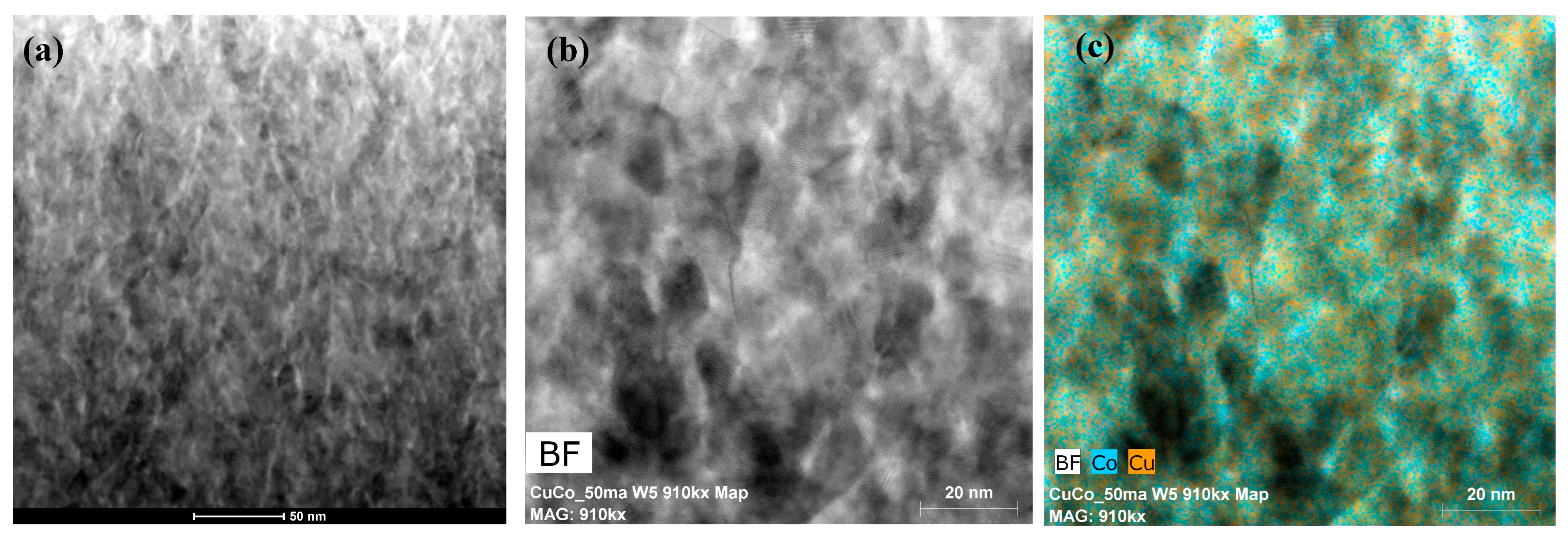
The grain size of the alloy films was determined systematically using the linear intercept, and the results are plotted against Co content in Figure 4. The measurements were obtained from BF-STEM images, with a representative example shown in Figure 5a (outlined grains). More than 200 grains were analyzed across different locations to ensure statistical reliability. The analysis reveals that the Co content does not significantly influence grain size, as the variations across all tested Co compositions were negligible and fell within the margin of error. The grain size of all Cu(Co) alloy films (including 0% Co) was found to fall between 10 and 20 nm, as shown in representative images in Figure 5a and Figure 6a for the 2% and 24% Co films. Higher magnification BF-STEM images of these films are shown in Figure 5b,c for clarity. These results suggest that the cobalt content does not have a measurable effect on the grain size of Cu(Co) films under the studied conditions. Instead, the findings indicate that the grain size is primarily governed by the deposition chemistry and process parameters, with trisodium citrate rather than the cobalt itself playing a critical role in preserving the very fine as-deposited microstructure and inhibiting grain growth.
STEM-EDS was used to map the Co distribution in these films, shown in Figure 5c and Figure 6c as overlays on the BF-STEM images from Figure 5b and Figure 6b. In these maps, cobalt is seen segregating to grain boundaries throughout the entire film thickness for both samples, but no evidence of small three-dimensional precipitates was observed within the Cu(Co) films.
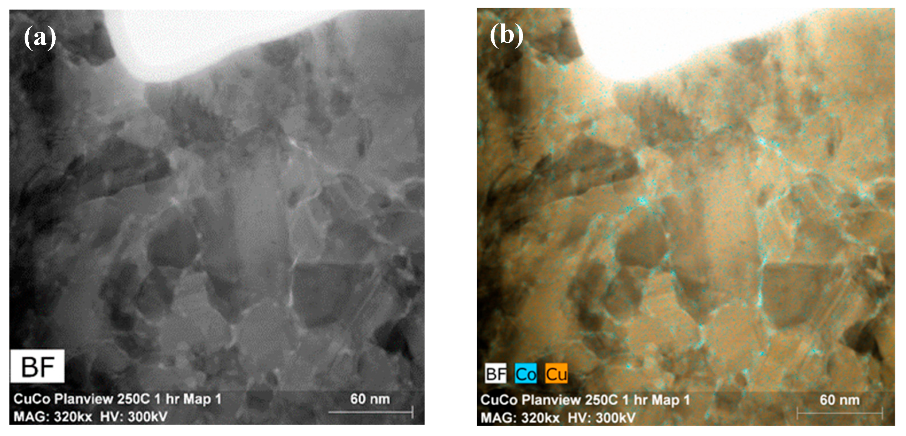
Since small grain size results in high resistance, the films were annealed to encourage grain growth. Figure 7 shows the microstructure of a 2 at.% Co sample which was annealed at 250 °C for 1 h. This temperature was selected to enable grain growth and microstructural evolution while minimizing interdiffusion or phase transformations, in alignment with thermal budgets typically used in back-end-of-line (BEOL) semiconductor processing. The grain size is ~70 nm, a moderate increase from its as-deposited value of 18 nm. Figure 7b overlays the corresponding EDS map on the STEM image, showing significant cobalt segregation at the grain boundaries and triple points, as expected from reports in the literature [23]. Due to its low solubility in Cu, Co precipitates during heating, with grain boundaries facilitating the necessary diffusion [33,34]. Initially, Co precipitation enables grain growth of the copper matrix, but as Co particles increase in size, they pin the grain boundaries and dislocations, restricting further grain growth [35]. This pinning also increases the temperature at which the material can undergo stress relaxation, since higher temperatures are needed to allow dislocations or other defects to move in response to stress. In the case of the Cu–Co alloys, the increase in stress relaxation temperature means that the material will be more resistant to plastic deformation (i.e., the ability to permanently deform under stress) at the bonding temperature. Having a material which is more stable and less likely to deform under stress is beneficial for the long-term performance of such alloys in electronic and semiconductor applications.

3.3. Mechanical Properties: Hardness and Modulus

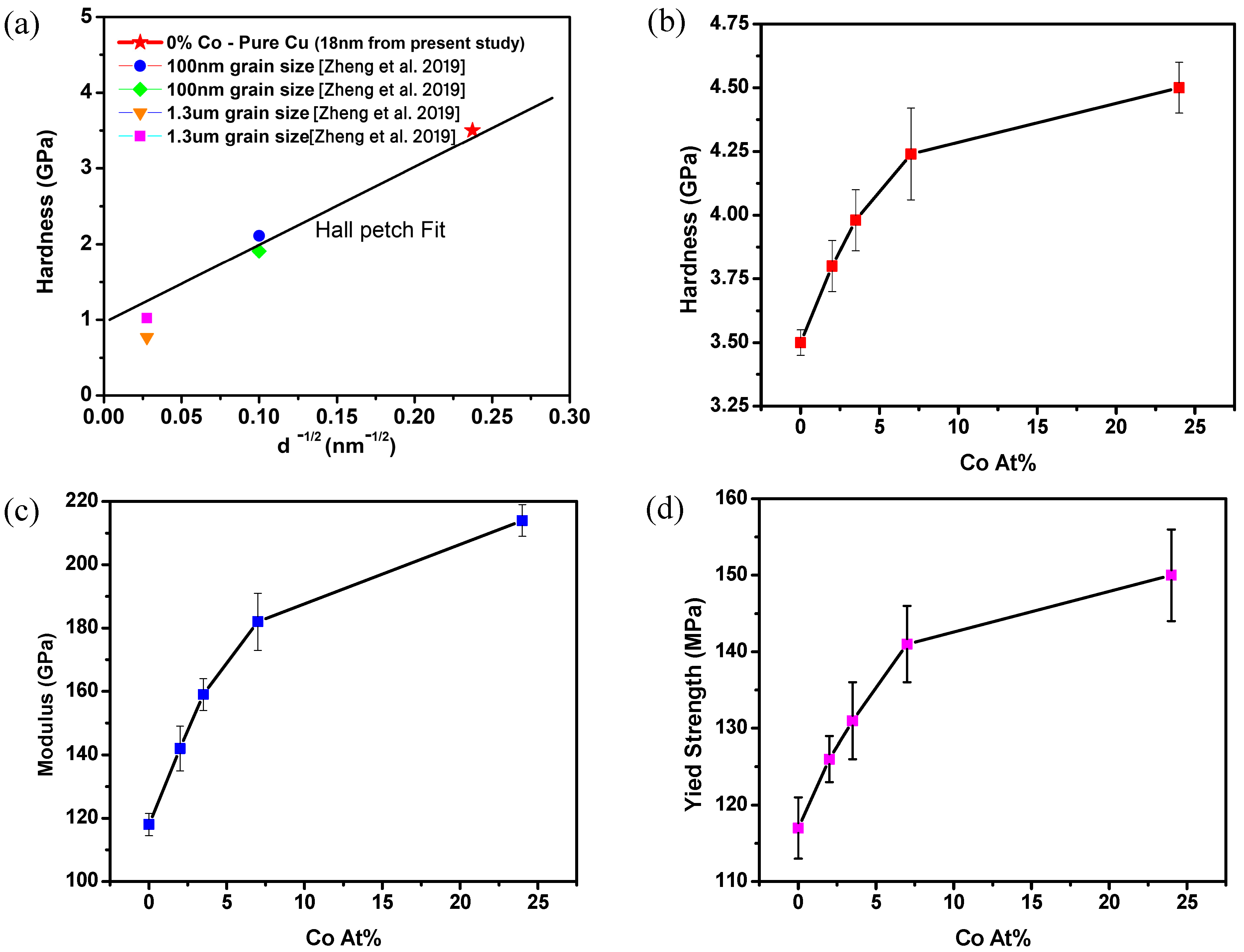
Nanoindentation measurements were performed to determine the hardness and modulus values of Cu(Co) alloy films, plotted in Figure 8. A zero percent Co film was used as a baseline to evaluate the impact of Co addition on hardness and modulus, while maintaining a similar microstructure governed by the incorporation of citrate from the electroplating bath. The hardness of this 0% Co film is compared to values from the literature [36] in Figure 8a and falls along the extrapolated Hall–Petch relationship (added to the figure as a guide to the eye). This empirical relationship describes the dependence of hardness (H) on grain size (d) according to:
H = H0 + k·d−1/2
where H is hardness and d the average grain size. H0 represents the intrinsic hardness of the material and k is a material-specific strength coefficient. According to this relationship, as the grain size (d) decreases, the term d−1/2 increases, leading to an increase in hardness (H) [37]. The 0% Co film in this study is ultrafine but still falls on the straight-line extrapolation from the literature data. Nevertheless, it is important to note that the Hall–Petch relationship exclusively addresses the grain size’s impact on hardness and does not account for other influencing factors such as material impurities and other defects. It is worth noting that the hardness and modulus values obtained in this study for 0% Co film are in reasonable agreement with the literature data for nanocrystalline copper. For example, the literature reports a hardness of ~3.2 GPa and a Young’s modulus of ~108 GPa for Cu films with a grain size of 25 nm [38,39]. Some variation from these values is justified due to differences in experimental methodology, actual grain size, and film quality.
Because all of the films in this study had a similar ultrafine structure, it might be expected that all films exhibited a similar hardness. However, Figure 8b shows the hardness of the films increased non-linearly with cobalt content, and Figure 8c shows a similar trend for the modulus. These values are also reported in Table 2. The observed rise in hardness and modulus can be attributed to impurity strengthening, i.e., Co atoms impeding dislocation movement, which is the primary mechanism of deformation in metals [40,41].
The strengthening mechanisms in Cu–Co alloys evolve with increasing cobalt content, transitioning from solid solution strengthening to precipitation hardening. At low cobalt concentrations, cobalt atoms dissolve into the copper matrix, forming a substitutional solid solution. This behavior is consistent with the Co–Cu binary phase diagram, which indicates the limited solubility of cobalt in copper. The system is characterized by a miscibility gap in the solid state—a widely known feature of the Cu–Co system—indicating that Co and Cu tend to separate into Co-rich and Cu-rich phases rather than forming extensive solid solutions at higher concentrations [42,43]. The size mismatch between Co and Cu atoms introduces lattice distortions that impede dislocation motion and enhance yield strength. This solid solution strengthening effect is proportional to the Co concentration within the solubility limit. As Co content increases beyond this solubility limit, excess cobalt precipitates out of the supersaturated solid solution, forming Co-rich particles within the Cu matrix. These precipitates obstruct dislocation movement through mechanisms such as the Orowan bypass, where dislocations loop around the particles, leading to increased strength [41,44]. The size, distribution, and coherency of these precipitates significantly influence the extent of strengthening. Additionally, at certain compositions and thermal treatments, spinodal decomposition may occur, causing a fine-scale, continuous modulation of composition within grains. This introduces internal stress fields that further hinder dislocation motion, contributing to the overall strengthening of the alloy [45,46].
Furthermore, the yield strength values for Cu(Co) films were calculated using Tabor’s relationship (σy ≈ HV/3, where HV is the Vickers hardness and σy is the yield strength) [47]. To estimate σy, nanoindentation measurements were performed using a Berkovich indenter, and hardness values were extracted using the Oliver–Pharr method. These values are reported in GPa, which is standard for instrumented nanoindentation. However, since the empirical Tabor relation is conventionally applied to hardness values in Vickers (HV), a conversion step was required. As a commonly used approximation, hardness values in GPa were converted to HV (using the relation: 1 GPa ≈ 100 HV). This conversion enabled the application of the Tabor relation: σy ≈ HV/3; which implies σy is the yield strength of the material in MPa.
For example, in the case of sample 1 from Table 2, with a nanoindentation hardness of 3.5 GPa, it corresponds to approximately 350 HV, resulting in an estimated σy of ~117 MPa. This value is in good agreement with previously reported data for nanocrystalline Cu; for instance, Lu et al. reported a yield strength of 119 MPa for electrodeposited Cu with a larger grain size of 27 nm [48]. The slight difference in yield strength, despite the smaller grain size in this study, may be attributed to variations in microstructure or impurity content introduced during the electrodeposition process. All reported yield strength values for Cu(Co) alloys in this work were derived using this procedure and plotted as a function of cobalt content, shown in Figure 8d. The increase with cobalt content again reflects the impurity strengthening effect of cobalt, as higher Co concentrations improve the hardness and, consequently, the yield strength of the alloy. Given that all samples in this study possess a similar ultrafine grain structure, the increase cannot be attributed to grain boundary strengthening. Instead, the strengthening is dominated by the evolving microstructure of the Cu–Co alloy, transitioning from solute strengthening at low Co levels to precipitation and spinodal strengthening at higher concentrations. This aligns with existing findings that emphasize the limited role of solid solution strengthening and highlight the critical impact of Co on mechanical performance through precipitation mechanisms [42,43,49].
Since materials with higher yield strength are less likely to deform under the compressive forces applied during bonding, alloying copper with cobalt can help maintain alignment accuracy and prevent defects such as void formation, cracking or delamination. Thus, optimizing the yield strength through alloying, as observed with increasing Co content, can be an effective strategy to enhance the performance and reliability of Cu hybrid bonds.

3.4. CTE Variation with Co Incorporation

Three films (0%, 2% and 24% Co) were analyzed for their CTE using high-temperature X-ray diffraction (HT-XRD). The relative change in lattice parameter (Δa/a0) was plotted against temperature in Figure 9a. From the slope of this data, the CTE was extracted and plotted in Figure 9b. The film with 2% Co content exhibited a modest 7% increase in CTE relative to the baseline material (0% Co), whereas the sample with 24% Co content demonstrated a significant 58% increase. This disproportionate response to the inclusion of Co is encouraging, as it means a relatively modest Co content can still result in substantial CTE gains, offering an opportunity to optimize materials for specific thermal performance requirements.
The situation for constrained geometries, such as the interconnects at a hybrid bonding interface, may have an even more dramatic CTE response. In the present study, the samples were blanket films constrained only by adhesion to the substrate and spanning a relatively large area, such that in-plane expansion was largely unconstrained. By contrast, Cu pads used in hybrid bonding are highly confined by the surrounding dielectric, so thermal expansion occurs primarily in the vertical direction. This geometric constraint generates localized stresses that amplify the apparent out-of-plane expansion relative to blanket films. Consequently, to close a given dishing gap (for example, ~2 nm), a Cu–Co alloy pad embedded in dielectric can achieve the necessary vertical expansion at a lower annealing temperature than pure Cu would require, due to the combined effects of microstructural tuning and constraint. This interpretation is consistent with prior reports on enhanced thermal expansion of nanocrystalline Cu pads under confinement [28,50].
Interestingly, the literature highlights a fascinating interplay between grain size and thermal expansion behavior: fine grains (0.15 µm) exhibit nearly double the CTE of coarse grains (2.5 µm) [50]. In our case, the grain size is even smaller (by a factor of ~10×), and when cobalt (Co) is introduced into the Cu to form an alloy, the resulting combination is anticipated to exhibit significantly greater thermal expansion. However, experimental findings from another IMEC study [51] highlight a critical challenge. Measurements on sub-μm Cu pads show that as pad size decreases further, the CTE significantly diminishes, underscoring the scaling limitations of the classic hybrid bonding approach. Finite Element Method (FEM) simulations also reveal that at sub-μm dimensions, Cu expansion becomes increasingly limited. These findings emphasize the challenges posed by fine-pitch connections, where smaller pad sizes require extraordinary chemical–mechanical polishing (CMP) efforts and demand materials with higher CTE to maintain effective bonding.
Given these considerations, the synergistic effect of ultrafine grains and Cu(Co) alloy behavior presents a promising avenue for optimizing materials in low-temperature hybrid bonding applications, where both grain size and cobalt content can help address the challenges posed by scaling limitations and pad size constraints.

3.5. Electrical Measurements

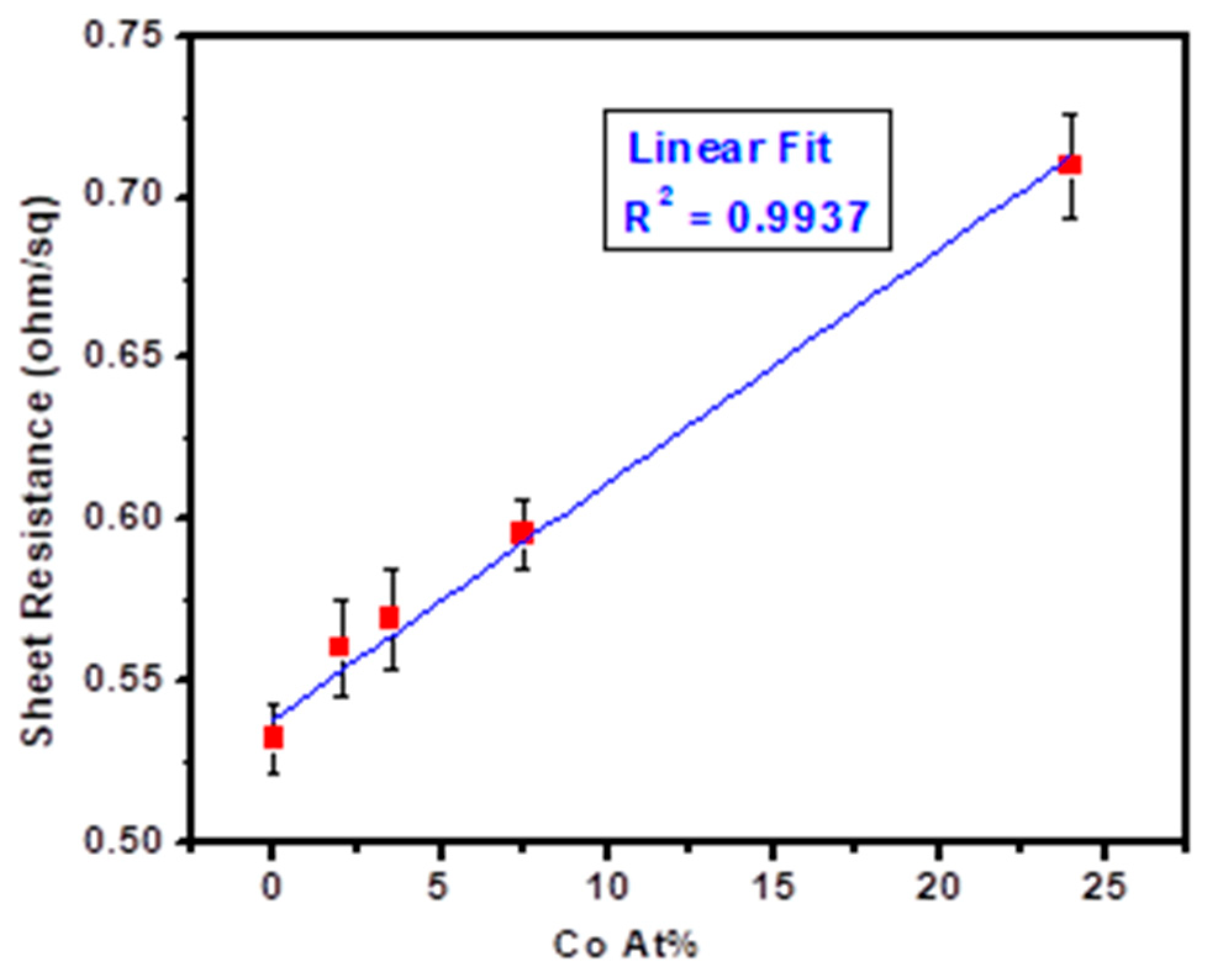
However, the above gains in mechanical behavior come at a cost to electrical behavior. The sheet resistance values of the Cu(Co) alloy films are plotted in Figure 10, showing a gradual increase with increasing cobalt concentration. For fine-grained, 0% Co-copper, the measured sheet resistance is 0.53 Ω/sq—nearly five times higher than the 0.108 Ω/sq reported in the literature [52]. This considerable increase, even in the absence of cobalt, can be attributed to the presence of carbon and oxygen impurities from the citrate additive used and the influence of grain size. In our case, the grain size is comparable to the mean free path of copper (39 nm), and the increase in resistance is unsurprising. As cobalt content increases to 2%, 3.5%, 7.5%, and 24%, the sheet resistance rises to 0.56 Ω/sq, 0.57 Ω/sq, 0.59 Ω/sq, and 0.70 Ω/sq, respectively. This trend indicates that the addition of cobalt, while beneficial for certain mechanical and thermal properties, introduces additional electron scattering sites due to lattice distortions and the presence of solute atoms. These scattering events reduce the mean free path of conduction electrons, thereby increasing resistivity [53]. The increase is relatively modest at low Co concentrations but becomes more pronounced at higher Co concentrations, reflecting the cumulative impact of alloying on electron mobility. While the higher sheet resistance will impact electrical performance, a certain degree can be tolerated as a trade-off for the mechanical and thermal property enhancements achieved with Co doping.
Notably, thickness, which is a critical factor affecting sheet resistance, was consistent across all deposited films, measured within 1 ± 0.05 µm. This minimal variation in thickness ensures a negligible impact on resistance values. Additionally, the grain size remained similar across all samples, with Co content being the only variable. Although substrate effects may contribute to resistance changes, these effects are expected to be consistent due to the uniform thickness across samples.
Accordingly, the observed increase in resistance with higher Co content can be attributed to the cumulative effects of cobalt-induced electron scattering and the consistent structural parameters across the tested samples.
Taken together, the thermal and electrical results reveal the trade-offs that define the practical Co concentration range for interconnect integration. Although the Cu–Co phase diagram shows only limited equilibrium solubility of Co in Cu (<0.2 at.% at ≤400 °C), our results demonstrate that small Co additions (≈2 at.%) already provide a measurable CTE increase (+7%) with only a modest rise in sheet resistance. At higher concentrations (e.g., 24 at.% Co), the CTE enhancement is significant (+58%), but sheet resistance increases linearly with Co content, making such levels unsuitable for interconnect applications. Thus, for hybrid bonding, the practical Co addition must remain in the very dilute regime (≤1–2 at.%), where the trade-off between improved thermal expansion and electrical performance remains acceptable.

4. Conclusions

Cu(Co) alloy films were co-deposited using electrochemical deposition, with alloy composition precisely controlled via current density. Microstructural analysis revealed that cobalt predominantly segregated to grain boundaries, stabilizing the microstructure without forming precipitates within the grains, while the deposition chemistry suppressed grain growth. Annealing amplifies this segregation effect, though precipitation at triple points began. The alloy films exhibit a well-balanced combination of mechanical, thermal, and electrical properties, making them suitable for hybrid bonding applications. Increasing cobalt content enhances hardness, modulus, and yield strength, providing improved resistance to deformation and ensuring structural stability. Thermal expansion, measured via CTE, shows a significant and tunable increase with Co content, which is crucial for enabling low-temperature bonding. Electrical measurements indicate a modest rise in sheet resistance with Co content, attributed to increased electron scattering, which remains a trade-off for the mechanical and thermal property gains. These findings underscore the potential of Cu(Co) alloys as tunable materials, offering a tailored balance of properties for engineering reliable metal interconnections in hybrid bonding applications.

Author Contributions

Conceptualization, K.D.; Methodology, S.S.; Formal analysis, S.S.; Investigation, S.S.; Writing—original draft, S.S.; Writing—review and editing, K.D.; Supervision, K.D.; Project administration, K.D.; Funding acquisition, K.D. All authors have read and agreed to the published version of the manuscript.

Funding

This work was supported in part by the National Science Foundation under the award DMR-1808277.

Institutional Review Board Statement

Not applicable.

Informed Consent Statement

Not applicable.

Data Availability Statement

The original contributions presented in this study are included in the article. Further inquiries can be directed to the corresponding author.

Acknowledgments

The authors gratefully acknowledge the characterization support and facility use, including the NYCREATES Metrology group for the XPS and STEM/EDS, the Center for Materials, Devices, and Integrated Systems at Rensselaer Polytechnic Institute for the nanoindentation testing, and the Institute for Advanced Materials and Manufacturing at the University of Tennessee for assistance with the high-temperature X-ray diffraction.

Conflicts of Interest

The authors declare no conflicts of interest.

References

  1. Hsiung, C.K.; Chen, K.N. A Review on Hybrid Bonding Interconnection and Its Characterization. IEEE Nanotechnol. Mag. 2024, 18, 41–50. [Google Scholar] [CrossRef]
  2. Morrow, P.R.; Park, C.M.; Ramanathan, S.; Kobrinsky, M.J.; Harmes, M. Three-Dimensional Wafer Stacking via Cu-Cu Bonding Integrated with 65-Nm Strained-Si/Low-k CMOS Technology. IEEE Electron Device Lett. 2006, 27, 335–337. [Google Scholar] [CrossRef]
  3. Ko, C.T.; Chen, K.N. Low Temperature Bonding Technology for 3D Integration. Microelectron. Reliab. 2012, 52, 302–311. [Google Scholar] [CrossRef]
  4. Zhang, S.; Li, Z.; Zhou, H.; Li, R.; Wang, S.; Paik, K.W.; He, P. Challenges and Recent Prospectives of 3D Heterogeneous Integration. In E-Prime—Advances in Electrical Engineering, Electronics and Energy; Elsevier Ltd.: Amsterdam, The Netherlands, 2022. [Google Scholar] [CrossRef]
  5. Le, X.B.; Choa, S.H. Assessment of the Risk of Crack Formation at a Hybrid Bonding Interface Using Numerical Analysis. Micromachines 2024, 15, 1332. [Google Scholar] [CrossRef] [PubMed]
  6. Beilliard, Y.; Estevez, R.; Parry, G.; McGarry, P.; Di Cioccio, L.; Coudrain, P. Thermomechanical Finite Element Modeling of Cu–SiO2 Direct Hybrid Bonding with a Dishing Effect on Cu Surfaces. Int. J. Solids Struct. 2017, 117, 208–220. [Google Scholar] [CrossRef]
  7. Panchenko, I.; Wenzel, L.; Mueller, M.; Rudolph, C.; Hanisch, A.; Wolf, J.M. Microstructure Development of Cu/SiO Hybrid Bond Interconnects After Reliability Tests. IEEE Trans. Compon. Packag. Manuf. Technol. 2022, 12, 410–421. [Google Scholar] [CrossRef]
  8. Singh, S.; Dunn, K. Composition-Tunable Properties of Cu(Ag) Alloy for Hybrid Bonding Applications. Materials 2023, 16, 7481. [Google Scholar] [CrossRef]
  9. Dag, S.; Liu, M.; Jiang, L.; Kiaee, A.; See, G.; Lianto, P.; Ayyagari-Sangamalli, B.; Bazizi, E.M. Development of Copper Thermal Coefficient For Low Temperature Hybrid Bonding. In Proceedings of the Electronic Components and Technology Conference, Orlando, FL, USA, 30 May–2 June 2023; Institute of Electrical and Electronics Engineers Inc.: New York, NY, USA, 2023; Volume 2023, pp. 342–349. [Google Scholar] [CrossRef]
  10. Mirkarimi, L.; Uzoh, C.; Suwito, D.; Lee, B.; Fountain, G.; Workman, T.; Theil, J.; Gao, G.; Buckalew, B.; Oberst, J.; et al. The Influence of Cu Microstructure on Thermal Budget in Hybrid Bonding. In Proceedings of the Electronic Components and Technology Conference, San Diego, CA, USA, 31 May–3 June 2022; Institute of Electrical and Electronics Engineers Inc.: New York, NY, USA, 2022; pp. 162–167. [Google Scholar] [CrossRef]
  11. Sachs, E.; Cima, M.; Cornie, J.; Brancazio, D.; Bredt, J.; Curodeau, A.; Fan, T.; Khanuja, S.; Lauder, A.; Lee, J.; et al. Three dimensional Printing: The Physics and Implications of Additive Manufacturing. CIRP Ann. 1993, 42, 257–260. [Google Scholar] [CrossRef]
  12. Ganesh, K.J.; Darbal, A.D.; Rajasekhara, S.; Rohrer, G.S.; Barmak, K.; Ferreira, P.J. Effect of Downscaling Nano-Copper Interconnects on the Microstructure Revealed by High Resolution TEM-Orientation-Mapping. Nanotechnology 2012, 23, 135702. [Google Scholar] [CrossRef]
  13. Pu, W.; He, X.; Ren, J.; Wan, C.; Jiang, C. Electrodeposition of Sn-Cu Alloy Anodes for Lithium Batteries. Electrochim. Acta 2005, 50, 4140–4145. [Google Scholar] [CrossRef]
  14. Ivanova, A.R.; Nuesca, G.; Chen, X.; Goldberg, C.; Kaloyeros, A.E.; Arkles, B.; Sullivan, J.J. The Effects of Processing Parameters in the Chemical Vapor Deposition of Cobalt from Cobalt Tricarbonyl Nitrosyl. J. Electrochem. Soc. 1999, 146, 2139. [Google Scholar] [CrossRef]
  15. Kaloyeros, A.E. Method of Interlayer Mediated Epitaxy of Cobalt Silicide from Low Temperature Chemical Vapor Deposition of Cobalt. U.S. Patent US6346477B1, 12 February 2002. [Google Scholar]
  16. Lane, M.W.; Liniger, E.G.; Lloyd, J.R. Relationship between Interfacial Adhesion and Electromigration in Cu Metallization. J. Appl. Phys. 2003, 93, 1417–1421. [Google Scholar] [CrossRef]
  17. Zhang, L.; Zhou, J.P.; Im, J.; Ho, P.S.; Aubel, O.; Hennesthal, C.; Zschech, E. Effects of Cap Layer and Grain Structure on Electromigration Reliability of Cu/Low-k Interconnects for 45 Nm Technology Node. In Proceedings of the 2010 IEEE International Reliability Physics Symposium, Anaheim, CA, USA, 2–6 May 2010; IEEE: New York, NY, USA, 2010; pp. 581–585. [Google Scholar] [CrossRef]
  18. Zhang, L.; Kraatz, M.; Aubel, O.; Hennesthal, C.; Zschech, E.; Ho, P.S. Grain Size and Cap Layer Effects on Electromigration Reliability of Cu Interconnects: Experiments and Simulation. In Proceedings of the AIP Conference Proceedings, Annapolis, MD, USA, 1–4 November 2010; Volume 1300, pp. 3–11. [Google Scholar] [CrossRef]
  19. Arnaud, L.; Lamontagne, P.; Bana, F.; Le Friec, Y.; Waltz, P. Study of Electromigration Void Nucleation Time in Cu Interconnects with Doping Elements. Microelectron. Eng. 2013, 107, 145–150. [Google Scholar] [CrossRef]
  20. Rosenberg, R.; Batson, P.E.; Bruley, J.; Splinter, S.J.; Muller, D.A. Observations on the Influence of Solute on Grain Boundary Diffusion and Electromigration; AIP Publishing: Melville, NY, USA, 2009; pp. 127–134. [Google Scholar] [CrossRef]
  21. Barmak, K.; Gungor, A.; Rollett, A.D.; Cabral, C.; Harper, J.M.E. Texture of Cu and Dilute Binary Cu-Alloy Films: Impact of Annealing and Solute Content. Mater. Sci. Semicond. Process. 2003, 6, 175–184. [Google Scholar] [CrossRef]
  22. Barmak, K.; Gungor, A.; Cabral, C.; Harper, J.M.E. Annealing Behavior of Cu and Dilute Cu-Alloy Films: Precipitation, Grain Growth, and Resistivity. J. Appl. Phys. 2003, 94, 1605–1616. [Google Scholar] [CrossRef]
  23. Harper, J.M.E.; Gupta, J.; Smith, D.A.; Chang, J.W.; Holloway, K.L.; Cabral, C.; Tracy, D.P.; Knorr, D.B. Crystallographic Texture Change during Abnormal Grain Growth in Cu-Co Thin Films. Appl. Phys. Lett. 1994, 65, 177–179. [Google Scholar] [CrossRef]
  24. Gupta, D. Diffusion Processes in Advanced Technological Materials; Gupta, D., Ed.; Springer: Berlin/Heidelberg, Germany, 2005. [Google Scholar] [CrossRef]
  25. Cantwell, P.R.; Tang, M.; Dillon, S.J.; Luo, J.; Rohrer, G.S.; Harmer, M.P. Grain Boundary Complexions. Acta Mater. 2014, 62, 1–48. [Google Scholar] [CrossRef]
  26. Gungor, A.; Barmak, K.; Rollett, A.D.; Cabral, C.; Harper, J.M.E. Texture and Resistivity of Dilute Binary Cu(Al), Cu(In), Cu(Ti), Cu(Nb), Cu(Ir), and Cu(W) Allow Thin Films. J. Vac. Sci. Technol. B Microelectron. Nanometer Struct. 2002, 20, 2314–2319. [Google Scholar] [CrossRef]
  27. Zhang, S.-L.; Harper, J.M.E.; Cabral, C.; D’heurle, F.M. In Situ Resistivity Study of Copper-Cobalt Films: Precipitation, Dissolution and Phase Transformation. Thin Solid Film. 2001, 401, 298–305. [Google Scholar] [CrossRef]
  28. De Messemaeker, J.; Witters, L.; Zhang, B.; Tsau, Y.W.; Fodor, F.; De Vos, J.; Beyer, G.; Croes, K.; Beyne, E. New Cu “Bulge-Out” Mechanism Supporting SubMicron Scaling of Hybrid Wafer-to-Wafer Bonding. In Proceedings of the Electronic Components and Technology Conference, Orlando, FL, USA, 30 May–2 June 2023; Institute of Electrical and Electronics Engineers Inc.: New York, NY, USA, 2023; Volume 2023, pp. 109–113. [Google Scholar] [CrossRef]
  29. Joi, A.; Akolkar, R.; Landau, U. Pulse Electrodeposition of Copper-Manganese Alloy for Application in Interconnect Metallization. J. Electrochem. Soc. 2013, 160, D3145–D3148. [Google Scholar] [CrossRef]
  30. Paunovic, M.; Schlesinger, M.; Synder, D. Modern Electroplating; Schlesinger, M., Paunovic, M., Eds.; John Wiley & Sons: Hoboken, NJ, USA, 2010. [Google Scholar] [CrossRef]
  31. O’Brien, B. The Impact of Seed Layer Structure on the Recrystallization of ECD Cu and Its Alloys. Ph.D. Thesis, University At Albany, State University of New York, Albany, NY, USA, 2015. [Google Scholar]
  32. Singh, S.; Dunn, K. Tuning of Copper Grain Sizes for Integration in Hybrid Bonding Applications. In Proceedings of the 2024 IEEE 10th Electronics System-Integration Technology Conference, ESTC 2024—Proceedings, Berlin, Germany, 11–13 September 2024; Institute of Electrical and Electronics Engineers Inc.: New York, NY, USA, 2024. [Google Scholar] [CrossRef]
  33. Haessner, F. (Ed.) Recrystallization of Metallic Materials, 2nd ed.; Riederer-Verlag: Stuttgart, Germany, 1978. [Google Scholar]
  34. Massalski, T.B.; Murray, J.L.; Baker, H.; Bennett, L.H. (Eds.) Binary Alloy Phase Diagrams, 2nd ed.; ASM International: Materials Park, OH, USA, 1990. [Google Scholar]
  35. Ashby, M.F.; Harper, J.; Lewis, J. The Interaction of Crystal Boundaries with Second-Phase Particles. Transactions of the American Institute of Mining, Metallurgical and Petroleum Engineers. Metall. Soc. 1969, 245, 413–420. [Google Scholar]
  36. Zheng, Z.; Chiang, P.C.; Huang, Y.T.; Wang, W.T.; Li, P.C.; Tsai, Y.H.; Chen, C.M.; Feng, S.P. Study of Grain Size Effect of Cu Metallization on Interfacial Microstructures of Solder Joints. Microelectron. Reliab. 2019, 99, 44–51. [Google Scholar] [CrossRef]
  37. Hakamada, M.; Nakamoto, Y.; Matsumoto, H.; Iwasaki, H.; Chen, Y.; Kusuda, H.; Mabuchi, M. Relationship between Hardness and Grain Size in Electrodeposited Copper Films. Mater. Sci. Eng. A 2007, 457, 120–126. [Google Scholar] [CrossRef]
  38. Sanders, P.G.; Eastman, J.A.; Weertman, J.R. Tensile Behavior of Nanocrystalline Copper. 1995. Available online: https://digital.library.unt.edu/ark:/67531/metadc668453/ (accessed on 5 June 2025).[Green Version]
  39. Sun, X.; Reglero, R.; Sun, X.; Yacaman, M.J. Microhardness of Bulk and Higher Density Nanocrystalline Copper Obtained by Hot Compaction. Mater. Chem. Phys. 2000, 63, 82–87. [Google Scholar] [CrossRef]
  40. Sui, F.; Sandström, R. Creep Strength Contribution Due to Precipitation Hardening in Copper–Cobalt Alloys. J. Mater. Sci. 2019, 54, 1819–1830. [Google Scholar] [CrossRef]
  41. Bachmaier, A.; Rathmayr, G.B.; Schmauch, J.; Schell, N.; Stark, A.; De Jonge, N.; Pippan, R. High Strength Nanocrystalline Cu-Co Alloys with High Tensile Ductility. J. Mater. Res. 2019, 34, 58–68. [Google Scholar] [CrossRef]
  42. Bachmaier, A.; Pfaff, M.; Stolpe, M.; Aboulfadl, H.; Motz, C. Phase Separation of a Supersaturated Nanocrystalline Cu-Co Alloy and Its Influence on Thermal Stability. Acta Mater. 2015, 96, 269–283. [Google Scholar] [CrossRef]
  43. Shen, T.D.; Koch, C.C. Formation, Solid Solution Hardening and Softening of Nanocrystalline Solid Solutions Prepared by Mechanical Attrition. Acta Mater. 1996, 44, 753–761. [Google Scholar] [CrossRef]
  44. Dieter, G.E. Mechanical Metallurgy, 3rd ed.; Mc Graw-Hill Book Co.: New York, NY, USA, 1988. [Google Scholar][Green Version]
  45. Katot, M.; Moris, T.; Schwartz, L.H. Hardening by Spinodal Modulated Structure. Acta Metall. 1980, 28, 285–290. [Google Scholar] [CrossRef]
  46. Zhou, X.; Darvishi Kamachali, R.; Boyce, B.L.; Clark, B.G.; Raabe, D.; Thompson, G.B. Spinodal Decomposition in Nanocrystalline Alloys. Acta Mater. 2021, 215, 117054. [Google Scholar] [CrossRef]
  47. Tabor, D. The physical meaning of indentation and scratch hardness. Br. J. Appl. Phys. 1956, 7, 159–166. [Google Scholar] [CrossRef]
  48. Lu, L.; Wang, L.B.; Ding, B.Z.; Lu, K. High-Tensile Ductility in Nanocrystalline Copper. J. Mater. Res. 2000, 15, 270–273. [Google Scholar] [CrossRef]
  49. Butt, M.Z.; Feltham, P. Solid-Solution Hardening. J. Mater. Sci. 1993, 28, 2557–2576. [Google Scholar] [CrossRef]
  50. Lin, H.E.; Tran, D.P.; Chiu, W.L.; Chang, H.H.; Chen, C. Enhanced Thermal Expansion with Nanocrystalline Cu in SiO2 Vias for Hybrid Bonding. Appl. Surf. Sci. 2024, 672, 160784. [Google Scholar] [CrossRef]
  51. Beyne, E.; Kim, S.-W.; Peng, L.; Heylen, N.; De Messemaeker, J.; Okudur, O.O.; Phommahaxay, A.; Kim, T.-G.; Stucchi, M.; Velenis, D.; et al. Scalable, Sub 2 μm Pitch, Cu/SiCN to Cu/SiCN Hybrid Wafer-to-Wafer Bonding Technology. In Proceedings of the 2017 IEEE International Electron Devices Meeting (IEDM), San Francisco, CA, USA, 2–6 December 2017; IEEE: New York, NY, USA, 2017; pp. 32.4.1–32.4.4. [Google Scholar] [CrossRef]
  52. Huang, Q. Effects of Impurity Elements on Isothermal Grain Growth of Electroplated Copper. J. Electrochem. Soc. 2018, 165, D251–D257. [Google Scholar] [CrossRef]
  53. Gall, D. Electron Mean Free Path in Elemental Metals. J. Appl. Phys. 2016, 119, 085101. [Google Scholar] [CrossRef]
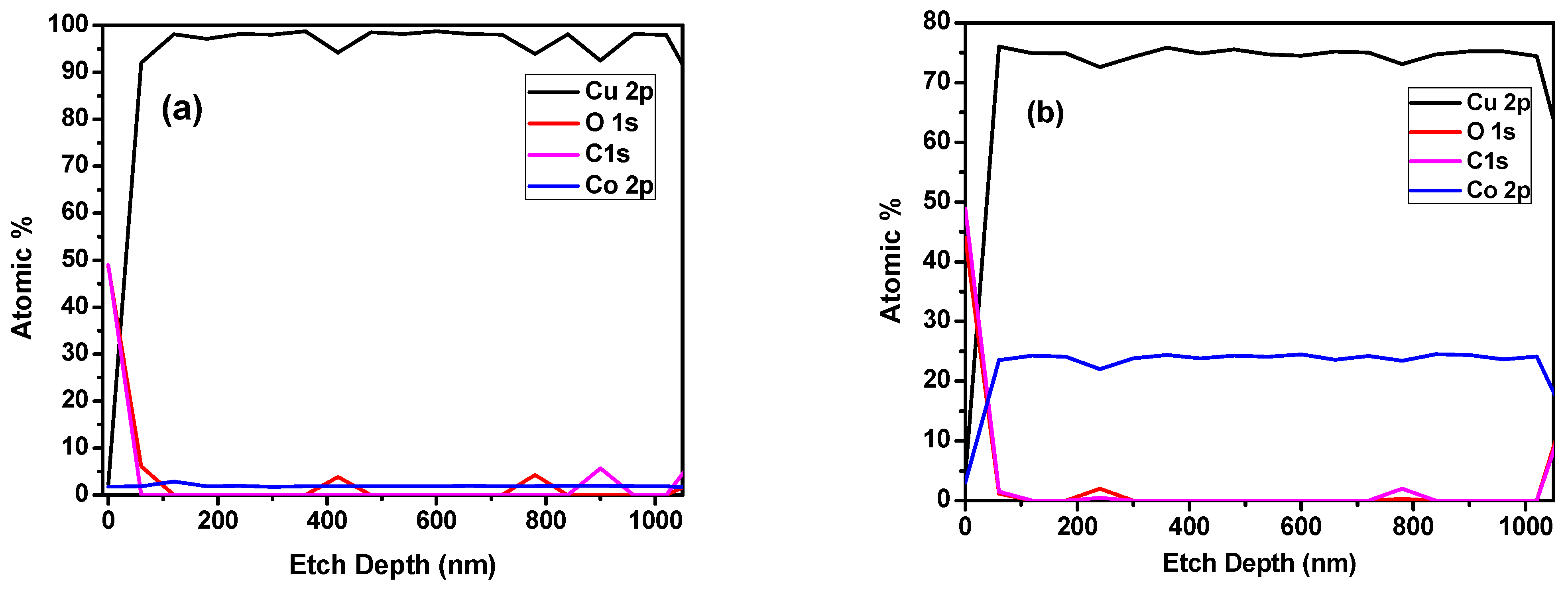
Figure 1. Quantified XPS depth profiles for a Cu(Co) film deposited using a current density of (a) 7.5 mA/cm2 and (b) 50 mA/cm2. The x-axis shows the etch depth in nm, whereas the y-axis shows the corresponding atomic composition for various elements such as Cu, Co, O, and C.
Metals 15 01023 g001
Figure 2. Co content vs. current density for CuCo alloy films deposited using the citrate deposition method. As anticipated, Co content increases in alloy films with increase in current density. For all films except the ‘zero cobalt reference’, the composition of the electrolyte (including cobalt salt concentration) was held constant.
Metals 15 01023 g002
Figure 3. Low magnification BF-STEM image of the cross-section of an as-deposited Cu(Co) alloy film with 2% Co content. The cross section shows the fine grain microstructure of the deposited film with a thickness close to the target thickness of 1 µm.
Metals 15 01023 g003
Figure 4. Grain size vs. Co content of alloy films, showing all films have a similar microstructure, with grains in the range of 10 to 20 nm.
Metals 15 01023 g004
Figure 5. Microstructure of an as-deposited 2% Co alloy film. (a) Lower magnification BF-STEM image of cross section, revealing an average grain size of 18 nm, with outlined grains shown for reference to illustrate the grain size analysis method. (b) High magnification BF-STEM image. (c) EDS map overlaid on the higher magnification BF-STEM image, showing Co segregation to grain boundaries.
Metals 15 01023 g005
Figure 6. Microstructure of an as-deposited 24% Co alloy film. (a) Lower magnification BF-STEM image of cross section, revealing an average grain size of 15 nm. (b) High magnification BF-STEM image. (c) EDS map overlaid on the higher magnification BF-STEM image, showing Co segregation to grain boundaries.
Metals 15 01023 g006
Figure 7. Microstructure of a 2% Co alloy film after annealing for 1 h at 250 °C. (a) Plan-view BF-STEM image showing moderate grain growth has occurred, resulting in a grain size of ~70 nm. (b) EDS map overlaid on the BF-STEM image, showing significant Co segregation to grain boundaries and triple points, resulting in the formation of precipitates not seen in the as-deposited films.
Metals 15 01023 g007
Figure 8. Mechanical properties of Cu(Co) alloys. (a) Hardness of copper with no cobalt, as a function of grain size. Stars represent this study, with grain-size dependent data adapted from ref. [36] for comparison. A straight line representing the empirical Hall–Petch relation is included as a guide for the eye. (b) Hardness vs. Co content of the Cu(Co) alloy films in this study, showing the hardness values increasing nonlinearly as the Co content was increased, despite a similar grain size to the 0% Co film. (c) Modulus of Cu(Co) alloy films, showing the values increase with the increase in the Co content of the films. (d) Calculated yield strength of the Cu(Co) alloy films showing the yield strength increasing with the increasing Co content of the films.
Metals 15 01023 g008
Figure 9. Coefficient of thermal expansion. (a) Temperature dependence fractional change in the lattice parameter as a function of temperature for three of the films in this study. (b) CTE calculated for the 0% Co films along with the three films shown in (a).
Metals 15 01023 g009
Figure 10. Sheet resistance vs. the Co content of Cu(Co) films showing that with an increase in the Co content of the Cu(Co) films, the sheet resistance also increases linearly.
Metals 15 01023 g010
Table 1. Current density used for CuCo alloy deposition and respective Co content. For all films except the ‘zero cobalt reference’, the composition of the electrolyte (including cobalt salt concentration) was held constant.
Film NumberCurrent Density (mA/cm2)Co at.%
17.50
27.52
3133.5
4257
55024
Table 2. Hardness, modulus and calculated yield strength values of the films in this study, as a function of Co content in the alloy.
S. No.Co Content (%)Hardness (H) [GPa]Modulus [GPa]Calculated Yield Strength (τyield) [MPa]
103.5118117
223.8142126
33.53.95159131
474.24183141
5244.5214150
Disclaimer/Publisher’s Note: The statements, opinions and data contained in all publications are solely those of the individual author(s) and contributor(s) and not of MDPI and/or the editor(s). MDPI and/or the editor(s) disclaim responsibility for any injury to people or property resulting from any ideas, methods, instructions or products referred to in the content.