Article

Characterization of Different Types of Screen-Printed Carbon Electrodes Modified Electrochemically by Ceria Coatings

1
“Rostislaw Kaischew” Institute of Physical Chemistry, Bulgarian Academy of Sciences, “Acad. G. Bonchev” Street, bl. 11, 1113 Sofia, Bulgaria
2
Institute of General and Inorganic Chemistry, Bulgarian Academy of Sciences, “Acad. G. Bonchev” Street, bl. 11, 1113 Sofia, Bulgaria
*
Author to whom correspondence should be addressed.
Metals 2025, 15(7), 741; https://doi.org/10.3390/met15070741
Submission received: 21 May 2025 / Revised: 25 June 2025 / Accepted: 27 June 2025 / Published: 30 June 2025

Abstract

Electrochemical formation of ceria (mixed Ce2O3 and CeO2) coatings on different types of screen-printed carbon electrodes (SPCEs) (based on graphite (C110), carbon nanotubes (CNT), single-walled carbon nanotubes (SWCNT), carbon nanofibers (CNF), and mesoporous carbon (MC)) were studied. Their potential applications as catalysts for various redox reactions and electrochemical sensors were investigated. The ceria oxide layers were electrodeposited on SPCEs at various current densities and deposition time. The morphology, structure, and chemical composition in the bulk of the ceria layers were studied by SEM and EDS methods. XRD was used to identify the formed phases. The concentration, chemical composition and chemical state of the elements on the surface of studied samples were characterized by XPS. It was established that the increase of the concentration of CeCl3 in the solution and the cathode current density strongly affected the surface structure and concentration (relation between Ce3+ and Ce4+, respectively) in the formed ceria layers. At low concentration of CeCl3 (0.1M) and low values of cathode current density (0.5 mA·cm−2), porous samples were obtained, while with their increase, the ceria coatings grew denser.

1. Introduction

The creation of screen-printed carbon electrodes (SPCEs) led to the essential improvement and expansion of their capabilities as highly sensitive electrochemical sensor (based on measuring various electrical signals—current, potential, or resistance) three-electrode cells used for electro-analytical purposes. This achievement led to the fact that SPCEs form the basis of a significant part of modern stationary and portable analytical sensor systems operating on the principle of three-electrode cells. Among the most widely used substrate materials in the production of SPCEs are graphite (C110), carbon nanotubes (CNT), carbon nanofibers (CNF), mesoporous carbon (MC), and graphene. The different carbon structures vary in shape, size, porosity, and properties: graphite has a layered structure with good electrical conductivity, CNTs and SWCNTs are cylindrical nanotubes with exceptional strength and conductivity, while CNFs are fibers with lower conductivity but good mechanical stability, and mesoporous carbon (MC) has a high surface area and porosity. The advantages of these carrier materials are related to their highly developed effective working surface, a wide range of potentials in which parallel parasitic electrochemical reactions (typical for aqueous solutions) are not observed, high electrical conductivity, due to their electronic structure, and relatively low price.
Single-use electrochemical sensors (designed on the basis of SPCEs), applied in the determination of traces of pollutants and/or toxic substances in environmental and biological samples, are also attractive from the point of view of SPCE design. They can be modified in terms of the requirements for specific analytes. Moreover, the chemical composition and surface structure of the SPCEs can be easily changed, thanks to which more efficient solutions can be implemented in terms of the objects under study. In this regard, in recent years, interest in the development and application of more sensitive, specific, fast, and precise analysis methods using screen-printed electrodes has been growing substantially [1,2]. SPCEs allow implementation of a large number of experiments using small amounts of consumables (samples and reagents) that do not require pre-treatment. Due to the high reproducibility that characterizes the sensors developed on their basis, they are suitable for a wide range of applications in areas such as medicine, pharmacy, food industry, agriculture, environment, and others. Significant advantages of electrochemical sensors based on SPCEs are their simple and convenient application for in situ screening devices, as well as their relatively low cost. In addition, the compactness of this type of electrochemical analyzers allows their easy portability.
It is known that a number of metal oxides, characterized by a specific structure and relatively low cost, can be applied in various types of sensor analytical systems [3]. It has been shown that they increase the precision and efficiency of electrochemical analytical methods [4]. They increase the precision and effectiveness of electrochemical analytical methods [5], biosensors [6], oxygen membrane systems, and biotechnology [7,8]. The catalytic possibilities, biocompatibility, highly developed specific surface area, and high ionic conductivity determine CeO2 as suitable for the production of electrochemical sensor systems [5,9,10,11,12,13,14,15,16]. The results presented in the above-cited publications and the comments made in them illustrate in an indisputable way and convincingly confirm the qualities and catalytic capabilities of CeO2. Depending on the preparation method, different amounts of oxygen vacancies appear in CeO2 structure. This causes some cerium ions to reduce to Ce3+, and a number of authors have linked this to the improvement of CeO2’s catalytic properties [17]. This is the reason why new methods for depositing or modifying substrates are constantly sought to increase the structural defectivity and the number of reduced ions in the material.
In light of the above, the main goal of the present work was to conduct studies aimed at modifying the surface of different screen-printed carbon electrodes (C110, CNT, SWCNT, CNF, and MC) with cerium oxide coatings of different composition and structure. For this purpose, an effective electrochemical technology was applied, allowing the deposition of CeO2 with the presence of Ce3+ in the structure.
In this study, the influence of the type of carbon substrate, the concentration of Ce3+ ions in the solution, the cathodic current density, and the hydrodynamic regime on the changes in the morphology, structure, chemical composition, and chemical state of the elements of the thus formed and analyzed systems were studied. In a series of subsequent studies of the thus-modified SPCEs, their catalytic, respectively sensor, capabilities will be illustrated.

2. Materials and Methods

The studies were carried out on five types of SPCEs purchased from Metrohm (Metrohm-DropSens, Oviedo, Spain): graphite (C110), mesoporous carbon (MC), single-walled carbon nanotubes (SWCNT), multi-walled carbon nanotubes (CNT), and carbon nanofibers (CNF). The preliminary preparation of the SPCEs was carried out by a 20 min treatment in isopropyl alcohol (Sigma-Aldrich, St. Louis, MO, USA, 99.5%), followed by washing in distilled water and finishing in abs. ethyl alcohol (Darmstadt, Germany, 99.9% ACS, ISO, Reag. Ph Eur). On the surface (0.126 cm2) of the so-called working electrode of SPCEs (representing in essence a three-electrode electrochemical cell [18]), local electrochemical deposition of CeO2 (island-like or dense) coatings was performed. For this purpose, a technology was applied (based on developed compositions and modes for electrochemical deposition), allowing the formation of cerium oxide coatings from non-aqueous solutions (based on absolute C2H5OH) [19,20,21,22,23,24]. In the present work, the influence of two non-aqueous electrolytes, differing in their concentration—0.1 M CeCl3x7H2O and 0.3 M CeCl3x7H2O—was studied. Absolute C2H5OH was used as the solvent. Galvanostatic deposition of cerium oxide coatings on the studied working electrodes of SPCEs was performed in a three-electrode electrochemical cell using Gamry Interface 1000 potentiostat/galvanostat (Warminster, PA, USA) with a silver/silver chloride reference electrode Ag/AgCl (EAg/AgCl = +0.197 V vs. SHE) at two cathodic current densities (0.5 and 1 mA·cm−2) and deposition times of 20, 40, and 80 min. An anode (centered around of the working electrode) was applied to a bent Pt ring sheet (15 × 1 × 0.1 cm). The temperature of the solution was kept thermostatically at 15 °C. It was realized agitation of the applied electrolytes in the working cylindrical glass cell (volume 100 mL) by stirring at 400 rpm.
The surface morphology, structure, and chemical composition of the deposited cerium oxide layers on C110, MC, SWCNT, CNT, and CNF were investigated using electron microscopy (JEOL JSM-6390, Akishima, Japan) under secondary electron imaging (SEM), backscattered electron imaging (BEI), and energy-dispersive x-ray analysis (EDX).
The formed phases in the same systems were identified by X-ray diffraction. XRD patterns were recorded on the multipurpose system Empyrean, manufactured by Malvern PANalytical (Malvern, UK). The system was equipped with a copper anode X-ray tube and a PIXcel3D multifunction Hybrid Pixel Detector. The processing of the XRD patterns and the phase analysis were performed based on the Match! Program [25] and the free crystallographic database COD [26].
To determine the particle size in SEM images, the ImageJ computer program (Version 1.54p 17 February 2025) was used. This software has been used for processing and analyzing scientific images since 1997. It has been developed continuously by Wayne Rasband with the help of numerous contributors [27].
The XPS studies were performed in a VG Escalab II system, (East Grinstead, UK) using AlKα radiation with an energy of 1486.6 eV. The chamber pressure was 1 × 10⁻⁹ Torr. C1s line of adventitious carbon at 284.6 eV and Ce3d line of Ce4+ at 916.6 eV were used as internal standard to calibrate the binding energies of the spectra. The photoelectron spectra were corrected by subtracting a Shirley-type background and were quantified using the peak area and Scofield’s photo-ionization cross-section. The accuracy of the BE measured was ±0.2 eV.

3. Results

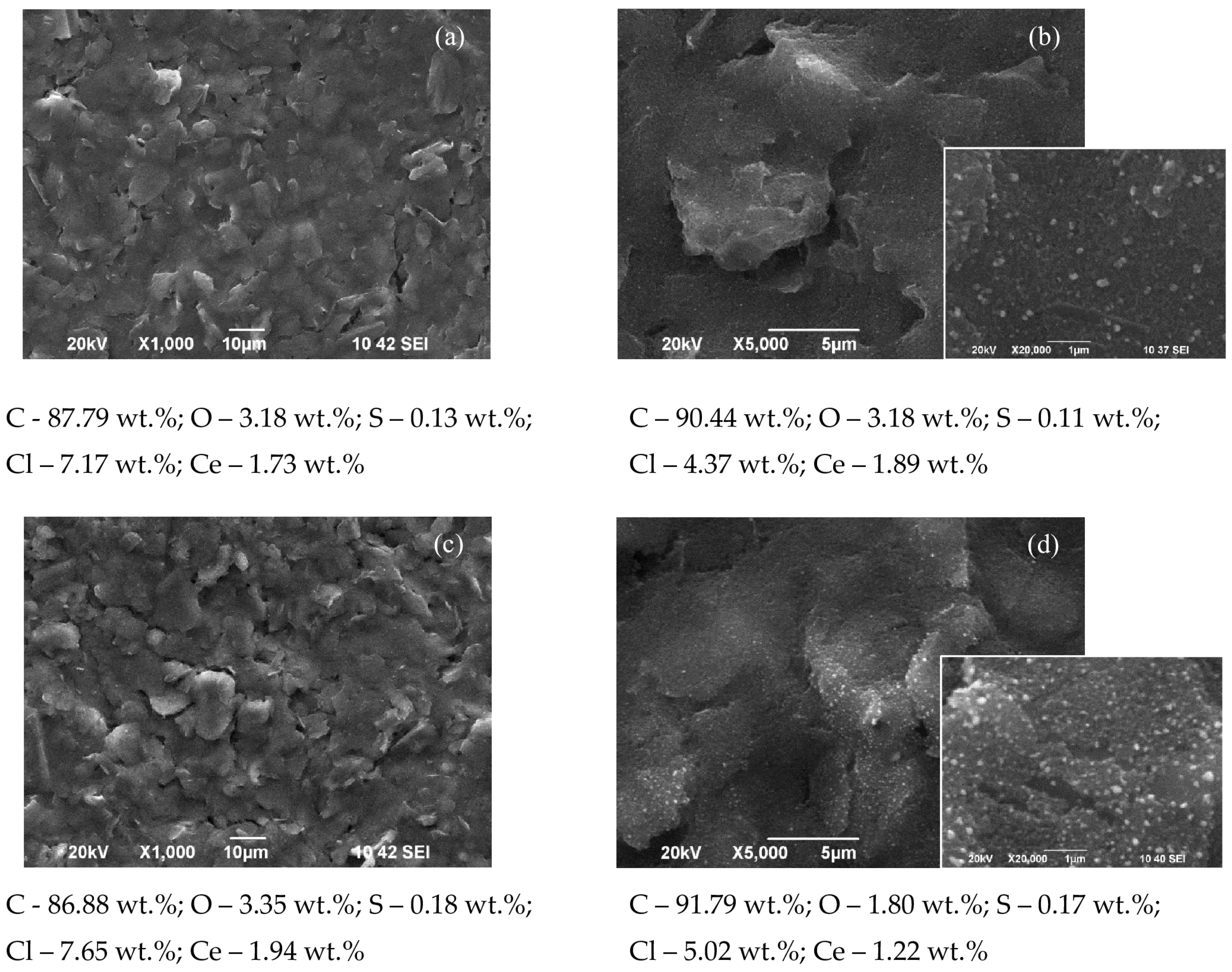
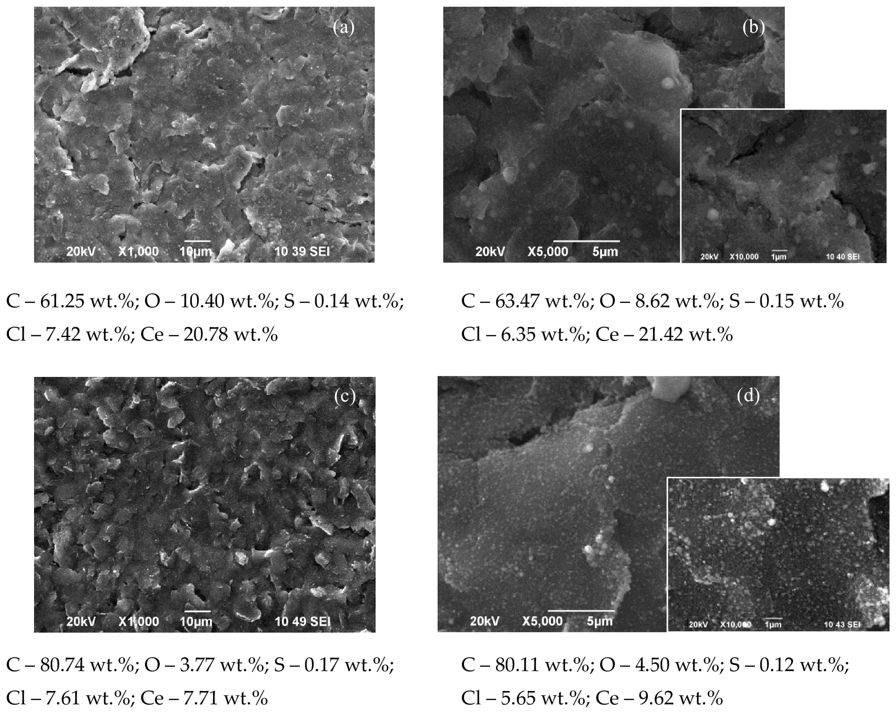
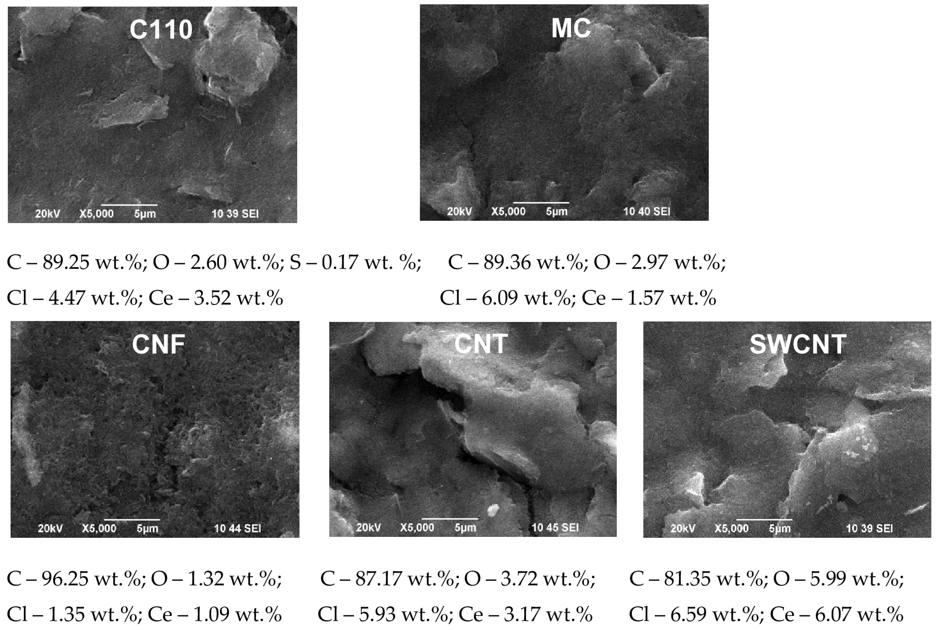
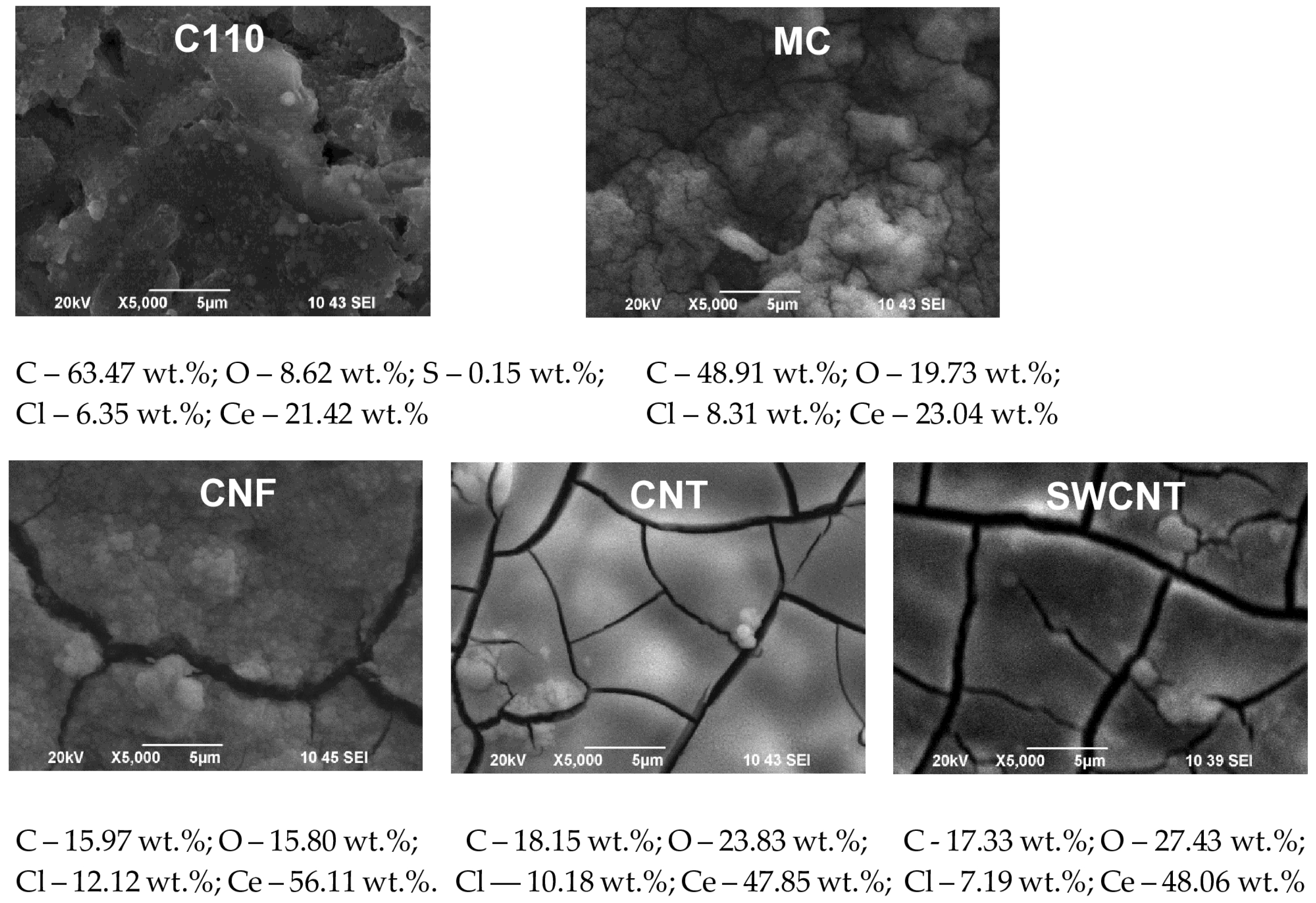
3.1. SEM and EDS Investigations

Part of the results obtained, characterizing the morphology, structure, and chemical composition of coated C110 samples (SEM and EDS), are presented in Figure 1.
According to EDS analysis, the established elements in the bulk of samples are C, S, O, Cl, and Ce. The EDS technique is not suitable for quantitatively determining the C and O contents, but it can qualitatively detect the presence of those elements. Sulfur, which is constantly present at levels below 0.2%, has little effect on the morphology of coatings. It is mainly present in samples with less exposure and, most likely, with thinner coatings, from which we can conclude that it is present in some quantity in the substrate itself. The elements most affected by changes are Cl, Ce, and O. Their amounts depend strongly on deposition time. After 20 min, the amount of Ce is below 2%, comparable to the amount of Cl. After 40 min, it reaches 6–7%, and after 80 min it increases significantly to 60–70%, with a corresponding increase in oxygen. Chlorine is recorded in significantly lower amounts, indicating that cerium oxide may be deposited in two (Ce3+ and Ce4+) conditions.
Coating morphology also depends more strongly on deposition times than on carbon substrate type. At a 20 min deposition time, spherical agglomerations are formed on the surface; after 40 min, leaf-like structures, and after 80 min deposition, dense, cracked coatings, are formed. Detailed information on elemental composition and resulting coating morphology for each substrate is presented below.
The micrograph of C110, electrochemically treated for 20 min in 0.1 M CeCl3x7H2O (Figure 1a, 1000×), illustrates a highly developed, morphologically rough three-dimensional structure. It is dominated by the characteristic leaf-like elements of the C110 surface with sizes in the order of ~5–15 µm. At a magnification of 5000× (Figure 1b) of the same sample, sparsely spaced light sphere-like areas are observed, illustrating formed micro-agglomerates (with sizes ~30–200 nm; see the included inset obtained at magnification 20,000×). Moreover, the number of agglomerates with smaller sizes is dominant. The samples obtained at the higher (0.3 M CeCl3x7H2O) concentration of Ce3+ in the solution are characterized in a similar way (Figure 1c,d). In Figure 1d (see the included inset) it is seen that at the higher concentration of Ce3+ ions in the solution, the number of formed cerium oxide agglomerates increases significantly. Under these preparation conditions, agglomerates with a size of ~120 nm are dominant. At the same time, the comparison of the registered values of the total Ce concentration, at the two concentrations of the solution, does not differ significantly. They vary in the intervals from ~1.7 wt.% for Figure 1a to ~1.9 wt.% for Figure 1c (see the included data of EDS analysis illustrated chemical composition of the studied samples under the pictures).
With increasing electrodeposition time, a gradual increase in the Ce quantity is recorded (up to ~3%, at 40 min of deposition, according to the data recorded in the work protocol). This increase becomes strongly pronounced at a deposition time of 80 min. Figure 2 presents the results obtained with the same compositions and electrodeposition time. They illustrate significant changes in the surface structure and composition of the studied systems. Compared to the deposition time of 20 min (Figure 1), at which the concentration of deposited Ce is relatively low (~1.7–1.9 wt.%), after 80 min of electrodeposition duration it increases significantly (from ~8 to ~21 wt.%—Figure 2). Moreover, it becomes clear that at the higher concentration of Ce3+ in the deposition solution (0.3 M CeCl3x7H2O) the quantity of cerium in the deposited layers is lower (~8%—Figure 2c,d), compared to the layers obtained in 0.1 M CeCl3x7H2O (~21 wt.%—Figure 2a,b). At the same time, with an increase in the concentration of cerium ions in the deposition solution (from 0.1 to 0.3 M CeCl3x7H2O), the sizes of the spheroidal cerium oxide agglomerates forming it decrease significantly, varying in the range of 10–100 nm (Figure 2d). At an electrolyte concentration of 0.1 M CeCl3x7H2O these sizes reach ~1 µm (Figure 2b). Obviously, the significantly larger spherical agglomerates presented in Figure 2b, although fewer in number, include a significantly larger amount of cerium, compared to the micro-agglomerates registered in Figure 2d. While at an electrolyte concentration of 0.3 M CeCl3x7H2O, this amount, is about three times lower. At the same time, however, the specific surface area of many times the number of ceria nano-agglomerates (Figure 2d) exceeds their specific and effective (from a catalytic point of view) surface area by orders of magnitude. These results indicate that by varying the concentration of Ce3+ ions in the solution and the electrodeposition time of the ceria coating, the structure and specific catalytically active surface area of the modified SPCE C110 based on C110 substrate can be influenced in a certain way.
Based on the results presented above, when modifying the surface of SPCEs with a cerium oxide coating, in which the substrate material is CNT, SWCNT, CNF, or MC, the following electrodeposition modes were preferred and applied: current density i = 0.5 mA·cm−2 and 1 mA·cm−2; time of deposition τ = 40 and 80 min; agitation of the electrolytes at 400 rpm of the stirrer. The concentration of cerium ions in the solution was 0.1 M CeCl3x7H2O. The obtained results in a summarized form are presented in Figure 3, Figure 4, Figure 5 and Figure 6. These figures compare the SEM photographic images and EDS data (noted below the figures) of the cerium oxide-modified surfaces of C110, CNT, SWCNT, CNF, and MC electrode substrates with the sequential increase in the change in cathodic current density and deposition time.
Based on the analysis of the results obtained, it was found that when applying:
  • Current density 0.5 mA·cm−2 and electrodeposition time 40 min (Figure 3): The morphology and surface structure of the SPCEs treated in this way practically reproduce those of the untreated substrates. Quantities of cerium oxide deposited were established for: C110 (Ce—3.52%), CNT (Ce—3.17%), and SWCNT (Ce—6.07%). Although a relatively lower quantity of cerium oxide registered on the CNF electrode (Ce—1.09%), it attracts attention with its highly developed surface morphology and structure. With a lower quantity of cerium (1.57%), in this mode, the MC system is also characterized;
  • Current density 0.5 mA·cm−2 and electrodeposition time 80 min (Figure 4): The change in the morphology, structure, and chemical composition of the surface of the such treated SPCE is drastic. The quantity of cerium in the deposited layer is: C110—11.9%; MC—23.04%; CNF—56.11%; CNT—47.85%; SWCNT—48.06%. Accordingly, the modifying surface layer of cerium oxide on C110 is made up of uniformly dispersed spheroidal agglomerates with a diameter of ~0.05–0.2 µm. The surface cerium oxide layer formed on MC is made up of many times larger (diameter ~1–3 µm), densely arranged spheroidal agglomerates, containing cracks with a width of ~0.01–0.05 µm. The morphology and structure of the modified CNF are similar to MC, with fewer but wider cracks, reaching over 1 µm. The electrodeposited cerium oxide layer on the CNT is a dense and smooth coating containing regularly formed cracks with a width of ~0.1–0.5 µm. Similar conclusions are drawn for the modified SWCNT;
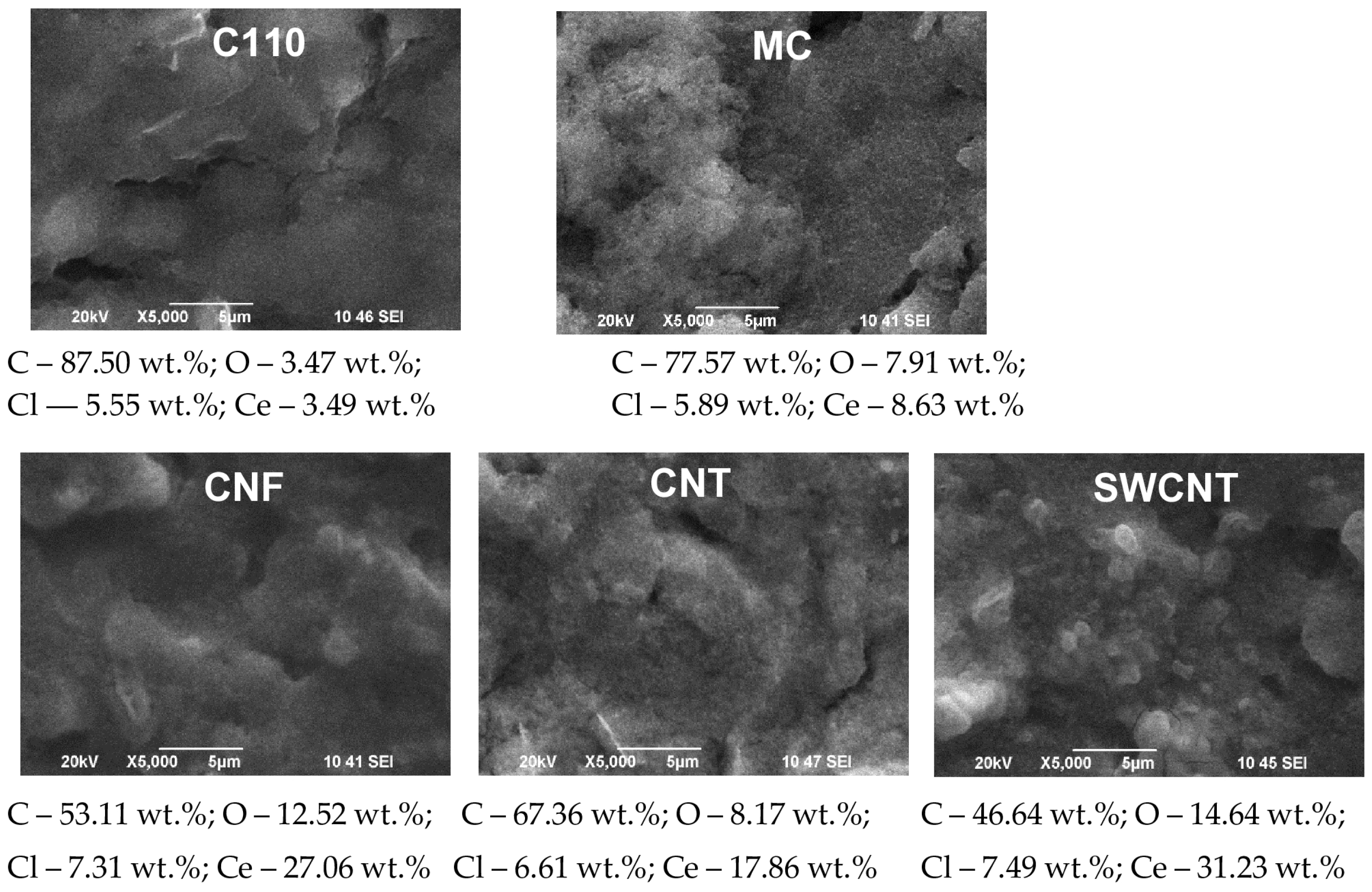
  • Registered differences may be related to the thicker cerium oxide coating deposited at the higher (1 mA·cm−2) current density, evidence for which is the established higher cerium quantity in the studied SPCEs systems: C110 (Ce—3.49%), MC (Ce—8.63%), CNF (Ce—27.06%), CNT (Ce—17.8%); SWCNT (Ce—31.23%);
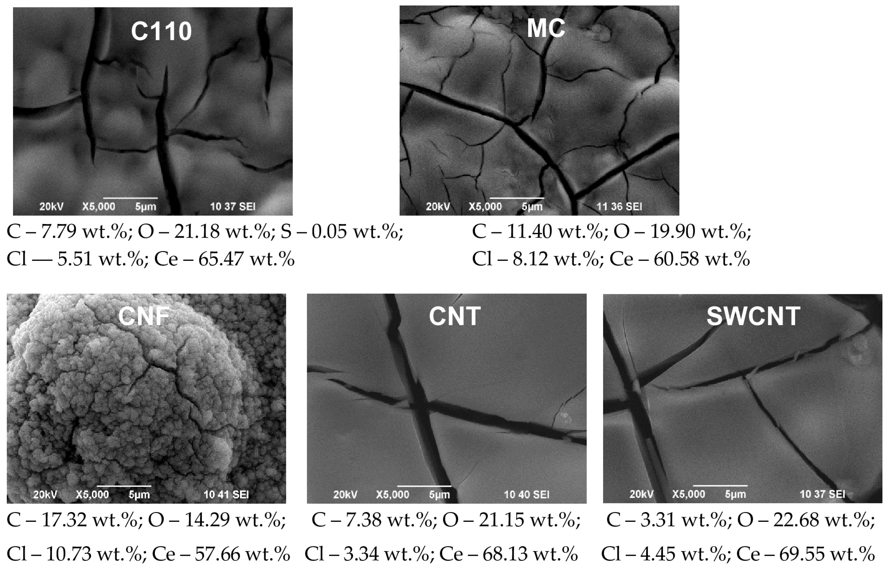
  • Current density 1 mA·cm−2 and electrodeposition time 80 min (Figure 6): The change in the morphology, structure, and chemical composition of the SPCEs treated in this way is even more pronounced. The quantity of registered cerium is respectively: C110 (Ce—65.47%), MC (60.58%), CNF (57.66%), CNT (Ce—68.13%); SWCNT (Ce—69.55%). Accordingly, the modifying surface layer of cerium oxide on C110 is made up of a smooth, dense coating containing regularly formed cracks with a width of ~0.2–1.5 µm. Similar—dense and cracked—are the coatings also deposited on MC, CNT, and SWCNT electrodes. Significantly different in its morphology and structure is the cerium oxide coating deposited on a CNF substrate. It is made up of spheres with a highly developed surface, the diameter of which varies in the range of ~1–7 µm.

3.2. XPS Investigations

The results presented in p.3.1. contain information about the possible prospects for their application in electrocatalytic and electroanalytical aspects. In this regard, however, in addition to the data presented and commented on above, it was necessary to conduct XPS studies. Through them (along with the established morphology, structure, and chemical composition in the volume of the modified SPCEs) the chemical composition of the surface of the samples was characterized, as well as the chemical state of the registered elements, in particular of Ce3+ and Ce4+ (in at.%). In addition, a quantitative assessment was made of the presence and possible changes in the ratio of the concentrations of Ce3+ and Ce4+ in the oxide layers deposited on SPCEs. These data also provide opportunities for effective quantitative assessment when planning the study of ongoing (oxidation/reduction) catalytic processes, respectively electroanalytical studies. The data from the XPS analyses of the studied systems are presented in Table 1 and Table 2.
As expected, with increasing deposition current density, the cerium concentration of the surface cerium oxide layer increases from 5–10 at.% to about 10–15 at.%. Accordingly, this increase is at the expense of the decrease in the carbon concentration. This effect can be associated with an increase in the thickness of the deposited cerium oxide layers, in which the X-ray beam irradiating the layer during analysis cannot reach the carbon substrate. Of course, with increasing deposition time, in the layers deposited at 0.5 mA·cm−2, the concentrations of cerium and, correspondingly, the oxygen associated with it, increase. However, this tendency is not observed for CNT and SWCNT samples. For the SWCNT sample, this decrease is particularly dramatic. In a sample on which the deposition lasted for 40 min, the Ce concentration was close to 15 at.%, while in the one deposited for 80 min, its concentration decreased to 5 at.% (Table 2). It is important to note that the Ce4+ concentration calculated from the Ce3d spectrum is high and reaches about 40–80% of the total amount of deposited Ce.
From the chemical shift of the XPS spectra, the valence state of the elements constituting the deposited oxide layer can be estimated. This information can be taken into account when optimizing the conditions for obtaining mixed Ce2O3 + CeO2 coatings. Figure 7a shows the separated XPS core photoelectron spectra of C1s. The figures present the spectra of samples obtained at 1 mA·cm−2 and a deposition time of 80 min. The spectra of this group of samples are shown because the intensity of the spectra of Ce3d, O1s and C1s is highest and most pronounced in them.
It is important to analyze both the spectra of Ce3d and O1s, as well as C1s, in order to establish the influence of the substrate on the growth of the CeO2 layers.
The peaks in the spectra of C1s are broad. For this reason, they are deconvoluted. The most likely is the peak fitting in which they are divided into three groups. The peaks positioned at 284.6 eV are characteristic of the presence of adventitious carbon [28,29,30] and are most likely not due to the carbon from the substrate. This peak may also overlap with the peak characteristic of the presence of C=C–bond in graphite [31].
The second group of peaks, with a binding energy of about 286.2 eV, is due to the presence of C–O bonds [32,33]. The third group of peaks is positioned at about 288.7 eV and is due to the presence of carboxyl groups [34,35,36]. Figure 7 shows that the intensity, respectively the amount of COOH groups, decreases in the order C110 > MC > CNF > CNT > SWCNT (See Figure 7a). In the C1s spectrum, a group of peaks at low binding energies is also visible, from 282.4 to 283.6 eV. These low energies are characteristic of the presence of metal carbide phases, but in this case they are due to uneven charging of the carbon substrates [37]. We exclude the presence of a metal carbide phase due to the impossibility of obtaining such a phase with the method we used for preparation. Carbon interacts with other elements only at high temperatures, and the cerium layers are deposited when the electrolyte is cooled to 15 °C. At the same time, XRD studies do not show the presence of CeC2. Some authors [38] have shown that graphene can suppress the so-called differential charging effects. They are usually due to samples with insulating domains or island structures that have varying thicknesses on a conducting surface. The spectral features of these areas will be shifted to lower binding energies. These effects, in our opinion, are due to the carbon peaks positioned at 283.6 eV and the lower binding energies at 282.4 eV. At the same time, in MC, CNT, and SWCNT samples, intense peaks appear at about 294.0 eV. They are, in our opinion, again due to this differential charging.
Figure 8 shows the spectra of Ce3d. They consist of spin–orbit split doublets. Each doublet shows an extra structure—satellites—due to final state effects [39]. In the figure, the doublets (v, u and vo, uo) and their satellites (v′, u′, v″, u″, u‴) are denoted by the generally accepted notation of Burroughs et al. [40]. The peaks and satellites characteristic of Ce4+ are marked in red, and the peaks characteristic of Ce3+ are marked in blue. Pardo et al. [41] use the magnitude of u‴—the peak at 916.6 eV, characteristic of Ce4+—to calculate its concentration. It can be seen from the figure (see also Table 2) that the cerium layers deposited on carbon substrates consist of a mixture of Ce3+ and Ce4+. The table gives the ratio between these two oxidized forms of Ce.
Figure 7b shows curve fitted photoelectron spectra of O1s. They consist mainly of three peaks located at around 529.4, 531.5 and 532.5 eV. The peak at 529.4 eV is associated with the presence of the Ce–O bond [42,43,44]. A slight shift of 0.2 eV of the peak of the C110 sample towards lower binding energies—529.2 eV is observed. For the CNF sample this shift is again by 0.2 eV, but towards more positive binding energies—529.7 eV.
The band positioned at 531.5 eV and usually designated OHBE is due to the presence of the double structure in the spectrum of O1s associated with Ce3d. It has been assigned to Ce2O3 oxide on the surface or to hydroxyl groups on the surface or to oxygen chemisorbed on the surface in other forms such as CO, CO2. However, other XPS studies suggested that the presence of the O peak may be attributed to oxide ions in the HBE defective CeOx (x < 2) layer.
The peak at 532.5 eV is typical of the presence of adsorbed OH groups and water [45,46,47].
According to the obtained XPS data, presented in Table 2, the change in the total concentration of cerium (Ce3+ + Ce4+) registered on the surface of the studied systems shows that:
  • At the lower cathode current density (0.5 mA·cm−2), the maximum recorded value for Ce, reaching 11.2 at.%, was recorded on SPCE MC. It is important to note that this sample also recorded the highest value for the Ce4+ concentration—63 at.% (Table 1);
  • Relatively high values of Ce, specifically for the concentration of Ce4+, were also found in SPCEs CNF, CNT, SWCNT, and C110;
  • At the higher cathode current density (1 mA·cm−2), the maximum recorded values of Ce concentration, reaching 14.7 at.% and 11.3 at.%, are registered on SPCEs SWCNT and CNT, respectively. And in these samples, the highest value for the Ce4+ concentration was established—64 at.% (Table 2);
  • Also noteworthy, with regard to the relatively high value of Ce, specifically the concentration of Ce4+, are the results characterizing SPCEs C110 and MC, at a cathode current density of 1 mA·cm−2.
The XPS data obtained and discussed above show that they contain large amounts of Ce3+, which means that the deposited coatings cannot be only CeO2 but should also include Ce2O3. Additionally, the results obtained demonstrate how, by altering the deposition conditions, formed on SPCE coatings with optimal combinations of change the concentration of Ce3+ and Ce4+.

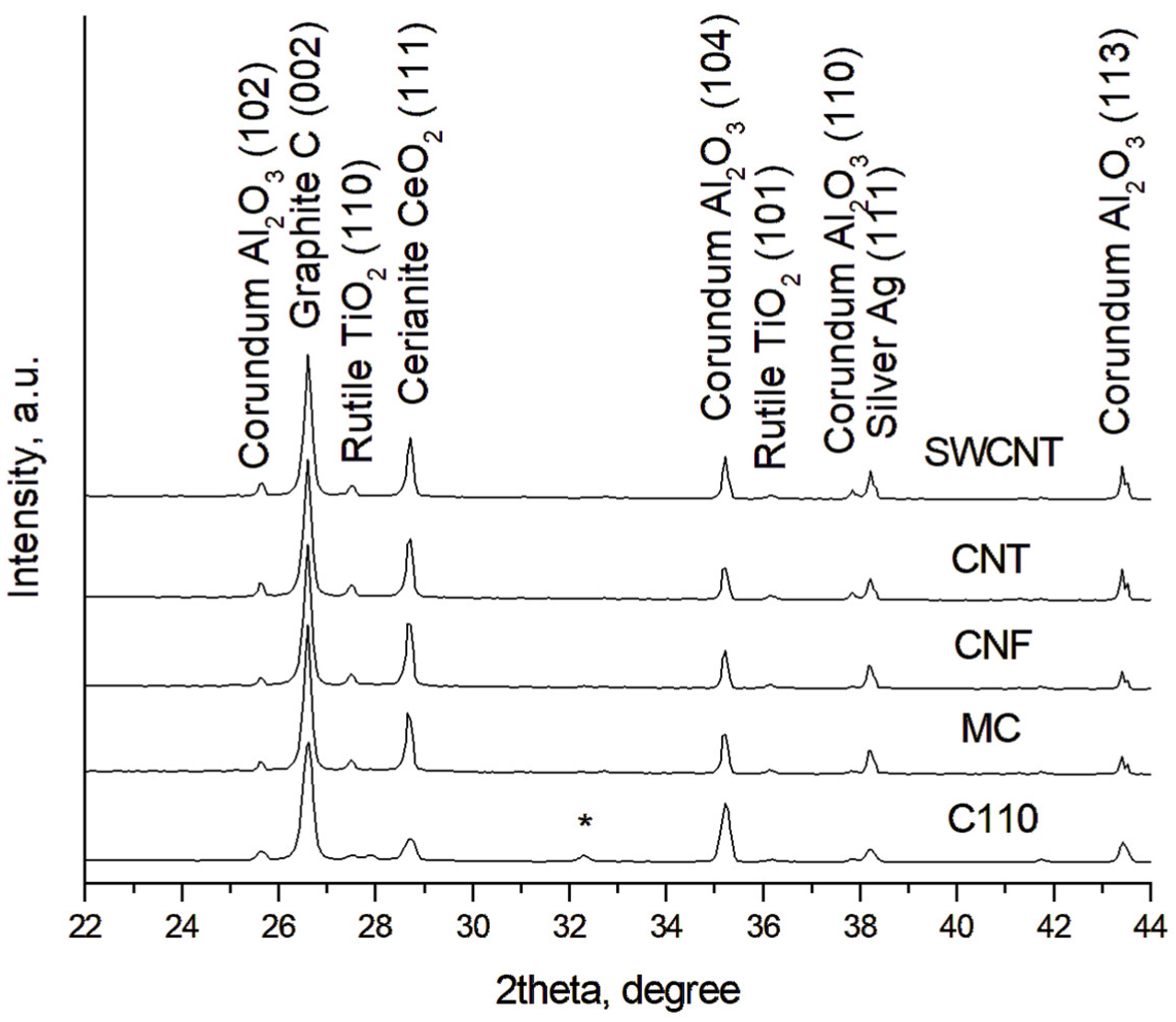
3.3. XRD Investigations

The samples were placed in the diffractometer without any preliminary sample preparation. They were carefully centered relative to the position of the X-ray beam. The processing of the diffractograms and phase analysis were carried out based on Match! [25] and a free crystallographic database, COD [26].
Figure 9 presents the XRD patterns of the studied SPCEs. All screen-printed electrodes were carefully centered so that the X-ray beam fell into the area of the carbon substrates covered with cerium oxide layers—the so-called working electrode of the SPCEs. However, the recorded diffractograms also show the diffraction peaks of the carbon substrate. A small amount of AgCl is detected on C110 and is marked with a star. It is most likely due to the interaction between chlorine ions and silver electrodes. Phase identification showed the presence of corundum (Al2O3 COD Entry # 96-900-9679), rutile (TiO2 COD Entry # 96-900-9084), silver (Ag COD Entry # 96-110-0137) (due to the silver ring forming the reference electrode of SPCE), and graphite (C COD Entry # 96-901-2231). All registered compounds are related to the presence of these elements in the studied electrode substrates. Our studies using EDS from SEM have shown that after the deposition process, cerium appears on the surface. This can be seen from the changes in the diffraction patterns of samples, where a diffraction peak occurs at 28.61 degrees. This position corresponds well with the highest peak of CeO2 (CeO2 COD Entry # 96-900-9009) [48], which suggests that it is this substance that is deposited onto the surface. The appearance of only one diffraction peak of CeO2 is not so unusual and is often caused by a preferred growth direction of the deposited thin film. In our case, this is a plane with Miller indices (111). This has been observed in other methods of growth and formation of CeO2 [49,50].
Since the deposited coatings have an orientation of (111), and the properties of the cerium oxide crystallites are anisotropic, the references to the properties studied during the experiments (such as characterization of corrosion resistance, degradation of dyes, concentration of pharmaceutical forms, etc.) should be related mostly to the crystal plane (111) of the obtained substrates observed in our investigations of cerianite (CeO2).
XPS studies show the presence of large amounts of Ce3+, which is a necessary condition for the formation of Ce2O3. However, according to XRD investigation, this phase has not been detected in the diffraction patterns. More probably, the only conclusion we can draw is that, along with the crystal phase (CeO2), some amorphous Ce2O3 has been deposited.

4. Discussion

In light of the results obtained and commented above (Section 3.1, Section 3.2 and Section 3.3) regarding the formation of Ce–oxide layers, XPS spectra of C1s were also obtained and analyzed. It is observed that in the samples where a carbon peak due to differential charging was registered at the highest binding energies (294 eV), the carbon peaks at the lowest binding energies (283.6 eV) are absent. This is probably related to the differences in the morphology of the carbon substrate, which inevitably affect the growth of mixed Ce2O3 + CeO2 coatings. The question of why in some cases the carbon substrates manage to compensate for this charging, and in other cases not, is debatable. These charging effects are most likely due to the differences in the ability of the layered structures to conduct electrons. Table 2 shows that differential charging does not affect the concentration of Ce4+. In all samples it remains high. At the same time, the concentration of Ce4+ is related to the ionic conductivity of the layers due to the known ability of ceria to act as an oxygen pump—to easily accept and release oxygen ions (the so-called Oxygen Storage Capacity—OSC). For these reasons, we can assume that the sensor properties of the semiconductor materials obtained by us will be due to both the presence of electronic conductivity and the presence of ionic conductivity.
It is also debatable to what extent the C1s peaks, due to differential charging at the highest binding energies (294 eV), should be taken into account in the calculation of the total carbon concentration. If we compare the intensity of Ce3d spectra of SPCEs MC, CNT, and SWCNT samples with those of the other samples, we will see that their area value is comparable to that of the other SPCEs in which they are absent (C1s peaks, due to differential charging at the highest binding energies (294 eV)). For example, in SPCEs MC and CNT, the areas of the Ce3d spectra are 59,846 and 67,186, respectively. The difference between them and the area of the Ce3d peak in the SWCNT sample is greater. In this case, it was calculated to be 39,609. This value is almost half of than in the other two samples. This, and comparing the XPS spectra with the SEM results—the analyses showing dense cerium coatings—gave us the basis to recalculate the atomic percentage concentrations of all elements, without taking into account the C1s peaks due to differential charging at high binding energies (294 eV). These results are given in brackets in Table 2. They show that when we do not take the peak at 294 eV into account in the carbon concentration calculations, the cerium concentration does not decrease, but as expected, increases after 80 min of electrodeposition. On the other hand, this decrease in concentration can also be due to optical effects from a surface that is not uniformly smooth and reflects electrons in different directions due to this unevenness. It is possible that the lower cerium concentration is also due to a thinner deposited layer, which is a result of the presence of diffusion limitations in the transfer of cerium ions in the electrolyte.
For all samples, the areas of the Ce3d peaks compared to the sums of the areas of the two O1s peaks corresponding to the Ce–O bond are approximately equal to the stoichiometric ratio of Ce to oxygen in CeO2. For example, for the SWCNT sample, the area of the Ce3d peak is 37,309/51.6 (51.6 is the Relative Sensitivity Factor (RSF) for Ce3d) = 723, and the sum of the areas of the two oxygen peaks at 529.4 and 531.5 eV is 5184/2.93 (2.93 is the RSF for O1s) = 1769, which is 2.4:1 in favor of oxygen. This ratio suggests the absence of oxygen deficiency, and therefore we exclude the possibility of the presence of oxygen vacancies. This may possibly affect the sensing properties of the obtained electrodes.
The established significant differences and variations in the total and individual concentrations of Ce3+ and Ce4+ in the mixed (Ce2O3 + CeO2) coating, registered on the studied SPCEs, suggest their effective application in the study of both cathodic and anodic catalytic processes. A significant influence in this will obviously be determined by the established morphological and structural changes on the surface of the screen-printed carbon electrodes modified with mixed Ce2O3 + CeO2 coatings. They could have a significant impact on the specific catalytic active surface of the modified SPCEs.

5. Conclusions

An original electrochemical technology (compositions and modes for electrochemical deposition of cerium oxide layers from non-aqueous solutions) has been successfully applied. It allows the formation of promising cerium oxide coatings, with respect to their application as sensors. For this purpose, five types of carbon screen-printed electrodes of the company Metrohm—carbon (C110), mesoporous carbon (MC), single-walled (SWCNT) and multi-walled carbon nanotubes (CNT), and carbon nanofibers (CNF)—were modified with ceria coatings. The qualitative and quantitative changes in the morphology (SEM), structure (XRD), chemical composition (XPS, EDS), and chemical state (XPS) of the elements constituting the electrodeposited cerium oxide coatings as well as the carbon SPCEs were studied. As a result of these studies, the conditions for modifying SPCEs were optimized in order to achieve the desired effect in terms of the structure and chemical composition of the surface of the thus treated SPCEs. In addition, the presence and possible changes in the ratio of Ce3+ and Ce4+ in the cerium oxide layers deposited on SPCEs were established.
As a result of the conducted investigations, it was established that the highest concentration of the modified Ce–oxide layer containing the largest amount of Ce4+ was found on substrates made of mesoporous carbon (MC), single-walled (SWCNT), and multi-walled (CNT) carbon nanotubes. These coatings also have the highest degree of surface charging, as determined by XPS analyses, which can serve as an indication of the presence of both electronic and ionic conductivity. This makes these substrates the most suitable for sensor catalytic systems.
The electrochemical characterization of the capabilities and sensitivity of the thus modified SPCEs is pending with the aim of their application in catalytic and electroanalytical aspects.

Author Contributions

Conceptualization, D.S.; methodology, D.S., R.A., A.T. and G.A.; software, R.A., A.T. and G.A.; validation, D.S., R.A., A.T. and G.A.; formal analysis, D.S.; investigation, R.A., A.T. and D.S.; resources, D.S.; data curation, D.S.; writing—original draft preparation, D.S.; writing—review and editing, D.S.; visualization, R.A., A.T. and G.A.; supervision, R.A., A.T. and D.S.; project administration, D.S.; funding acquisition, D.S. All authors have read and agreed to the published version of the manuscript.

Funding

This research was funded by Project KП-06-M79/1 of the Bulgarian National Science Fund, “Equipment supported/obtained under the project INFRAMAT (National Roadmap for Research Infrastructure)”, financed by the Bulgarian Ministry of Education and Science, and the CoC “Clean technologies for sustainable environment—water, waste, energy for circular economy” (Project BG05M2OP001-1.002-0019), supported by the ERDF within the Bulgarian OP “SESG 2014–2020”.

Data Availability Statement

The original contributions presented in this study are included in the article. Further inquiries can be directed to the corresponding author.

Acknowledgments

The authors are grateful to St. Atanasova-Vladimirova for her assistance with the SEM and EDS assessments. These studies made use of the Electron Microscopy and Microanalysis Laboratory in the Institute of Physical Chemistry—Bulgarian Academy of Sciences.

Conflicts of Interest

The authors declare no conflicts of interest.

Abbreviations

The following abbreviations are used in this manuscript:
SPCEsScreen-printed carbon electrodes
C110Graphite
CNTCarbon nanotubes
SWCNTSingle-walled carbon nanotubes
CNFCarbon nanofibers
MCMesoporous carbon
SEMScanning electron microscope
EDSEnergy dispersive X-ray Spectroscopy
XRDX-ray diffraction
XPSX-ray photoelectron spectroscopy

References

  1. Beitollahi, H.; Mohammadi, S.Z.; Safaei, M.; Tajik, S. Applications of Electrochemical Sensors and Biosensors Based on Modified Screen-Printed Electrodes: A Review. Anal. Methods 2020, 12, 1547–1560. [Google Scholar] [CrossRef]
  2. Antuña-Jiménez, D.; González-García, M.B.; Hernández-Santos, D.; Fanjul-Bolado, P. Screen-Printed Electrodes Modified with Metal Nanoparticles for Small Molecule Sensing. Biosensors 2020, 10, 9. [Google Scholar] [CrossRef] [PubMed]
  3. Rahman, M.M.; Ahammad, A.J.S.; Jin, J.-H.; Ahn, S.J.; Lee, J.-J. A Comprehensive Review of Glucose Biosensors Based on Nanostructured Metal-Oxides. Sensors 2010, 10, 4855–4886. [Google Scholar] [CrossRef]
  4. Mazloum-Ardakani, M.; Beitollahi, H.; Amini, M.K.; Mirkhalaf, F.; Abdollahi-Alibeik, M. New Strategy for Simultaneous and Selective Voltammetric Determination of Norepinephrine, Acetaminophen and Folic Acid Using ZrO2 Nanoparticles-Modified Carbon Paste Electrode. Sens. Actuators B Chem. 2010, 151, 243–249. [Google Scholar] [CrossRef]
  5. Perry Murray, E.; Tsai, T.; Barnett, S.A. A Direct-Methane Fuel Cell with a Ceria-Based Anode. Nature 1999, 400, 649–651. [Google Scholar] [CrossRef]
  6. Uzunoglu, A.; Kose, D.A.; Stanciu, L.A. Synthesis of CeO2-Based Core/Shell Nanoparticles with High Oxygen Storage Capacity. Int. Nano Lett. 2017, 7, 187–193. [Google Scholar] [CrossRef]
  7. Stoukides, M. Solid-Electrolyte Membrane Reactors: Current Experience and Future Outlook. Catal. Rev. Sci. Eng. 2000, 42, 1–70. [Google Scholar] [CrossRef]
  8. Sun, C.; Li, H.; Chen, L. Nanostructured Ceria-Based Materials: Synthesis, Properties, and Applications. Energy Environ. Sci. 2012, 5, 8475–8505. [Google Scholar] [CrossRef]
  9. Asati, A.; Santra, S.; Kaittanis, C.; Nath, S.; Perez, J.M. Oxidase-like Activity of Polymer-Coated Cerium Oxide Nanopartieles. Angew. Chem. Int. Ed. 2009, 48, 2308–2312. [Google Scholar] [CrossRef] [PubMed]
  10. Tsud, N.; Acres, R.G.; Iakhnenko, M.; Mazur, D.; Prince, K.C.; Matolín, V. Bonding of Histidine to Cerium Oxide. J. Phys. Chem. B 2013, 117, 9182–9193. [Google Scholar] [CrossRef]
  11. Qiu, J.-D.; Cui, S.-G.; Liang, R.-P. Hydrogen Peroxide Biosensor Based on the Direct Electrochemistry of Myoglobin Immobilized on Ceria Nanoparticles Coated with Multiwalled Carbon Nanotubesby a Hydrothermal Synthetic Method. Microchim. Acta 2010, 171, 333–339. [Google Scholar] [CrossRef]
  12. Ibrahim, H.; Temerk, Y. Sensitive Electrochemical Sensor for Simultaneous Determination of Uric Acid and Xanthine in Human Biological Fluids Based on the Nano-Boron Doped Ceria Modified Glassy Carbon Paste Electrode. J. Electroanal. Chem. 2016, 780, 176–186. [Google Scholar] [CrossRef]
  13. Ibrahim, H.; Temerk, Y. A Novel Electrochemical Sensor Based on B Doped CeO2 Nanocubes Modified Glassy Carbon Microspheres Paste Electrode for Individual and Simultaneous Determination of Xanthine and Hypoxanthine. Sens. Actuators B Chem. 2016, 232, 125–137. [Google Scholar] [CrossRef]
  14. Temerk, Y.; Ibrahim, H. A New Sensor Based on in Doped CeO2 Nanoparticles Modified Glassy Carbon Paste Electrode for Sensitive Determination of Uric Acid in Biological Fluids. Sens. Actuators B Chem. 2016, 224, 868–877. [Google Scholar] [CrossRef]
  15. Ibrahim, H.; Temerk, Y.; Farhan, N. Electrochemical Sensor for Individual and Simultaneous Determination of Guanine and Adenine in Biological Fluids and in DNA Based on a Nano-In-Ceria Modified Glassy Carbon Paste Electrode. RSC Adv. 2016, 6, 90220–90231. [Google Scholar] [CrossRef]
  16. Ibrahim, M.; Temerk, Y.; Ibrahim, H. Fabrication of a New Biosensor Based on a Sn Doped Ceria Nanoparticle Modified Glassy Carbon Paste Electrode for the Selective Determination of the Anticancer Drug Dacarbazine in Pharmaceuticals. RSC Adv. 2017, 7, 32357–32366. [Google Scholar] [CrossRef]
  17. Andreeva, D.; Ivanov, I.; Ilieva, L.; Sobczak, J.W.; Avdeev, G.; Tabakova, T. Nanosized Gold Catalysts Supported on Ceria and Ceria-Alumina for WGS Reaction: Influence of the Preparation Method. Appl. Catal. A Gen. 2007, 333, 153–160. [Google Scholar] [CrossRef]
  18. Metrohm. Available online: https://www.metrohm.com/bg_bg/search.html?q=electrodes&cat=electrode (accessed on 13 May 2025).
  19. Cherneva, S.; Guergova, D.; Iankov, R.; Stoychev, D. Investigation of Mechanical Properties of Mono- and Multi-Layer Alumina and Ceria Films Using Finite Element Modeling and Nanoindentation Experiments. J. Eng. Mater. Technol. Trans. ASME 2019, 141, 011006. [Google Scholar] [CrossRef]
  20. Nikolova, D.; Stoyanova, E.; Stoychev, D.; Stefanov, P.; Marinova, T. Anodic Behaviour of Stainless Steel Covered with an Electrochemically Deposited Ce2O3-CeO2 Film. Surf. Coat. Technol. 2006, 201, 1559–1567. [Google Scholar] [CrossRef]
  21. Stoyanova, E.; Guergova, D.; Stoychev, D.; Avramova, I.; Stefanov, P. Passivity of OC404 Steel Modified Electrochemically with CeO2-Ce2O3 Layers in Sulfuric Acid Media. Electrochim. Acta 2010, 55, 1725–1732. [Google Scholar] [CrossRef]
  22. Guergova, D.; Stoyanova, E.; Stoychev, D.; Avramova, I.; Atanasova, G.; Stefanov, P. Corrosion Stability of Stainless Steel, Modified Electrochemically with Ce2O3-CeO2 Films, in 3.5% NaCl Media. Bulg. Chem. Commun. 2011, 43, 150–157. [Google Scholar]
  23. Avramova, I.; Suzer, S.; Guergova, D.; Stoychev, D.; Stefanov, P. CeOx/Al2O3 Thin Films on Stainless Steel Substrate - Dynamical X-ray Photoelectron Spectroscopy Investigations. Thin Solid Films 2013, 536, 63–67. [Google Scholar] [CrossRef]
  24. Guergova, D.; Stoyanova, E.; Stoychev, D.; Avramova, I.; Stefanov, P. Self-Healing Effect of Ceria Electrodeposited Thin Films on Stainless Steel in Aggressive 0.5 Mol/L NaCl Aqueous Solution. J. Rare Earths 2015, 33, 1212–1227. [Google Scholar] [CrossRef]
  25. Putz, H.; Brandenburg, K. Match!—Phase Analysis Using Powder Diffraction. Available online: http://www.crystalimpact.com/match/ (accessed on 20 February 2025).
  26. Gražulis, S.; Daškevič, A.; Merkys, A.; Chateigner, D.; Lutterotti, L.; Quirós, M.; Serebryanaya, N.R.; Moeck, P.; Downs, R.T.; Le Bail, A. Crystallography Open Database (COD): An Open-Access Collection of Crystal Structures and Platform for World-Wide Collaboration. Nucleic Acids Res. 2012, 40, 420–427. [Google Scholar] [CrossRef]
  27. Schneider, C.A.; Rasband, W.S.; Eliceiri, K.W. NIH Image to ImageJ: 25 years of image analysis. Nat. Methods 2012, 9, 671–675. [Google Scholar] [CrossRef] [PubMed]
  28. Greczynski, G. Binding Energy Referencing in X-ray Photoelectron Spectroscopy: Expanded Data Set Confirms That Adventitious Carbon Aligns to the Sample Vacuum Level. Appl. Surf. Sci. 2024, 670, 160666. [Google Scholar] [CrossRef]
  29. Jafari, S.; Linford, M.; Sherwood, P. Insight Note. Complications of Magnesium Achromatic X-rays in XPS: A Historical and Practical Perspective. Surf. Interface Anal. 2025, 57, 221–225. [Google Scholar] [CrossRef]
  30. Greczynski, G.; Hultman, L. The Same Chemical State of Carbon Gives Rise to Two Peaks in X-ray Photoelectron Spectroscopy. Sci. Rep. 2021, 11, 11195. [Google Scholar] [CrossRef]
  31. Chen, X.; Wang, X.; Fang, D. A Review on C1s XPS-Spectra for Some Kinds of Carbon Materials. Fuller. Nanotub. Carbon Nanostructures 2020, 28, 1048–1058. [Google Scholar] [CrossRef]
  32. Belmonte, T.; Thiébaut, J.M.; Mézerette, D. Role of Active Species in Surface Cleaning by an Ar-N2 Atmospheric Pressure Post-Discharge. J. Phys. D. Appl. Phys. 2002, 35, 1919–1926. [Google Scholar] [CrossRef]
  33. Greczynski, G.; Hultman, L. Impact of Sample Storage Type on Adventitious Carbon and Native Oxide Growth: X-ray Photoelectron Spectroscopy Study. Vacuum 2022, 205, 111463. [Google Scholar] [CrossRef]
  34. Zhang, B.-B.; Ming, J.; Li, H.-Q.; Song, X.-N.; Wang, C.-K.; Hua, W.; Ma, Y. Structural Characterization of Nitrogen-Doped γ-Graphynes by Computational X-ray Spectroscopy. Carbon N. Y. 2023, 214, 118301. [Google Scholar] [CrossRef]
  35. Lee, J.-W.; Jeong, S.-P.; You, N.-H.; Moon, S.-Y. Tunable Synthesis of Predominant Semi-Ionic and Covalent Fluorine Bonding States on a Graphene Surface. Nanomaterials 2021, 11, 942. [Google Scholar] [CrossRef] [PubMed]
  36. Rojas, J.V.; Toro-Gonzalez, M.; Molina-Higgins, M.C.; Castano, C.E. Facile Radiolytic Synthesis of Ruthenium Nanoparticles on Graphene Oxide and Carbon Nanotubes. Mater. Sci. Eng. B 2016, 205, 28–35. [Google Scholar] [CrossRef]
  37. Biesinger, M.C. Accessing the Robustness of Adventitious Carbon for Charge Referencing (Correction) Purposes in XPS Analysis: Insights from a Multi-User Facility Data Review. Appl. Surf. Sci. 2022, 597, 153681. [Google Scholar] [CrossRef]
  38. Yang, C.-C.; Tsai, M.-H.; Yang, Z.-R.; Yang, Y.-W.; Tseng, Y.-C.; Wang, C.-H. An Effective Charge Neutralization Enabled by Graphene Overlayer in Ambient Pressure XPS Measurements of Insulators. Adv. Mater. Interfaces 2023, 10, 2201926. [Google Scholar] [CrossRef]
  39. Liu, Y.; Huang, J.; Claypool, J.B.; O’Keefe, M.J. Structure and Corrosion Behavior of Sputter Deposited Ce-Al-o Coating on Al 2024-T3 Alloy Substrates. J. Electrochem. Soc. 2016, 163, C198–C204. [Google Scholar] [CrossRef]
  40. Burroughs, P.; Hamnett, A.; Orchard, A.F.; Thornton, G. Satellite Structure in the X-ray Photoelectron Spectra of Some Binary and Mixed Oxides of Lanthanum and Cerium. J. Chem. Soc. Dalt. Trans. 1976, 1686–1698. [Google Scholar] [CrossRef]
  41. Pardo, A.; Feliú, S., Jr.; Merino, M.C.; Arrabal, R.; Matykina, E. The Effect of Cerium and Lanthanum Surface Treatments on Early Stages of Oxidation of A361 Aluminium Alloy at High Temperature. Appl. Surf. Sci. 2007, 254, 586–595. [Google Scholar] [CrossRef]
  42. Jeong, H.-W.; Yun, G.-N.; Bae, Y.-S.; Oh, K.-R.; Hwang, Y.K. Exploring the Role of PdO and Oxygen Vacancies of Pd/CeO2 in Bicarbonate Hydrogenation. J. CO2 Util. 2025, 92, 103028. [Google Scholar] [CrossRef]
  43. Holgado, J.P.; Alvarez, R.; Munuera, G. Study of CeO2 XPS Spectra by Factor Analysis: Reduction of CeO2. Appl. Surf. Sci. 2000, 161, 301–315. [Google Scholar] [CrossRef]
  44. Lopinski, G.P.; Kodra, O.; Kunc, F.; Kennedy, D.C.; Couillard, M.; Johnston, L.J. X-ray Photoelectron Spectroscopy of Metal Oxide Nanoparticles: Chemical Composition, Oxidation State and Functional Group Content. Nanoscale Adv. 2025, 7, 1671–1685. [Google Scholar] [CrossRef]
  45. Lin, Y.-J.; Lee, C.-T. Surface Analysis of (NH4)2Sx-Treated InGaN Using X-ray Photoelectron Spectroscopy. J. Vac. Sci. Technol. B Microelectron. Nanometer Struct. Process. Meas. Phenom. 2001, 19, 1734–1738. [Google Scholar] [CrossRef]
  46. Hoch, L.B.; Wood, T.E.; O’Brien, P.G.; Liao, K.; Reyes, L.M.; Mims, C.A.; Ozin, G.A. The Rational Design of a Single-Component Photocatalyst for Gas-Phase CO2 Reduction Using Both UV and Visible Light. Adv. Sci. 2014, 1, 1–10. [Google Scholar] [CrossRef] [PubMed]
  47. Zhu, Y.; Klingenhof, M.; Gao, C.; Koketsu, T.; Weiser, G.; Pi, Y.; Liu, S.; Sui, L.; Hou, J.; Li, J.; et al. Facilitating Alkaline Hydrogen Evolution Reaction on the Hetero-Interfaced Ru/RuO2 through Pt Single Atoms Doping. Nat. Commun. 2024, 15, 1447. [Google Scholar] [CrossRef]
  48. Wyckoff, R.W.G. Fluorite Structure. In Crystal Structures 1; Interscience Publishers: New York, NY, USA, 1963; pp. 239–444. [Google Scholar]
  49. Breinlich, C.; Essen, J.M.; Barletta, E.; Wandelt, K. Growth, Structure and Electronic Properties of Ultrathin Cerium Oxide Films Grown on Pt(111). Thin Solid Films 2011, 519, 3752–3755. [Google Scholar] [CrossRef]
  50. Nagata, H.; Yoshimoto, M.; Koinuma, H.; Min, E.; Haga, N. Type-B Epitaxial Growth of CeO2 Thin Film on Si(111) Substrate. J. Cryst. Growth 1992, 123, 1–4. [Google Scholar] [CrossRef]
Figure 1. SEM images and EDS data of electrochemically deposited ceria layers on C110 substrate at i = 0.5 mA·cm−2 for 20 min exposure: in 0.1 M CeCl3x7H2O (a) ×1000 and (b) ×5000, and in 0.3 M CeCl3x7H2O (c) ×1000 and (d) ×5000.
Metals 15 00741 g001
Figure 2. SEM images and EDS data of electrochemically deposited ceria layers on C110 substrate at i = 0.5 mA·cm−2 for 80 min exposure: in 0.1 M CeCl3x7H2O (a) ×1000 and (b) ×5000, and in 0.3 M CeCl3x7H2O (c) ×1000 and (d) ×5000.
Metals 15 00741 g002
Figure 3. SEM images and EDS data of electrochemically deposited ceria layers on C110, MC, CNF, CNT, and SWCNT substrates for 40 min, in 0.1 M CeCl3x7H2O at i = 0.5 mA·cm−2.
Metals 15 00741 g003
Figure 4. SEM images and EDS data of electrochemically deposited ceria layers on C110, MC, CNF, CNT, and SWCNT substrates for 80 min, in 0.1 M CeCl3x7H2O at i = 0.5 mA·cm−2.
Metals 15 00741 g004
Figure 5. SEM images and EDS data of electrochemically deposited ceria layers on C110, MC, CNF, CNT, and SWCNT substrates for 40 min, in 0.1 M CeCl3x7H2O at i = 1 mA·cm−2.
Metals 15 00741 g005
Figure 6. SEM images and EDS data of electrochemically deposited ceria layers on C110, MC, CNF, CNT, and SWCNT substrates for 80 min, in 0.1 M CeCl3x7H2O at i = 1 mA·cm−2.
Metals 15 00741 g006
Figure 7. C1s (a) and O1s (b) peaks fitted XPS core photoelectron spectra of samples modified with Ce layers obtained under the following conditions: 0.1 M CeCl3x7H2O, 1 mA·cm−2; 80 min.
Metals 15 00741 g007
Figure 8. XPS Ce3d core photoelectron spectra of Ce layers fabricated under the following conditions: 0.1 M CeCl3x7H2O, 1 mA·cm−2, 80 min.
Metals 15 00741 g008
Figure 9. Comparison of diffractograms characterized phase composition of SPCEs based on C110, CNT, SWCNT, CNF, or MC substrates after their treatment for 80 min in 0.1 M CeCl3x7H2O at i = 1 mA·cm−2 (*—AgCl).
Metals 15 00741 g009
Table 1. XPS data for ceria coatings, deposited on SPCEs at i = 0.5 mA·cm−2.
Type of SPCETime of DepositionC 1s, at. %O, at. %S, at. %Cl, at. %Ce 3d, at. %
(Total Ce3+ + Ce4+)
Ce4+ (% of Ce Total)
C11040 min72.623.11.81.80.736%
80 min65.421.01.08.54.271%
MC40 min69.418.41.27.53.648%
80 min50.427.01.59.911.263%
CNF40 min71.216.40.95.75.762%
80 min52.726.21.611.08.538%
CNT40 min65.719.91.57.85.161%
80 min52.227.41.69.69.349%
SWCNT40 min53.728.50.59.37.974%
80 min52.631.91.25.68.848%
Table 2. XPS data for ceria coatings, deposited on SPCEs at i = 1 mA·cm−2. Results in brackets show concentrations of elements without taking into account peaks of C1s at 294 eV due to differential charging.
Type of SPCETime of DepositionC 1s, at. %O 1s,
at. %
S,
at. %
Cl 2p, at. %Ce 3d, at. %
(Total Ce3+ + Ce4+)
Ce4+ (% of Ce Total)
C11040 min59.222.01.110.07.861%
80 min41.036.12.011.79.379%
MC40 min49.432.81.18.18.765%
80 min48.6
(36.1)
35.7
(41.8)
07.9
(9.3)
7.8
(9.1)
83%
CNF40 min60.824.21.25.97.945%
80 min51.828.01.09.79.652%
CNT40 min47.130.41.110.211.362%
80 min57.9
(39.5)
29.6
(42.5)
1.0
(1.4)
3.2
(4.6)
8.3
(11.9)
64%
SWCNT40 min37.537.11.39.414.764%
80 min65.1
(35.4)
26.8
(49.7)
1.2
(2.2)
2.3
(4.3)
4.5
(8.4)
44%
Disclaimer/Publisher’s Note: The statements, opinions and data contained in all publications are solely those of the individual author(s) and contributor(s) and not of MDPI and/or the editor(s). MDPI and/or the editor(s) disclaim responsibility for any injury to people or property resulting from any ideas, methods, instructions or products referred to in the content.

