Article

Upset Resistance Welding of a Microcomposite Cu-Nb Conductor for Pulsed Power Applications

by
Nikolaj Višniakov
1,*,
Paulius Beinoras
2 and
Oleksandr Kapustynskyi
2
1
Institute of Mechanical Science, Vilnius Gediminas Technical University, Plytines g. 25, LT-10105 Vilnius, Lithuania
2
Department of Mechanics and Material Engineering, Vilnius Gediminas Technical University, Plytines g. 25, LT-10105 Vilnius, Lithuania
*
Author to whom correspondence should be addressed.
Metals 2025, 15(4), 394; https://doi.org/10.3390/met15040394
Submission received: 3 March 2025 / Revised: 28 March 2025 / Accepted: 29 March 2025 / Published: 1 April 2025
(This article belongs to the Section Welding and Joining)

Abstract

The present study offers an experimental investigation into the welding of Cu–Nb wire using upset resistance welding. The aim is to examine the structure, as well as the electrical and mechanical properties, of Cu–Nb conductor joints produced by this method, which are intended for use in coils in pulsed magnetic systems. Analysis of the joint structure revealed that it was free from welding defects. The welded joint demonstrated a negligible change in electrical resistance while retaining sufficient ultimate strength and plasticity comparable to the base material. The tensile strength of the welded sample was found to be 620 MPa. The heat-affected zone is narrow, and the heating temperature is lower than the melting point of the composite material. Therefore, welding occurs in the solid phase without remelting the Cu–Nb composite wire or destroying its unique microstructure. Thus, upset welding is a promising technology for use in solenoid terminal connections with external electrical circuits that are not directly exposed to the high magnetic or tensile forces generated inside a solenoid of a pulsed magnet system.

1. Introduction

One of the most significant unresolved challenges in strong magnetic field technologies is the development of reliable welded joints for high-strength microcomposite conductors. This challenge could theoretically be addressed using specially developed welding methods.
This article investigates the impact of butt resistance welding parameters on the electrical and mechanical properties of Cu–Nb conductors. Cu–Nb microcomposites are considered among the most promising and suitable materials for pulsed systems operating under strong magnetic fields. The structure of Cu–Nb microcomposite conductors consists of a copper matrix embedded with very thin niobium filaments. These Nb filaments reinforce the copper matrix, enhancing the mechanical strength of the conductor without hindering electron flow, i.e., the flow of electric current. The method used for manufacturing these composite conductors, known as “assembly-deformation”, is similar to the production of bimetals. It involves winding Cu tubes and Nb rods followed by intensive repeated deformation. Small-scale production of such wires has recently begun, with an annual production volume reaching up to 50 tons per year [1,2].
Previous studies [3,4,5,6] analysed the structure and mechanical properties of Cu-Nb conductor joints welded using methods that involve melting of the base material in the weld zone. These studies also presented methodologies for various welding techniques and the selection of optimal welding parameters and conditions, while comparing experimental data with calculated results [7]. A detailed analysis of the welded joint’s structure and the results of material testing provided valuable insight into the most effective welding procedures for composite Cu-Nb conductors.
However, certain aspects remain unexplored or unanalysed. Until now, research has focused primarily on metal matrix welding or full composite deposition methods. Significant findings have emerged from studies on thermite welding (TW), laser welding (LW), electron beam welding (EBW), and resistance welding (ERW) of Cu-Nb composites during the alignment of the composite or its matrix [3,5,6,8,9].
Since 2018, a series of ISO 17279 standards [10] have been implemented to define microwelding technology and testing requirements for Cu/Nb-Ti and Nb-Ti superconductors. These standards primarily address thin, multilayer microfusion superconductors and solid-state diffusion microconnections, down to a thickness of 100 µm. Autogenous overlap-free coupling of the lap and bridge joints has been achieved by pressing and heating the joint in a vacuum chamber. However, the feasibility of welding Cu-Nb and similar microconductors in the solid-state using pressure welding methods, such as diffusion or butt resistance welding, has not yet been thoroughly investigated [7,11,12]. Since no melting occurs, the weld metal retains many characteristics of the multiphase base material. Welds exhibit a hot-worked structure, making them metallurgically closer to the base material, with minimal disruption to compositional gradients and the second phase, which does not significantly affect weldability. Solid-state welding can eliminate or minimise most problems encountered with fusion welding because the temperatures are lower, avoiding transformations, solidification stresses, or cracking caused by melting, environmental reactions, phase interactions, or structural softening. The resulting microstructure is notably different, featuring flow patterns rather than the solidification structures typically found in fusion welds.
Therefore, refractory, reactive, heat-sensitive, and multiphase metals and materials can be effectively joined using solid-state welding techniques [13,14]. In his section on welding metal matrix composites, Massler suggests that non-fusion processes are preferable for joining advanced metals and alloys. He also highlights that, in resistance welding, benefits are achieved by minimising the time spent at peak temperature
Contact butt welding is a thermomechanical pressure welding method that can be performed with or without metal melting. When the joint is heated only to a plastic state, without reaching fusion, it is referred to as resistance welding, a form of solid-state welding. Resistance-affected welding is especially compatible with other solid-state welding methods because it offers greater control over both process parameters and weld reliability compared to other techniques [15,16]. Equipment for upset welding is relatively simple, easy to operate, and easy to maintain. The fixtures are uncomplicated, the setup is minimal, and only a few welding variables need to be monitored and controlled.
This welding method presents challenges in ensuring uniform heating across the joint surface. Consequently, resistance welding is used primarily to join small-section products with simple profiles, typically having a diameter or side length of up to 20 mm, such as circles, squares, hexagons, wires, and small-diameter thick-walled pipes. Unlike welding parts with complex or large cross-sections, resistance welding of small-diameter wires does not result in significant uneven heating. Therefore, a large welding force and extensive deformation are not necessary. However, this method is versatile and can also join various non-ferrous metals, heavy alloys, and parts with small and large diameters or complex sections [17,18,19].
An important feature of contact resistance welding and diffusion bonding is their minimal thermal effect on microcomposite fibers [20,21,22]. In diffusion bonding, the heating temperature is significantly lower than the melting temperature, but the process generally requires a longer duration to achieve a proper bond. In contrast, contact-resistance welding operates at higher temperatures but with extremely short heating durations, lasting only a fraction of a second. Therefore, resistance welding is a highly efficient method for joining materials compared to many traditional welding techniques, including arc welding. Furthermore, the deformation in resistance welding helps to expose fresh metal at the weld interface, effectively eliminating contaminants and residual surface oxides [16,23]. Residual deformations in resistance welding are reduced and more localised compared to those in flash welding and arc welding methods. This is because the joint forms across the entire section, concentrating deformations only at the joint, resulting in uniform reinforcement throughout the section [24].
The primary objective of this research is to experimentally weld and test Cu-Nb conductor resistance-welded joints to evaluate the effectiveness of this method for joining Cu-Nb composites. Furthermore, this study investigates how the technological parameters of resistance welding influence the microstructure, as well as the mechanical and electrical properties, of Cu-Nb composite joints.

2. The Peculiarities of Resistance Welding for Copper and Copper-Based Materials

Most metals can be joined using resistance butt welding, a method that is popular and widely practiced due to its versatility. However, resistance welding of copper and copper-based alloys presents challenges due to the high electrical and thermal conductivity of the material, as well as the very narrow temperature range within which it can be pressure welded [25,26].
In addition, the weldability of copper and its base alloys, assessed by the ratio of thermal conductivity to electrical conductivity according to the Wiedemann–Franz law, is below 0.25 [27,28]. Therefore, in practice, copper, its alloys, and metal composite materials with electrical conductivity greater than about 30% IACS can be resistantly welded [29]. Taking into account the physical properties and patterns described above for the Cu-Nb conductor (Table 1 and Table 2), we can assess the weldability of Cu-18 wt% Nb. The niobium content in the microcomposite wire is approximately 0.2. Furthermore, the melting point of copper in this composite material, Tm (Cu), is significantly lower than half the melting point of niobium Tm (Cu < 0.5 TmNb).
According to ISO/TR 25901-3 [33], resistance welding is classified as a type of pressure welding and includes two primary types: flash and upset resistance welding. This process is conceptually similar to the method used in the production of Cu-Nb conductors. In butt contact welding, the edges of the parts are heated to a plastic state, whereas fusion welding involves heating the welded edges until a layer of molten metal forms.
The fusion welding capabilities of Cu-Nb conductors have been previously analysed, with joint characteristics detailed in our earlier publications [3,5,6,9]. However, copper conductors and wires with a small diameter (up to 5 mm, corresponding to a cross-section of up to 20 mm2) are typically welded using the resistance-welding method [34,35]. This technique is classified as solid-phase welding, based on the state of the metal in the welding zone.
There are three types of resistance welding: increased deposition pressure welding, constant-pressure welding, and pulsed welding with increased deposition pressure [36]. Constant-pressure welding is not suitable for copper wires and cables [34,35,37].
In resistance welding, end surfaces are heated to 70–90% of their melting temperatures. Typically, the surfaces to be joined are covered with oxide films. During the upsetting phase of flash contact welding, these films are destroyed by plastic deformations and are completely removed in a flash. However, in upset resistance welding, complete removal of oxide films from the joint zone may not occur due to the relatively small shear plastic deformations needed to form metallic bonds in the solid-state welding process. With this method, the degree of plastic deformation is generally insufficient to completely destroy and remove all oxides. Consequently, only about 60–70% of oxide ends are typically removed from the surface, which can result in relatively low ductility in the joints [35]. However, despite this, the application rate of flash welding in practice is no more than 10% of the total number of resistance welding joints.
When using resistance upset welding, careful preparation and precise alignment of the edges are crucial to ensuring uniform compression across the entire cross-section, particularly for small-diameter wires. The gap between the ends during resistance welding must not exceed 0.5 mm. To achieve clean contact surfaces, mechanical cleaning and grinding are recommended, followed by etching with caustic soda (sodium hydroxide, NaOH) or carbon tetrachloride (CCl4), and then rinsing with water. Additional etchants, such as a 10% sulfuric acid solution or sodium bichromate (Na2Cr2O7), can also be used to remove oxide films [38].
The main technological parameters of resistance upset welding (as shown in Figure 1) include the welding current (Iw) or current density (j), the voltage of the machine’s secondary circuit (U2), the heating time of the parts (tw), the upset allowance (Δu), the base length (l0), the welding pressure (Pw), and the upsetting pressure (Pu), which correspond to the welding force (Fw) and the upsetting force (Fu), respectively [39,40].
Small-diameter wires made of copper and dissimilar metals are welded using resistance welding under demanding conditions, with welding times up to 1.5 s. More stringent welding modes, involving shorter welding (heating) durations, are employed as the thermal conductivity of the metal increases. A hard welding mode localises heat release to a very narrow contact zone, significantly reducing the impact of the thermophysical properties of the weld metal on heating and diffusion processes [41].
According to various sources, pure copper cores with diameters ranging from 0.4 to 2 mm are welded at a current density of 250–300 A/mm2, with an average heating temperature of approximately 0.8–0.9 Tm. For copper alloys, a small welding pressure of 3–9 MPa is applied because their yield strength (Re) at high temperatures above 900 °C is about 10 MPa. Weld pressure, which compresses parts during the flow of the welding current, significantly influences heat release during the heating stage [42,43,44]. The lower welding pressure (Pw) value increases contact resistance between parts, leading to increased heating and increased oxidation at the joint.
When the welding force is reduced, all other factors remaining constant, the intensity of the heat generation increases. However, this reduction also results in greater unevenness in heating across the cross-section of the contact parts due to random distribution of the contact areas. This uneven distribution is a significant disadvantage of resistance welding.
To achieve high-quality joints during resistance butt welding, the focus is to ensure uniform heating of the part ends and consistent metal deformation. Uniform heating maximises the destruction and removal of oxides. During the upsetting process, metal heated to high plasticity is squeezed toward the peripheries, carrying oxides along with it, which are expelled as part of the process [45,46].
High upsetting pressure (150–400 MPa) is necessary for welding metals with high thermal conductivity, such as copper and aluminum alloys [42,43,44]. In upset resistance welding, it is crucial to precisely select both the compression force and the optimal (minimum) base length. This ensures sufficient rigidity of the welded components and minimises heat transfer to the contact electrodes. For copper alloys, resistance welding requires a base distance larger than that used for steels, along with specially designed clamps to minimise the deformation area in welded joint.
Special non-conductive collets are commonly used to prevent deformation of copper parts caused by increased base length [47]. These collets help localise plastic deformation within the resistance-welded joint zone, ensuring the complete extrusion of oxides and removal of grates. An ideal butt weld is spatter-free, smooth, and symmetrical, although it often exhibits a slight thickening in the weld area due to metal deposition, which is typically not removed mechanically after upset welding. In most cases, the level of heating during contact welding is controlled by monitoring the deposition of the workpieces and, less frequently, by measuring the duration of their heating. In the first method, the welding current is automatically turned off once the workpieces reach specified size.
Weld quality can be significantly improved by protecting the weld zone with shielding gases such as argon, helium, or gas mixtures, or by using vacuum welding, which involves a hood with exhaust air. These methods are often employed when welding expensive or highly oxidisable metals, where minimising metal loss and preventing oxidation are critical [15,48,49].
Surface coatings are also used to simplify the welding of challenging material combinations, enhance the heat balance at the weld interface, or address solubility issues, particularly in flash welding. During pressure welding, most coatings are squeezed out, but some remain at the weld interface. This helps to reduce the formation of thin, brittle intermetallic particles or layers [50,51].

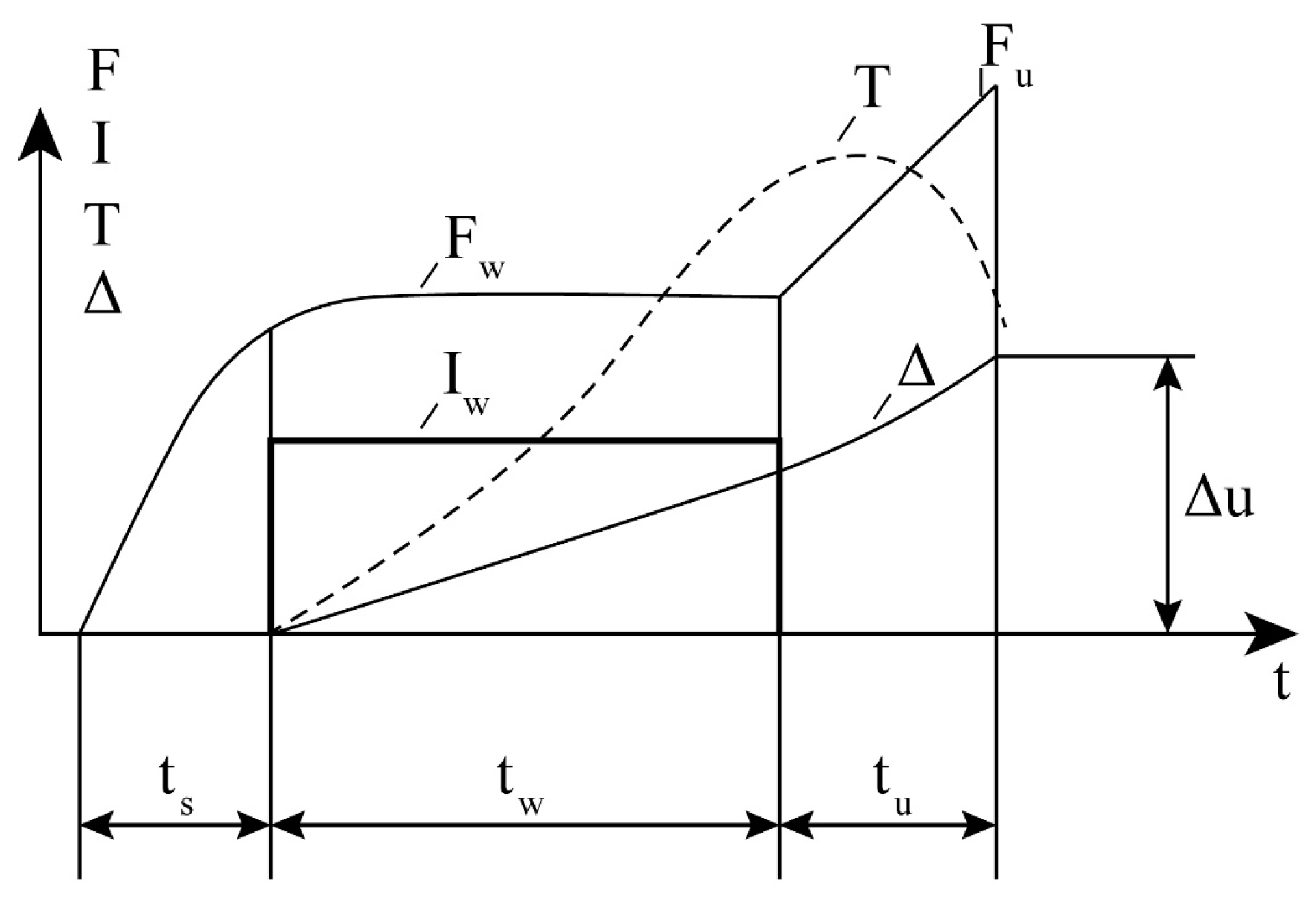
3. Calculation and Selection of Welding Parameters

Despite the fact that the applied resistance-welding method is well known and has been used for a long time, it is very difficult to find a standardised method for the selecting or calculating of optimal welding parameters. Much useful information about welding quality and joints testing can be found in any EN and ISO standards. General information on standards related to resistance welding is provided in standard ISO/TR 23413:2019 (Resistance welding—Overview of standards for resistance welding) [52]. Since there is no detailed information about the calculation methodology of welding regimes described in any standards or guidelines, the applied methodology of calculation of welding parameters and all equations that were found in various academic and scientific literature are presented in Section 3.
During resistance welding, the welded parts are heated by an electric current Iw passing through them, releasing heat Q due to the total electrical resistance R of the parts, as described by the Joule–Lenz law [43,53]:
Q = 0.24   R I w 2   t w
where Q—the heat generated (cal); Iw—the current passing through the metal joint (A); R—the total resistance of the parts (Ω); tw—duration of the current flow (s).
In resistance butt welding, selecting mode parameters often begins by determining the correct ratio of current density (A/mm2) to heating duration (s) using an empirical equation. The approximate values of the current density (j) are calculated using the following equation [35,41]:
j = t w = k · 10 3
where j—current density, A/cm2; tw—welding time, s; k—coefficient for copper 27.
Materials with high thermal conductivity require a longer stick-out to minimise heat loss to the machine’s jaws and to establish an optimal heating zone for the parts. The minimum base length for welding copper wires or small-diameter rods can be calculated using the following equation [47]:
l 0 = ( 2 3 ) · d
where d—diameter of the welded part, mm.
The final operation in butt welding is disturbing, a process that involves the necessary plastic deformation of the metal, known as the upset allowance (Δu). In resistance welding, upsetting begins under the influence of the welding pressure (Pw) once the welding current is activated and the metal starts to heat up. It concludes after the current is turned off, under the influence of the upsetting pressure (Pu). If the upset allowance (Δu) is too small, oxides can remain in the joint, leading to insufficient penetration. Conversely, an excessive upset allowance (Δu) can result in bending the fibers in the joint area. Therefore, the upset allowance (Δu) must be carefully optimised.
The upset allowance (Δu) can be determined using the following equation [47]:
Δ u = ( 0.2 0.3 ) · d
where d—diameter of the welded part, mm.
In butt upset welding of copper alloys, welding pressure (Pw) typically ranges from 3 to 9 MPa. Research data [45,46] indicate that the Cu–Nb composite retains 50% of its strength and hardness at temperatures above 500 °C. With this in mind, the yield strength of Cu-Nb wire at temperatures between 878 °C and 1085 °C should decrease by approximately half, not exceeding 416 MPa. Other studies [47,48] show that the yield strength of the Cu–Nb microcomposite decreases significantly at temperatures between 700 °C and 1000 °C, failing to reach 468 MPa, with elongation reduced to 6.4%. The decline in yield and ultimate strength above 500–700 °C is associated with niobium coagulation processes [5,49]. It is important to note that these mechanical property values were obtained during 1 h annealing of Cu–Nb wire at extremely high temperatures. During this process, niobium fibers undergo coagulation, significantly softening the composite at temperatures of 700 °C and higher. The softening of the Cu–Nb composite after annealing is also accompanied by the relaxation of macrostresses in the niobium fibers and the recovery of their properties to standard levels. Calculations for Cu–Nb microcomposite wires with niobium fibers indicate that heat treatment at temperatures above 500 °C for 1–3 h will only initiate coagulation processes, driven by the diffusion of niobium into the copper matrix. Therefore, in this scenario, the applied welding pressure should not exceed Pw = 416 MPa, and the welding force should be approximately 4160 N.
Deformation of contact points begins when the upsetting pressure (Pu) exceeds the yield stress (σγ) and stops when the upsetting pressure equals the yield stress (Pu = σγ). The upsetting pressure (Pu) can be roughly calculated using the following equation [35]:
P u = ( 1 + 0.125 · α   · S W · L ) · σ γ
where α—stress factor (for a circular section it is 1.3; for a square—2; for a rectangle—2.3; for sections of complex shape—2.5); S—cross-sectional area, mm2; W—heating width of one part above temperature 900 °C, mm; L—cross-sectional perimeter of the material, mm; σe—strength of the material at an average temperature from 900 °C to welding temperature, MPa.
Workpiece heating width can be approximately calculated using the following equation [35,43]:
W = α · t w
where α—thermal diffusivity of welded metal, cm2/s; tw—welding time, s.
Upsetting force (Fu) can be approximately calculated as the product of deposition pressure and cross-sectional area using the following equation [34,54]:
F u = P u · S
where Fu—upsetting force, N; Pu—upsetting pressure, MPa; S—cross-sectional area of samples, mm2.
The clamping force (Fc) applied to the parts in the clamps is calculated to ensure the parts remain securely in place and do not slip during the laying stage. It is determined using the following equation [35]:
F c = k 0 · F u
where ko—sliding friction coefficient, dependent on clamp pair characteristics, metal being welded, clamp design, and part shape (for a copper–copper metal pair, k0 = 1 ) ; Fu—upsetting force, N.
The minimum welding current required to heat contact to a given temperature can be calculated using equation [35]:
I w = T w 0.24 ( k · ρ t · t w c · γ · S 2 + m · R 1 · t w S · π · c · γ · λ )
where Tw—the transition temperature at the end of heating is taken as equal to 0.8–0.9 or equal to the melting point of the base metal, °C; k—loss coefficient (equal to 0.75 for non-ferrous metals); ρ or ρt—electrical resistivity of a metal up to melting temperature, Ω·cm; tw—welding time, s; γ—density of weld metal, g/cm3; c—specific heat of the metal, cal/g·°C; m—change coefficient of contact resistance during welding (equal to 0.4 for non-ferrous metals); R1—total resistance at the beginning of welding, Ω; S—cross-section of the welded part, cm2; λ—thermal conductivity coefficient, cal/cm·s·°C;
The electrical resistance of the parts being welded, along with their contact points, significantly affects heat release during resistance butt welding. This, in turn, influences the size and strength of the welded joint. The total resistance of the parts during resistance welding is generally determined by the following equation [43,45]:
R = 2 · R d + R c + 2 · R e
where Rd—resistance of parts (depending on minimum base length), Ω; Rc—contact resistance between parts, Ω; Re—electrode-part resistance, Ω;
In resistance welding, the majority of heat (85–90%) is generated due to the inherent resistance of the parts (Rd). Although in butt resistance welding, the proportion of heat generated specifically at contact resistance between parts is relatively small—typically not exceeding 10–15%—this contact resistance (Rc) still plays a crucial role in heating the welding zone. Heat is generated in a narrow contact zone over a brief period, leading to a rapid increase in temperature. This elevated temperature persists even after contact resistance diminishes until the completion of the welding cycle, resulting in this area being heated more intensely than others. During butt resistance welding, contact resistance (Rc) decreases swiftly. Initially, Rc is relatively high due to the low pressure applied at the ends, but as the temperature rapidly rises to 600–700 °C, contact resistance nearly vanishes. Further heating occurs through the specific electrical resistance of the parts themselves. Consequently, contact resistance (Rc) can often be considered negligible due to the thorough preparation of mating surfaces, high electrical conductivity of materials, and substantial compressive pressure applied. Typically, Rc does not exceed 3 µΩ. The electrode-to-workpiece resistance (Re) remains low during the welding process and has minimal impact on the heating of the joint. This is primarily due to the relatively large distance from the welding zone and the extensive contact area involved. According to Holm’s work, the resistance of cold parts (2Rd) is determined by the resistivity (ρ0), the length (l0), and the cross-sectional area (S) [35,41].
2 · R d 1 = k n · ρ 0 · l 0 S
where kn—coefficient that takes into account the uneven distribution of current strength across the cross-section of the conductor (for copper—0.9); ρ0—resistivity of the workpiece material at current temperature, µΩ·cm; l0—base length, conditionally equal to the distance between the jaws, cm; S—cross-sectional area of the workpiece, cm2.
The dependence of the electrical resistivity of a metal on temperature can be described by the following formula [41]:
ρ t = ρ 0 ( 1 + α · T )
where ρt—(specific resistance) electrical resistivity of the metal at temperature T, Ω cm; ρ0—electrical resistivity of the metal at room temperature, Ω·cm; α—temperature coefficient of electrical resistance (equal to copper ~0.004).
The resistance of hot parts, 2Rd2, is determined by the specific resistance ρt at the average heating temperature of the parts (for resistance welding, Tav = 0.33 Tw), the base length l0, and the cross-sectional area S [35,41]:
2 · R d 2 = ρ 0 ( 1 + α · T a v ) · l 0 S
where ρ0—electrical resistivity of the metal at room temperature, Ω cm; α—temperature coefficient of electrical resistance (equal to copper ~0.004); base length l0, cm; cross-sectional area of the workpiece S, cm2.
Contact resistance Rc between connecting surfaces can be approximately calculated using the formula proposed by Holm or the following empirical equation [23,43,55,56,57]:
R c = r c F φ
where rc—contact resistance at a load of 1 kg., which corresponds to copper alloys (1–2) 10−3 Ω; φ—the exponent, depending on the material and surface preparation, is in the range of 0.5–1.0 (0.7 for contact of a Cu–Cu pair); F—contact compression (in this case equal to Fw), kg
However, this formula does not take into account the surface condition of the parts and assumes that the contact resistance (Rc) is independent of the size of the parts. Therefore, it is suitable only for approximate calculations. In resistance-based metal heating, the process can occur at any secondary voltage. This is in contrast to flash welding, where the joining process remains stable only within specific minimum voltage limits. Beyond these limits, melting can continuously transition into an arc.
The achievable temperature of the junction heating, derived by transforming Equation (9), can be calculated using the following equation [43]:
T = 0.24 · I 2 k · ρ t · t w c · γ · S 2 + m · R 1 · t w S · π · c · γ · λ
where T—the transition temperature at the end of the heating is taken, °C; k—loss coefficient (equal to 0.75 for non-ferrous metals); ρt—electrical resistivity of a metal up to melting temperature, Ω·cm; tw—welding time, s; γ—density of weld metal, g/cm3; c—specific heat of the metal, cal/g·°C; m—change coefficient of contact resistance during welding (equal to 0.4 for non-ferrous metals); R1—total resistance at the beginning of welding, Ω; S—cross section of the welded part, cm2; λ—thermal conductivity coefficient, cal/cm·s·°C; I—welding current, A.

4. Results of Calculating Upset Welding Parameters

Upset welding parameters were calculated under the condition that the welding duration should not exceed 1.5 s and the joint temperature should not surpass 1085 °C. The results of the welding mode calculations are presented in Table 3, Table 4 and Table 5 and Figure 2. For small-diameter conductors, the resistance of the welding circuit depends mainly on the metal’s resistivity (Rd). Due to careful surface preparation—such as polishing and etching the contact resistance (Rc) is negligible, not exceeding 3 µΩ. This is also attributed to the high electrical conductivity of the conductor and the high applied compression pressure.
Among all the calculated options for welding modes, only those that ensure a current density of at least 250 A/mm2 and no more than 300 A/mm2 are considered suitable. The parameter values for the designed welding modes—such as welding current, current density, and secondary circuit voltage—must not exceed the technical specifications of resistance butt welding machines.

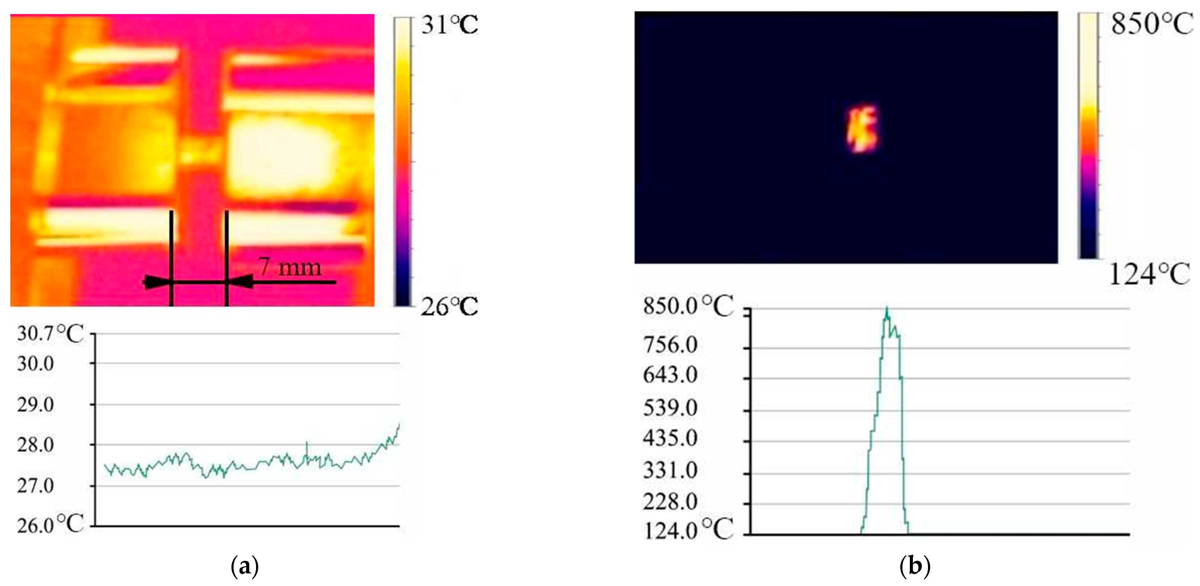
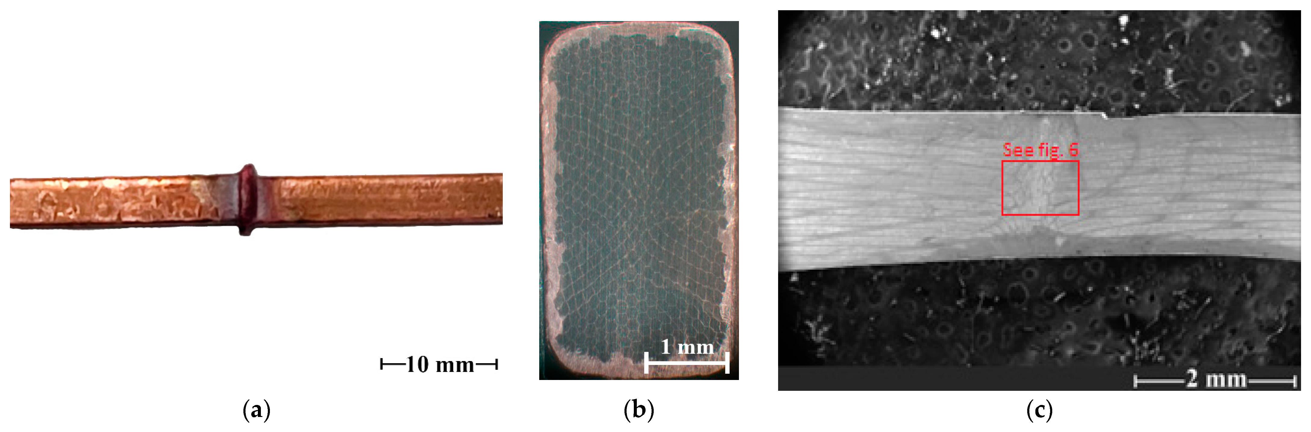
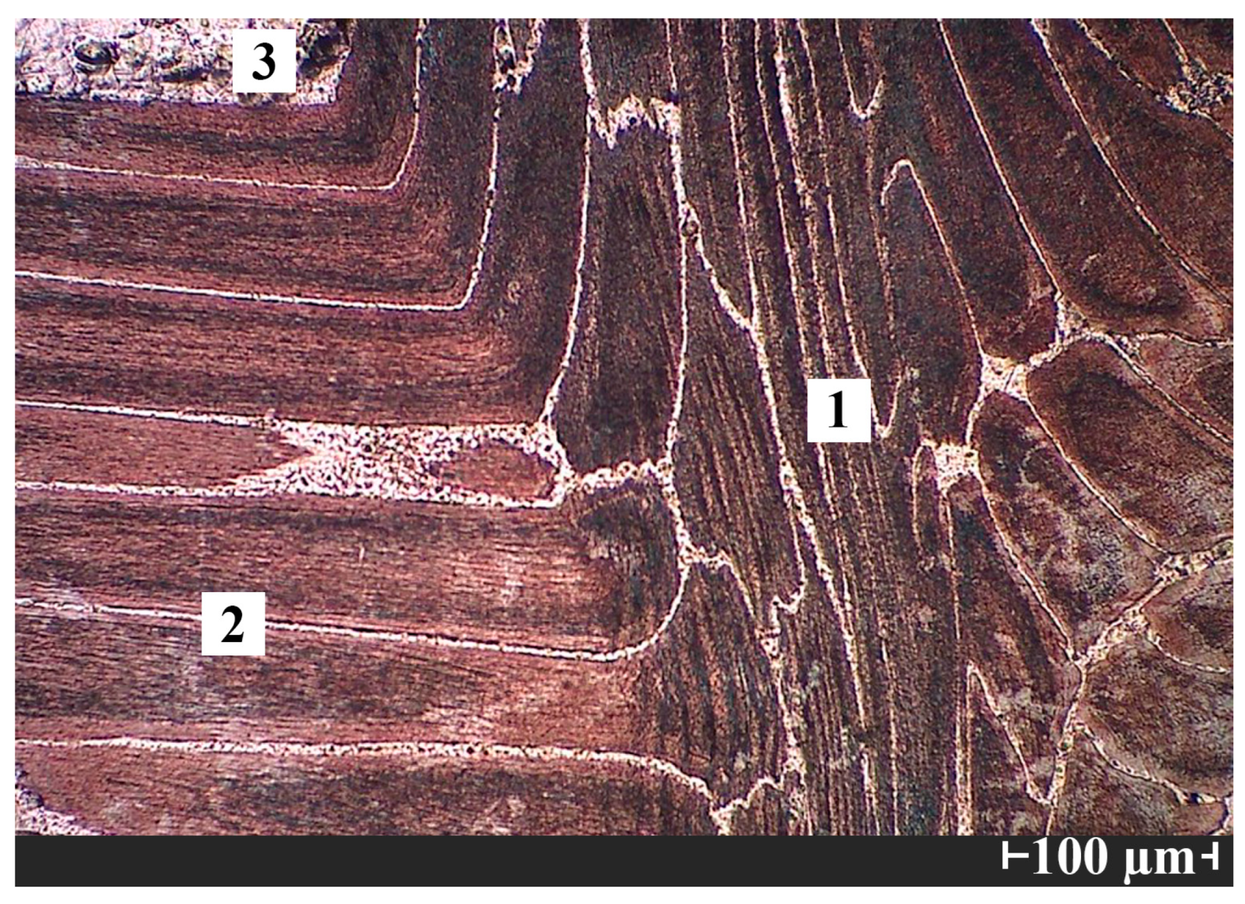
5. Materials, Welding Equipment, Welding Procedures, and Joint Testing Methodology

In this research, a commercially available Cu–Nb (82–18 wt%) microcomposite wire with a rectangular profile and a cross-sectional area of 2.4 × 4.2 mm was used. The wire was manufactured using the assembly deformation method. Its mechanical and physical properties are presented in Table 6.
Different resistance butt welding machines are widely used due to their simplicity and affordability. Many brands, such as IDEAL (Germany), Griggio and Fulgor (Italy), Caika (Ukraine), and other popular models, are available on the European market. The CEA SQ/A121 three-phase AC resistance welding machine (CEA Welding, Lecco, Italy), known for providing higher compression forces (as shown in Table 7), was used for butt welding wire samples.
The temperature of the joining area during welding was observed using the following:
(1) Noncontact infrared Optris Infrared Camera PI450i (Optris IR Sensing, LLC, Portsmouth, NH, USA) with temperature range from −20 till +1500 °C, accuracy ± 2%, resolution 2 °C [59].
(2) Xintest HT-6899 pyrometer (Santa Technology Co., Ltd., Bueng Yitho, Thailand) with spot temperature measurement range from −50 to + 2200 ° C, accuracy ± 2%, resolution 0.1 °C, and response time 0.1 s [60].
Table 7. Technical data of the resistance butt welding machine SQ/A121 [61].
SpecificationsCEA SQ/A121
Welding wire diameter (Cu), mm1.5–20
Supply voltage (AC industrial frequency 50 Hz), V380
Number of phases used, pcs.3
Maximum current of the secondary circuit, A30,000 ± 10%
Voltage of the secondary circuit of the welding transformer, VUp to 5.1
Secondary circuit voltage regulationElectronic
Maximum power at short circuit, kW122
Power at (Duty cycle = 50%), kW25
Maximum welding force, N3500
Maximum upsetting force, N9000
Maximum base length, mm25
Duration of heating (welding), s0.02–2
Upset allowance, mmUp to 5
To evaluate the correctness of the methodology and the results of the optimal welding parameter calculations, an experimental research plan was developed (Table 8). The shielding gas Ar—0.03% NO (EN ISO 14175 [62], Z-Ar+NO-0.03) was used during all welding experiments. The gas was supplied at a flow rate of 10 l/min through a copper pipe with a 10 mm internal diameter.
Four series of welding experiments were planned and conducted on calculations of welding parameters. In each series, specific welding parameters were varied. In the first series, the current intensity (and corresponding current density) and welding time were varied within the limits necessary to achieve desired heating temperatures. Based on quality assessment results of welded joints from this series, a second series was conducted, focusing on electrode distance and welding time. The third series focused on varying upset allowance, while the fourth series examined compression force during welding. Finally, in the fifth series, the variable was the compression force during settlement. In each series, best welding parameters were identified based on visual assessment of joint quality. As a result of the experiments, an optimum welding mode was selected and used for welding all samples that were subsequently analysed for microstructure and joint properties.
The length of the wire samples used for welding was 35 mm. Three specimens were welded under each mode listed in Table 8 to determine the appropriate welding parameters. An additional 15 specimens were welded using the selected optimal welding parameters, which are presented in Table 9.
For electrical resistance measurements, three Cu–Nb wire specimens with butt joints were prepared. Each specimen was 70 cm long, with a 45 mm distance between the measuring contacts. The experiments were conducted according to the methodology outlined in ISO 17279-3:2021 [63]. Electrical resistance was measured using a U2810D digital LCR meter tester (EUCOL, Changzhou, China) [64]. The Joule heating of the specimens by the flow of electric current was observed with a FLIR-E49001 thermal imaging camera (FLIR Systems, Wilsonville, OR, USA) [65]. The samples were electrically heated with 200 A using a welding rectifier (Velga, Vilnius, Lithuania) [66]. The temperature distribution was recorded at the start of the experiment and at 30 s intervals thereafter.
The weld faces were visually inspected using a 10x loupe and higher magnification optical microscopy to identify surface imperfections. Non-destructive tests of the best samples was performed using a GE ERESCO 42MF4 radiographic device (Waygate Technologies, Houston, TX, USA) [67], a Duerr NDT CR 35 NDT scanner (DÜRR NDT GmbH & Co. KG, Bietigheim-Bissingen, Germany) and D-test Viewer version 9.3 digital imaging software [68]. The mechanical properties of the welded joints were determined by tensile testing. Three welded butt joints, each 30 cm in length, were tested. A universal tensile testing instrument, 2055 P-0.5 (Tochpribor, Ivanovo, Russia) [69], equipped with LabVIEW 2020 software (National Instruments, Austin, TX, USA) and PXI system hardware (NI PXIe-1073 chassis and NI PXIe-4330 controller, Austin, TX, USA) [70], was used for testing according to the EN 61788-6:2011 standard [71]. A 10 kN S-type tension load cell (Torbal, Bohemia, NY, USA) [72] and a 3542 extensometer (Epsilon Technology, Jackson, WY, USA) [73] with 25 mm gauge length were used for measurements. Five unmachined specimens (Annex C according ISO EN 6982-1:2019 [74]) were applied in tensile tests. Distance between the grips of machine was 40 mm. Total length of specimens with welded joints was 70 mm.
Butt-welded samples were cross-sectioned to assess weld profile and microstructure. The joint microstructure was analysed using scanning electron microscopy (SEM) and optical microscopy. Specimens for microscopic investigation were prepared by abrasive grinding, diamond polishing, and subsequent electroetching in a solution of 50 mL H₃PO4 and 50 mL H3O. Electrolytic polishing and etching were performed using the PoliMat2 system (Buehler, Lake Bluff, IL, USA) [75], with samples immersed for up to 30 s at approximately 1 V.
An SEM Axia ChemSEM HiVac (Thermo Fisher Scientific, Waltham, MA, USA) [76] equipped with a True Sight X energy dispersive spectrometer (EDS) for chemical microanalysis, and an optical microscope Eclipse MA–200 (Nikon, Tokyo, Japan) [77] with a digital Moticam A16 (Motic, Hong Kong, China) camera [78], were used for microstructure analysis.

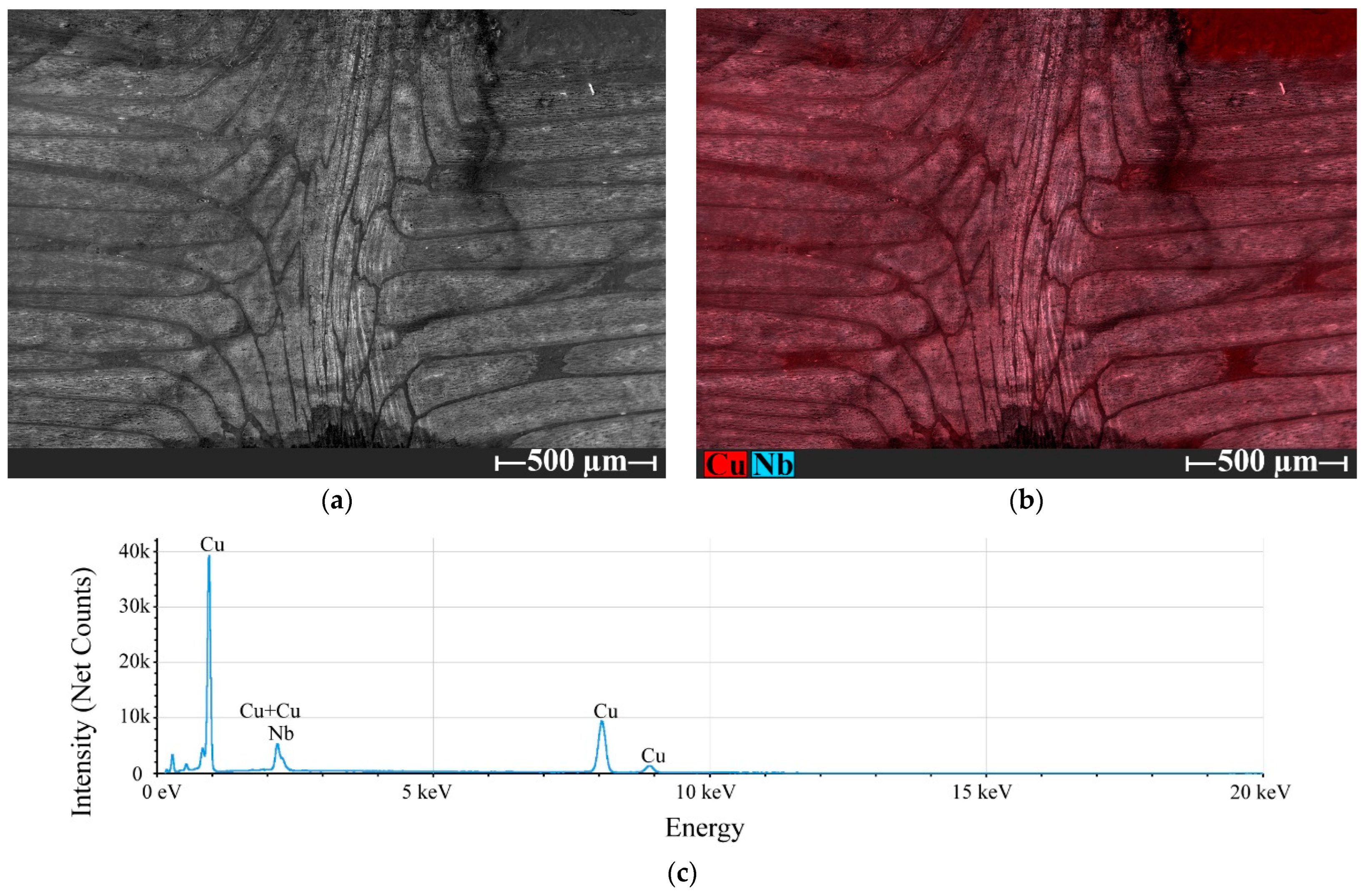
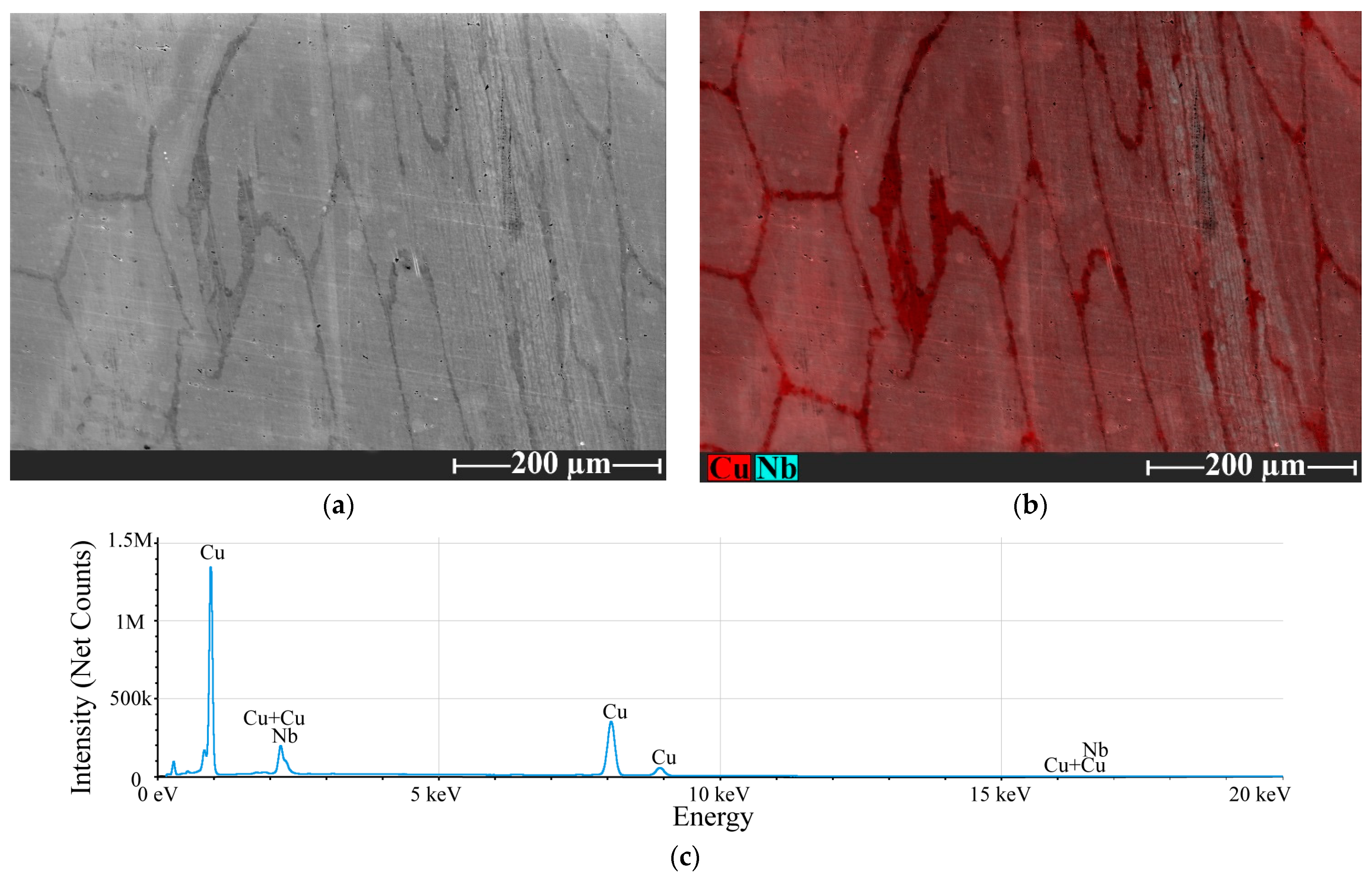
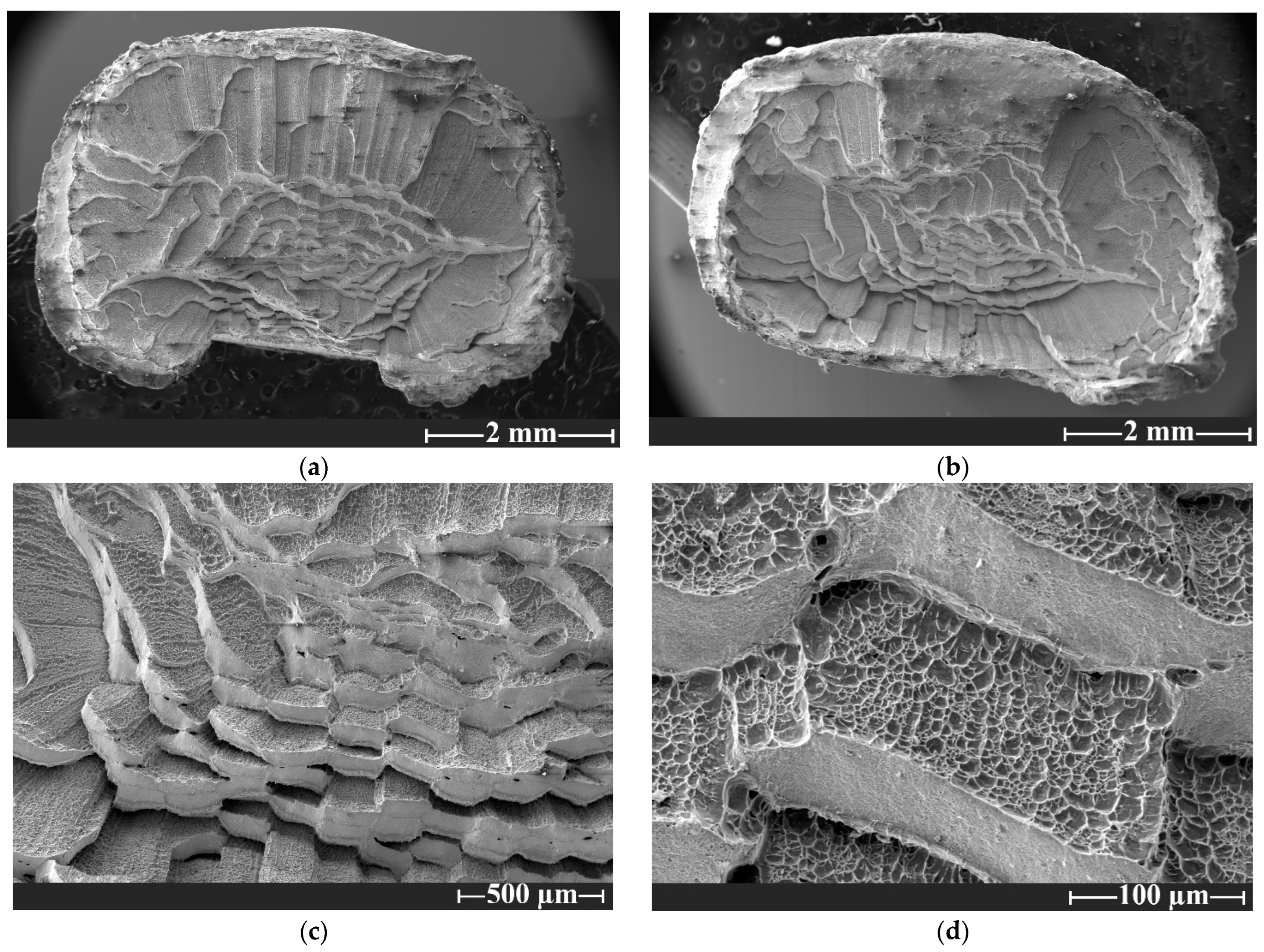
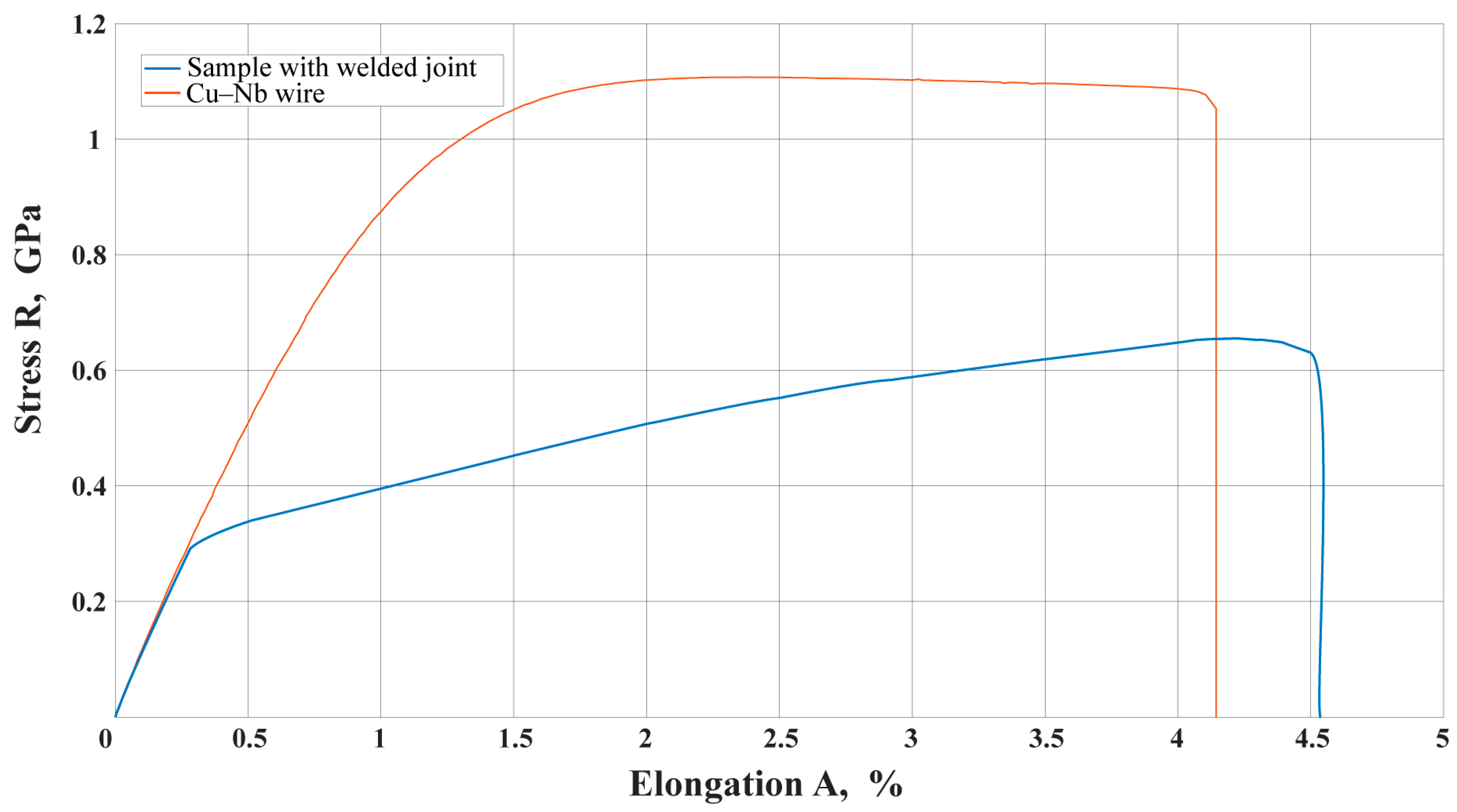
6. Experimental Results and Discussion

The results of the welding tests, based on the experimental design (Table 8), allowed the selection of suitable welding parameters for Cu-Nb conductors according to the quality of joints obtained.
Table 10 presents the results of the experimental welding tests. Both temperature and weld quality are influenced by the combination of current density and welding time. The optimal parameters were determined to be a current density of approximately 267 A/mm2 and a welding time of 0.4 s, which heated the weld zone to 868 °C. Lower current densities resulted in nonwelding, while higher densities caused partial or complete melting of the conductor material or matrix. Two series of experiments identified the most suitable working length, ranging from 6 to 7 mm. Shorter lengths caused joint pegging issues, while longer lengths led to significant bending deformations, misalignment, or slippage of the welded ends. In the fourth series, the optimal precipitation value was found to be between 0.9 and 1 mm. Lower values failed to produce joints, while higher values caused shear or excessive metal extrusion. In the fifth series, the required compression force during welding was determined. Forces exceeding 3500 N (or pressures above 350 MPa) caused severe bending deformation, significant metal extrusion, and shear-type joints. In the final sixth series, an optimal settling force of 4160 N was established, which did not exceed the yield strength of the wire material at the achieved heating temperature (416 MPa).
The optimum welding mode, detailed in Table 9, was used for welding all samples analysed for their properties and microstructure. This mode aligns well with the calculated data.
The maximum heating temperature of the welded joint was determined through non-contact surface temperature measurements. Heating of the samples during the electrical current flow was monitored using a thermal imaging camera and a spot pyrometer. The temperature distributions at the start of the experiment and throughout the welding process are shown in Figure 3.
Maximum surface heating temperature during welding, when electrical current flowed, reached 850 °C. This temperature falls within the recommended range (0.8–0.9 Tm to melting point Tm) and does not exceed the recommended value of 868 °C. Temperature measurement results confirm the accuracy of the upset welding regime calculation methodology and selection of appropriate welding parameters.
To evaluate the mechanical and electrical properties of the joints, several tests were conducted. The electrical properties of the samples with welded joints were compared to those of the conductors without joints by measuring the difference in electrical resistance. A 45 mm conductor without a joint had an electrical resistance of 119.3 µΩ at room temperature. In the conductors with upset resistance welding joints, a slight increase in resistance was observed, with welded samples of the same length showing an electrical resistance of 122.4 µΩ. The difference in electrical resistance between the samples was minimal (approximately 2.5%), which is significant for maintaining performance in electrical contact connections.
Heating of the samples with welded joints during electrical current flow was analysed using a thermal imaging camera. Temperature distributions at the start of the experiment and after 3 min of heating are shown in Figure 3 and Figure 4. The temperature differences between the resistivity welding joints and the conductor during electrical current flow did not exceed the recommended value of 95 °C.
The electrical conductivity of the Cu-Nb conductor was approximately 65.1% IACS. According to various sources, the electrical conductivity of Cu-Nb composite wire can range from 35 to 40 MS/m (60–70% IACS) with a strength of up to 1200 MPa [79,80,81,82]. The calculated electrical conductivity and resistivity values (Table 11) for the Cu-Nb wire are consistent with the data provided by the manufacturer and published in various scientific articles [79,80,81]. The electrical conductivity of the tested samples with upset welded joints reached 63.3% IACS. This measured conductivity is slightly better than that of conductors welded using flash welding.
It was observed that the electrical conductivity of the samples does not change significantly in the presence of a high-quality weld during the measurements of the electrical conductivity of samples with welded joints, which were made using different welding modes. Otherwise, the electrical conductivity of the samples decreases significantly in the presence of very large excessive upset metal, large deformation of the joint zone, misalignment of the edges to be joined or poor bonding of the edges due to excessive deviation of welding parameters from the optimum values (e.g., excessive or too-low welding current, welding and upsetting force).
A general view of the butt welds is shown in Figure 5a. The main criteria for assessing butt weld quality include weld geometry, joint mechanical properties, quantity and size of internal and surface defects, as well as weld microstructure. Quality of obtained upset welding joints was evaluated through nondestructive radiographic tests. No unacceptable internal welding defects (microcracks, cavities, inclusions, or other discontinuities) were observed in digital X-ray images.
The microstructure and form of well-formed butt welds can be observed from the cross-sections of the joints. As shown in Figure 5b and Figure 6, weld joints without cracks, solid inclusions, imperfect shapes, or other imperfections were formed by upset resistance welding. The bonding line of the Cu–Nb wire is clearly visible in the cross-section view.
In the bond area, deformed Nb fibers are visible compared to those in the conductor structure, where fibers are oriented along the composite conductor’s axis. The width of this area with deformed Nb fibers is approximately 1 mm, corresponding to the applied upset allowance. In this case, the characteristic flash welding zone with remelted metal is not observed. As shown in the cross-section view of the butt weld (Figure 5b and Figure 6), no dangerous imperfections typical of upset welding—such as P1700 (hook crack), P401 (no weld), P502 (excessive upset metal), P508 (angular misalignment), P5215 (asymmetrical upset), or P530 (belled joint)—were found, as defined by the EN ISO 6520-1:2007 [83] standard. Significant joint thickening and bending deformation of the composite wire were also practically avoided. This can be attributed to the high strength and stiffness of the Cu-Nb conductor at temperatures near melting [84,85,86,87].
The section of the obtained welded joint shows zones with different microstructures (Figure 4, Figure 5, Figure 6 and Figure 7). Although the microstructure in all joint zones primarily consists of two composite phases—Nb fibers in the Cu matrix—the positive aspect is that no oxides or other undesirable compounds (intermetallic) were found in the joint zone, indicating effective protection in inert gas. The only difference between the weld area structure and the conductor structure is that the conductor microstructure (Zone 1) has a strictly oriented structure, with Nb fibers aligned longitudinally to the conductor axis. In contrast, the bond area (weld) microstructure is composed of substantially deformed fine Nb fibers in the Cu matrix.
Elemental maps for Cu and Nb (Figure 7 and Figure 8, Table 12 and Table 13) show that changes in color shades and spectral analysis data indicate the proportion of copper (80.7 wt%) and niobium (19.3 wt%) in the weld area is very close to the chemical composition of the initial Cu-Nb wire (Table 10). This suggests the weld (bond) was primarily formed through thermal compression of the Cu-Nb conductor. However, due to Cu’s greater ductility, which allows it to be more easily extruded from the fusion line into outer layers (extruded metal—burr), niobium concentration in the fusion line slightly increased (~19.3 wt%). Additionally, as the degree of deformation increases, dislocation density in niobium filaments rises, while copper or bronze matrices undergo deformation softening [88,89,90]. This may contribute to welded joint strength.
The main failure modes in metal matrix composites include fiber fracture, matrix yielding, and splitting caused by debonding at fiber–matrix interfaces or matrix failure [91]. Interfacial debonding between fiber and matrix, fiber bridging when a notch extends into the matrix without fiber fracture, and fiber pull-out also occur. Differences in Young’s modulus and Poisson’s ratio between phases lead to matrix debonding and cracking, further exacerbated by high thermal residual stresses due to mismatched thermal expansion coefficients between the matrix and reinforcement. Additionally, reactions between fibers and the matrix during processing or operation at elevated temperatures pose challenges in metal matrix systems [92]. In elastic matrices, yielding and ductile deformation around fibers can occur, possibly induced by fiber pull-out. The fracture sequence in metal matrix composites often begins with the formation of microcracks in the matrix, typically originating from porosity imperfections, voids, inclusions, or flaws. As these cracks propagate, they approach fibers and deflect along weaker fiber–matrix interfaces, leading to localised rupture of complex bonds [93,94]. SEM images (Figure 9) illustrate the fracture surfaces of the weld area after tensile testing of Cu/Nb composite wire welded samples.
The fracture (through the weld) surfaces of welded samples differ from the brittle character of the breakdown of the composite wire. The images (Figure 9) show that tensile fractures present with a terrace morphology. Such shape of fracture surfaces is closer to ductile fracture case.
No flaws or interfacial debonding were observed in the fractures near the interface regions between Nb filaments and the copper matrix, suggesting excellent bonding due to strong interfaces introduced during wire processing. Figure 9d illustrates fracture surfaces revealing large, deep dimples, indicating a ductile fracture mechanism in the matrix. The fracture surfaces of the Cu matrix are covered with dimples, while Nb fibers show cleavage fracture characteristics, mainly attributed to the different deformability of the Cu matrix and Nb filaments. Based on these observations and Figure 9, it can be concluded that the fracture behavior of Cu-Nb composite welded joints involves microcrack initiation and nucleation in areas deformed during resistance welding. Nb fibers and microcracks easily develop into major cracks in the matrix with increased plastic deformation during tensile testing.
Tensile testing of samples with welded joints shows that all samples fractured through the weld area as expected. The welded connections withstand tensile loads of about 6200 N (Figure 10, Table 14). Consequently, the fracture tensile stress in the area reached 0.62 GPa, which is 55.3% of the tensile strength of the initial microcomposite wire (Figure 10, Table 14). This is a good result compared to the mechanical properties of samples welded by other specialised welding methods published in previous works [3,4,5,6,7,8,9]. The tensile strength obtained in this study is very close to that achieved using the flash welding method. However, the flash welding joints analysed in previous work [9] exhibit lower ductility, with a percentage elongation of about 0.9%, compared to the microcomposite wire and the upset welding joint obtained in this experiment. The percentage of elongation of this connection after fracture was 4.5%. This is about 7% higher than that of the microcomposite wire’s percentage elongation. Therefore, the upset welding joint is less brittle compared to similar joints made by flash welding. The better mechanical properties of the welded joint can be achieved only by using optimal welding modes. Otherwise, the strength and ductility of the samples as well as the electrical conductivity are significantly deteriorated. The mechanical strength and relative elongation of the specimens deteriorate significantly in the presence of excessive upset metal or deformation of the joint zone, misalignment of the edges to be joined, or poor bonding of the edges.

7. Conclusions

The study demonstrated successful butt welds using upset resistance welding for Cu-Nb composite wires. Radiographic tests did not show unacceptable internal welding defects, indicating effective weld formation. The chemical composition in the weld area closely matched that of the original wire, confirming minimal compositional alterations during welding. Weld joints exhibited desirable microstructural characteristics without oxides or undesirable compounds, suggesting effective inert gas protection. Microstructure of the weld area contained deformed Nb fibers within a Cu matrix, differing from conductor structure with its longitudinally aligned fibers. Tensile testing revealed that welded joints withstood significant loads, achieving fracture tensile stress equal to 55.3% of the original wire’s tensile strength. Upset welding joints exhibited higher ductility than those produced by alternative welding methods, such as flash welding. SEM analysis indicated fractures in the weld area showed large dimples, characteristic of ductile fracture mechanisms, and cleavage features in Nb fibers. This behavior was attributed to plastic deformation during tensile testing and strong fiber–matrix bonding introduced during processing. Mechanical properties and fracture characteristics of upset welded joints were favorable compared to those achieved by other welding methods, particularly due to improved ductility and reduced brittleness compared with flash welding. In summary, findings underscore the efficacy of upset resistance welding for Cu-Nb composite wires, offering a balance between strength and ductility, making it a viable technique for conductors’ nondestructive joining. Moreover, the heat-affected zone is also narrow, and the heating temperature is lower than the melting temperature of the composite. Therefore, welding occurs in the solid phase without the remelt of a Cu-Nb composite.
Thus, upset welding technology, in principle, is applicable to electrical contact connections with Cu-Nb microcomposite wire. Obviously, the tensile strength of such welded joint is two times lower than that of the composite wire and therefore cannot withstand the maximum loads that this composite conductor can withstand. Therefore, such welded joints cannot be applied inside of solenoids for windings connection. But the upset welding joints are suitable for use in solenoid terminal connections with external electrical circuits that are not directly exposed to high magnetic or tensile forces that are generated inside a solenoid of a pulsed magnet system.

Author Contributions

Conceptualisation, N.V. and P.B.; formal analysis, N.V. and P.B.; investigation, P.B. and O.K.; methodology, N.V.; resources, N.V. and O.K.; writing—original draft preparation, P.B., O.K. and N.V.; writing—review and editing, N.V., P.B. and O.K.; visualisation, O.K. All authors have read and agreed to the published version of the manuscript.

Funding

This research received no external funding.

Institutional Review Board Statement

Not applicable.

Informed Consent Statement

Not applicable.

Data Availability Statement

The original contributions presented in the study are included in the article; further inquiries can be directed to the corresponding author.

Conflicts of Interest

The authors declare no conflicts of interest.

Abbreviations

The following abbreviations are used in this manuscript:
TWThermite welding
LWLaser welding
EBWElectron beam welding
ERWElectric resistance welding

References

  1. Shikov, A.K.; Pantsyrnyi, V.I.; Vorob’Eva, A.E.; Sud’Ev, S.V.; Khlebova, N.E.; Silaev, A.K.; Belyakov, N.A. Copper-Niobium High Strength and High Conductivity Winding Wires for Pulsed Magnets. Mater. Sci. Heat Treat. 2002, 44, 491–495. [Google Scholar]
  2. Głuchowski, W.; Rdzawski, Z.; Stobrawa, J.P.; Marszowski, K.J. Microstructure and Properties of Cu-Nb Wire Composites. Arch. Metall. Mater. 2014, 59, 35–40. [Google Scholar] [CrossRef]
  3. Višniakov, N.; Mikalauskas, G.; Černašėjus, O.; Škamat, J. Laser Welding of Copper-Niobium Microcomposite Wires for Pulsed Power Applications. Mater. Sci. Eng. Technol. 2019, 50, 646–662. [Google Scholar] [CrossRef]
  4. Višniakov, N.; Mikalauskas, G.; Černašėjienė, R.; Škamat, J.; Černašėjus, O.; Novickij, V. Feasibility Evaluation of Cu-Nb Microcomposite Joints Formed by Magnetic Field Pressing for Pulsed Power Applications. Teh. Vjesn. 2018, 25 (Suppl. S2), 326–329. [Google Scholar] [CrossRef]
  5. Višniakov, N.; Mikalauskas, G.; Černašėjienė, R.; Černašėjus, O.; Škamat, J. Electron beam welding of copper-niobium microcomposites for pulsed power applications. Mater. Sci. Eng. Technol. 2018, 49, 538–550. [Google Scholar] [CrossRef]
  6. Višniakov, N.; Mikalauskas, G.; Škamat, J.; Černašėjienė, R.; Černašėjus, O.; Rudzinskas, V.; Boris, R. Thermite welding of Cu–Nb microcomposite wires. Int. J. Mater. Res. 2017, 108, 832–839. [Google Scholar] [CrossRef]
  7. Mikalauskas, G. Investigation of Welded Joints and Weldability of Microcomposite Copper-Niobium Conductors for the Application in High Magnetic Field Systems. Ph.D. Dissertation, Vilnius Gediminas Technical University, Vilnius, Lithuania, 2020; p. 122. (In Lithuanian). Available online: http://dspace.vgtu.lt/handle/1/3838 (accessed on 11 February 2025).
  8. Višniakov, N.; Novickij, J.; Ščekaturovienė, D.; Petrauskas, A. Quality Analysis of Welded and Soldered Joints of Cu-Nb Microcomposite Wires. In Proceedings of the National Conference on Materials Engineering, Kaunas, Lithuania, 19 November 2010; Technologija: Kaunas, Lithuania, 2011; Volume 17, pp. 16–19. [Google Scholar] [CrossRef]
  9. Višniakov, N.; Škamat, J.; Černašėjus, O.; Kilikevičius, A. Flash welding of microcomposite wires for pulsed power applications. Metals 2020, 10, 1053. [Google Scholar] [CrossRef]
  10. ISO 17279-1:2018; Welding—Micro Joining of 2nd Generation High Temperature Superconductors—Part 1: General Requirements for the Procedure. International Organization for Standardization: Geneva, Switzerland, 2018.
  11. Paul, H.; Miszczyk, M.; Prażmowski, M.; Chulist, R.; Petrzak, P.; Schell, N.; Fatemi, M. Effect of Impact Loading on Structural Properties of Multi-Layered Ta/Cu, Nb/Cu and Fe/Cu Plates Fabricated by Single-Shot Explosive Welding. IOP Conf. Ser. Mater. Sci. Eng. 2022, 1270, 012124. [Google Scholar] [CrossRef]
  12. Beinoras, P.; Mikalauskas, G.; Višniakov, N.; Kapustynskyi, P. Comparative Analysis of Cu-Nb Microcomposite Conductor Welding Techniques. In Proceedings of the International Conference on Metallurgy and Materials (METAL), Brno, Czech Republic, 22–24 May 2024; pp. 269–274. [Google Scholar] [CrossRef]
  13. Kanne, W.R., Jr. Solid-State Resistance Upset Welding: A Process with Unique Advantages for Advanced Materials; Westinghouse Savannah River Co.: Aiken, SC, USA, 1993. [Google Scholar]
  14. Messler, R.W. Joining of Advanced Materials; Butterworth-Heinemann: Oxford, UK, 2013; p. 560. [Google Scholar]
  15. O’Brien, A. Welding Handbook. Volume 3, Welding Processes, Part 2, 9th ed.; American Welding Society: Miami, FL, USA, 2007; p. 615. [Google Scholar]
  16. Campbell, F.C. Joining: Understanding the Basics; Resistance Welding; ASM International: Materials Park, OH, USA, 2011; Chapter 3; p. 322. [Google Scholar] [CrossRef]
  17. Kanne, W.R., Jr. Welding, Brazing, and Soldering; Upset Welding; ASM Handbook; ASM International: Materials Park, OH, USA, 1993; Volume 6, pp. 249–251. [Google Scholar] [CrossRef]
  18. Gelman, A.S. Fundamentals of Pressure Welding; Mashinostroenie: Moscow, Russia, 1970; p. 302. (In Russian) [Google Scholar]
  19. Weman, K. Welding Processes Handbook, 2nd ed.; Woodhead Publishing Limited: Cambridge, UK, 2012; pp. 119–132. [Google Scholar]
  20. Guo, J. Handbook of Manufacturing Engineering and Technology. Solid State Welding Processes in Manufacturing; Springer: London, UK, 2015; pp. 569–592. [Google Scholar] [CrossRef]
  21. Tierney, J.J.; Gillespie, J.W.; Bourban, P.E. Joining of Composites. In Comprehensive Composite Materials; Materials Science and Materials Engineering; Elsevier: Amsterdam, The Netherlands, 2000; Volume 2, pp. 1029–1047. [Google Scholar] [CrossRef]
  22. Pfeifer, M. Manufacturing Process Considerations. In Materials Enabled Designs, 1st ed.; Butterworth-Heinemann: Oxford, UK, 2009; pp. 115–160. [Google Scholar] [CrossRef]
  23. Kerstens, N.F.H.; Richardson, I.M. Heat distribution in resistance upset butt welding. J. Mater. Process. Technol. 2009, 209, 2715–2722. [Google Scholar] [CrossRef]
  24. Lienert, T.; Siewert, T.; Babu, S.; Acoff, V. ASM Handbook, Welding Fundamentals and Processes; ASM International: Materials Park, OH, USA, 2011; Volume 6A. [Google Scholar] [CrossRef]
  25. Russell, J.D. The potential use of non-arc welding processes in energy-related fabrications. In Welding in Energy-Related Projects; Welding Institute of Canada: Windsor, ON, Canada; Pergamon Press: Toronto, ON, Canada, 1984; p. 491. [Google Scholar]
  26. Hook, I.T. The Welding of Copper and Its Alloys. Weld. J. 1955, 34, 177S–202S. [Google Scholar]
  27. Davis, J.R. ASM Specialty Handbook: Copper and Copper Alloys; ASM International: Materials Park, OH, USA, 2008; p. 621. [Google Scholar]
  28. Somers, B.R. Welding Handbook, 8th ed.; Welding of Copper and Copper Alloys; American Welding Society: Miami, FL, USA, 1997; Volume 3, p. 54. [Google Scholar]
  29. Kearns, W.H. Welding Handbook, 7th ed.; Metals and Their Weldability; American Welding Society: Miami, FL, USA, 1982; Volume 4, p. 561. [Google Scholar]
  30. Columbic Copper Reinforced Wires, Conductors & Wire Rod. Nanoelectro Superwires. Available online: https://www.monrf.ru/upload/iblock/31d/31dab85e9b572a77e4e70c0ae60ae892.pdf (accessed on 10 February 2025).
  31. Cu-Nb Phase Diagram. Springer Materials. Available online: https://link.springer.com/article/10.1007/s11669-012-0051-y (accessed on 10 February 2025).
  32. Hust, J.G.; Sparks, L.L. Lorenz Ratios of Technically Important Metals and Alloys; Technical Note 634; National Bureau of Standards: Washington, DC, USA, 1973; p. 276. Available online: https://nvlpubs.nist.gov/nistpubs/Legacy/TN/nbstechnicalnote634.pdf (accessed on 10 February 2025).
  33. ISO/TR 25901-3:2016; Welding and Allied Processes—Vocabulary—Part 3: Welding Processes. International Organization for Standardization: Geneva, Switzerland, 2016.
  34. Kochergin, K.A. Resistance Welding; Mashinostroenie: Moscow, Russia, 1987; p. 240. (In Russian) [Google Scholar]
  35. Katayev, R.F.; Milyutin, V.S.; Bliznik, M.G. Theory and Technology of Resistance Welding; Ural State University: Yekaterinburg, Russia, 2015; p. 144. (In Russian) [Google Scholar]
  36. ISO 4063:2009; Welding and Allied Processes—Nomenclature of Processes and Reference Numbers. International Organization for Standardization: Geneva, Switzerland, 2009.
  37. Ababkov, N.V.; Pimonov, M.V. Technology and Equipment of Resistance Welding; Kuzbass State Technical University: Kemerovo, Russia, 2011; p. 258. (In Russian) [Google Scholar]
  38. Glebov, L.V.; Filippov, J.I.; Chiuloshnikov, P.P. Design and Exploitation of Resistance Machines; Energoizdat: Leningrad, Russia, 1987; p. 312. (In Russian) [Google Scholar]
  39. AWS C1.1M/C1.1:2012; Recommended Practices for Resistance Welding. American Welding Society: Miami, FL, USA, 2012.
  40. American Welding Society. RWMA Resistance Welding Manual, 4th ed.; American Welding Society: Miami, FL, USA, 2003. [Google Scholar]
  41. Orlov, B.D. Technology and Equipment for Resistance Welding; Mashinostroenie: Moscow, Russia, 1986; p. 352. (In Russian) [Google Scholar]
  42. Banov, M.D. Technology and Equipment for Resistance Welding, 3rd ed.; Akademiya: Moscow, Russia, 2008; p. 224. (In Russian) [Google Scholar]
  43. Gelman, A.S. Technology of Electric Resistance Welding; Mashinostroenie: Moscow, Russia, 1952; p. 322. (In Russian) [Google Scholar]
  44. Sergeev, N.P. Handbook for Young Welders with Resistance Machines; Vishaya Shkola: Moscow, Russia, 1984; p. 157. (In Russian) [Google Scholar]
  45. Gulyaev, A.I. Technology and Equipment for Resistance Welding; Mashinostroenie: Moscow, Russia, 1985; p. 256. (In Russian) [Google Scholar]
  46. Vural, M. Comprehensive Materials Processing; Welding Processes and Technologies; Elsevier: Amsterdam, The Netherlands, 2014; Volume 6, pp. 3–48. [Google Scholar] [CrossRef]
  47. Ovchinnikov, V.; Gureeva, M. Technology and Equipment for Resistance Welding: Handbook; Infra-Inzhenerija: Moscow, Russia, 2020; p. 160. (In Russian) [Google Scholar]
  48. American Welding Society. RWPH:2011 Resistance Welding Pocket Handbook, 1st ed.; American Welding Society: Miami, FL, USA, 2011; p. 45. [Google Scholar]
  49. Zhang, H.; Senkara, J. Resistance Welding: Fundamentals and Applications, 2nd ed.; CRC Press: Boca Raton, FL, USA, 2017; p. 427. [Google Scholar]
  50. Fang, Y.; Jiang, X.; Mo, D.; Zhu, D.; Luo, Z. A Review on Dissimilar Metals’ Welding Methods and Mechanisms with Interlayer. Int. J. Adv. Manuf. Technol. 2019, 102, 2845–2863. [Google Scholar] [CrossRef]
  51. Martinsen, K.; Hu, S.J.; Carlson, B.E. Joining of Dissimilar Materials. CIRP Ann.—Manuf. Technol. 2015, 64, 679–699. [Google Scholar] [CrossRef]
  52. ISO/TR 23413:2019; Resistance Welding—Overview of Standards for Resistance Welding. International Organization for Standardization: Geneva, Switzerland; Beijing, China, 2019.
  53. Devanathan, V. The Wiedemann-Franz Law for Electrical and Thermal Conduction in Metals. J. Chennai Acad. Sci. 2021, 4, 1–26. [Google Scholar]
  54. Solovjev, G.I. Fundamentals of Technology of Pressure Vessel; Kurgan State University: Kurgan, Russia, 2014; p. 40. (In Russian) [Google Scholar]
  55. Gomez, M.R.; French, D.M.; Tang, W.; Zhang, P.; Lau, Y.Y.; Gilgenbach, R.M. Experimental Validation of a Higher Dimensional Theory of Electrical Contact Resistance. Appl. Phys. Lett. 2009, 95, 071501. [Google Scholar] [CrossRef]
  56. Hamedi, M.; Atashparva, M. A Review of Electrical Contact Resistance Modeling in Resistance Spot Welding. Weld. World 2017, 61, 269–290. [Google Scholar] [CrossRef]
  57. Qi, A.; Yang, W.; Liu, B.; Zheng, S. Interface Effects on the Properties of Cu–Nb Nanolayered Composites. J. Mater. Res. 2020, 35, 2684–2700. [Google Scholar] [CrossRef]
  58. Hashemi, N.; Vazir, H.; Ziemer, K. Wear Resistance of Cu–18vol.% Nb (P/M) Composites. Mater. Sci. Eng. A 2008, 478, 390–396. [Google Scholar] [CrossRef]
  59. Optris PI 450i Infrared Camera. Optris GmbH. Available online: https://optris.com/products/infrared-cameras/precision-line/pi-450i (accessed on 11 February 2025).
  60. XINTEST HT-6899 Non-Contact High Temperature Infrared Thermometer Datasheet. Santa Technology. Available online: https://santatechnology.com/products-datasheet/8341-1628154065.pdf (accessed on 11 February 2025).
  61. SQ-AS Welding Wire. CEA Welding. Available online: https://www.ceaweld.com/en/product/sq-as (accessed on 11 February 2025).
  62. ISO 14175:2008; Welding Consumables—Gases and Gas Mixtures for Fusion Welding and Allied Processes. International Organization for Standardization: Geneva, Switzerland, 2008.
  63. ISO 17279-3:2021; Welding—Micro Joining of Second Generation High Temperature Superconductors—Part 3: Test Methods for Joints. International Organization for Standardization: Geneva, Switzerland, 2021.
  64. Changzhou Eucol Electronic Technology Co., Ltd. Available online: http://www.en.eucol.com.cn (accessed on 11 February 2025).
  65. FLIR Exx-Series Advanced Thermal Imaging Cameras. FLIR Systems. Available online: https://www.flir.com/instruments/exx-series (accessed on 11 February 2025).
  66. VELGA VILNIUS. Available online: https://www.velga.lt (accessed on 11 February 2025).
  67. ERESCO 42 MF4 Portable X-Ray Unit Brochure. GE Sensing & Inspection Technologies. Available online: https://pratita.com/wp-content/uploads/2020/04/eresco_42_mf4_air-cooled_brochure_english-pdf.pdf (accessed on 11 February 2025).
  68. HD-CR 35 NDT. Dürr NDT GmbH. Available online: https://www.duerr-ndt.de/produkte/computer-radiographie/hd-cr-35-ndt.html (accessed on 11 February 2025).
  69. JSC Tochpribor. Available online: https://www.tochpribor-kb.ru (accessed on 11 February 2025).
  70. PXIe-1073. National Instruments. Available online: https://www.ni.com/en-us/shop/model/pxie-1073.html (accessed on 11 February 2025).
  71. EN 61788-6:2011; Superconductivity—Mechanical Properties Measurement. Room Temperature Tensile Test of Cu/Nb-Ti Composite Superconductors. European Committee for Electrotechnical Standardization: Brussels, Belgium, 2011.
  72. 10kN Load Cell. Torbal Scales. Available online: https://www.torbalscales.com/10kn-load-cell.html (accessed on 11 February 2025).
  73. Axial Extensometer—Model 3542. Epsilon Technology Corp. Available online: https://www.epsilontech.com/products/axial-extensometer-model-3542 (accessed on 11 February 2025).
  74. ISO 6892-1:2019; Metallic Materials—Tensile Testing—Part 1: Method of Test at Room Temperature. Lietuvos Standartizacijos Departamentas: Vilnius, Lithuania, 2020.
  75. PoliMat® 2 Electropolishing and Etching System. Buehler. Available online: https://www.buehler.com/products/grinding-and-polishing/electropolishing-and-etching/polimat-2-electropolishing-and-etching-system/ (accessed on 11 February 2025).
  76. Axia ChemiSEM. Thermo Fisher Scientific. Available online: https://www.thermofisher.com/lt/en/home/electron-microscopy/products/scanning-electron-microscopes/axia-chemisem (accessed on 11 February 2025).
  77. Inverted Eclipse MA200. Nikon Instruments Inc. Available online: https://industry.nikon.com/en-us/products/industrial-microscopy/industrial-microscopes/inverted-eclipse-ma200 (accessed on 11 February 2025).
  78. Moticam A16. Motic Europe. Available online: https://moticeurope.com/en/moticam-a16.html (accessed on 11 February 2025).
  79. Blaschke, D.N.; Miller, C.; Mier, R.; Osborn, C.; Thomas, S.M.; Tegtmeier, E.L.; Winter, W.P.; Carpenter, J.S.; Hunter, A. Predicting Electrical Conductivity in Cu/Nb Composites: A Combined Model-Experiment Study. J. Appl. Phys. 2022, 132, 045105. [Google Scholar] [CrossRef]
  80. Mao, Q.; Wang, L.; Nie, J.F.; Zhao, Y. Enhancing Strength and Electrical Conductivity of Cu–Cr Composite Wire by Two-Stage Rotary Swaging and Aging Treatments. Compos. Part B Eng. 2022, 231, 109567. [Google Scholar] [CrossRef]
  81. High Strength, High Conductivity Nanocomposite Cu-Nb Wires. Alphysica. Available online: https://alphysica.rhymedigital.com/cu-nb.html (accessed on 11 February 2025).
  82. Beinoras, P.; Višniakov, N. Measurement of Electrical Conductivity and Resistivity of Cu-Nb18% Microcomposite Conductor and Its Welded Joint. Sci. Future Lith. 2024, 16, 1–8. (In Lithuanian) [Google Scholar] [CrossRef]
  83. ISO 6520-1:2007; Welding and Allied Processes—Classification of Geometric Imperfections in Metallic Materials—Part 1: Fusion Welding. International Organization for Standardization: Geneva, Switzerland, 2007.
  84. De Almeida, R.; De Aguiar, J.; Passos, C. Investigating the “Cocoon Effect” in Niobium-Copper Alloy: Metallic Nano-Precipitate Distribution and Niobium Migration. arXiv 2024, arXiv:2309.06385. [Google Scholar] [CrossRef]
  85. Deng, L.; Han, K.; Wang, B.; Yang, X.; Liu, Q. Thermal Stability of Cu–Nb Microcomposite Wires. Acta Mater. 2015, 101, 181–188. [Google Scholar] [CrossRef]
  86. Yang, W.; Beyerlein, I.J.; Jin, Q.; Ge, H.; Xiong, T.; Yang, L.; Pang, J.; Zhou, Y.; Shao, X.; Zhang, B.; et al. Strength and Ductility of Bulk Cu/Nb Nanolaminates Exposed to Extremely High Temperatures. Scripta Mater. 2019, 166, 73–77. [Google Scholar] [CrossRef]
  87. Spitzig, W.; Krotz, P.; Chumbley, L.S.; Downing, H.; Verhoeven, J. Effect of Temperature on the Mechanical Properties and Microstructures of In Situ Formed Cu-Nb and Cu-Ta Composites. MRS Proc. 2011, 120, 45. [Google Scholar] [CrossRef]
  88. Popova, E.N.; Sudareva, S.V.; Popov, V.V.; Rodionova, L.A.; Romanov, E.P.; Vorob’eva, A.E.; Dergunova, E.A.; Malafeeva, O.V.; Khlebova, N.E.; Shikov, A.K. Plastic Deformation of Composites Cu/Nb, Cu/Nb(Ti) and Cu-Sn/Nb(NbTi). Fiz. Met. Metalloved. 2001, 90, 115–124. (In Russian) [Google Scholar]
  89. Popova, E.N.; Popov, V.; Romanov, E.P.; Pilyugin, V.P. Effect of the Degree of Deformation on the Structure and Thermal Stability of Nanocrystalline Niobium Produced by High-Pressure Torsion. Phys. Met. Metallogr. 2007, 103, 407–413. [Google Scholar] [CrossRef]
  90. Popova, E.N.; Deryagina, I.L.; Valova-Zaharevskaya, E.G.; Ruello, M.L.; Popov, V.V., Jr. Microstructural Features in Multicore Cu-Nb Composites. Materials 2021, 14, 7033. [Google Scholar] [CrossRef]
  91. Ananth, C.R.; Voleti, S.R.; Chandra, N. Effect of Fiber Fracture and Interfacial Debonding on the Evolution of Damage in Metal Matrix Composites. Compos. Part A Appl. Sci. Manuf. 1998, 29, 1203–1211. [Google Scholar] [CrossRef]
  92. King, J.E. Failure in Composite Materials. Met. Mater. 1989, 5, 720–726. [Google Scholar]
  93. Nickolas, T.; Ahmad, J. Modeling Fiber Breakage in a Metal-Matrix Composite. Compos. Sci. Technol. 1994, 52, 29–38. [Google Scholar] [CrossRef]
  94. Xia, Z.; Curtin, W.A.; Peters, P.W.M. Multiscale Modeling of Failure in Metal Matrix Composites. Acta Mater. 2001, 49, 273–284. [Google Scholar] [CrossRef]
Figure 1. Diagram of the resistance welding process modes: ts—squeeze time; Iw—welding current; tw—parts heating (welding) time; tu—upsetting time; Δu—upset allowance, mm; Fw—welding force; Fu—upsetting force. The abbreviations on Y-axis: F—force; I—current; T—temperature; Δ—allowance. The abbreviations on X axis: t—time.
Metals 15 00394 g001
Figure 2. Diagram for selecting upset welding parameters.
Metals 15 00394 g002
Figure 3. The heating temperature measurement during upset resistance welding: (a) thermal image obtained before welding start; (b) thermal image obtained during welding process.
Metals 15 00394 g003
Figure 4. Distribution of the temperature in the specimen after 3 min of 200 A current flow: (a) main view; (b) enlarged view; 1, 2—measurement points in the joint area.
Metals 15 00394 g004
Figure 5. General view of Cu–Nb wire butt joint after resistance welding: (a) top view (×3 magnification); (b) transverse cross-section of Cu-Nb conductor (×63 magnification); (c) longitudinal cross-section view (×63 magnification).
Metals 15 00394 g005
Figure 6. Microstructure of a butt joint (longitudinal cross-section): enlarged area highlighted in Figure 5b; 1—weld interface with deformed Nb ribbons; 2—Cu–Nb conductor wire with longitudinally oriented Nb ribbons; 3—Cu core.
Metals 15 00394 g006
Figure 7. Structure of a welded joint (SEM and EDS analysis): (a) weld interface microstructure (×200 magnification); (b) Cu and Nb element distribution map in joint area; (c) EDS spectrum of elements in conductor material.
Metals 15 00394 g007
Figure 8. Structure of a welded joint (SEM and EDS analysis): (a) Enlarged microstructure of weld area (×650 magnification); (b) Cu and Nb element distribution map in weld area; (c) EDS spectrum of elements in conductor material.
Metals 15 00394 g008
Figure 9. Fracture surface of joint broken under tension: (a) ×63; (b) ×63; (c) ×250; (d) ×1200.
Metals 15 00394 g009
Figure 10. Tensile stress–percentage elongation curves.
Metals 15 00394 g010
Table 1. Melting points of pure metals and metal composites [30].
Melting Temperature of Cu MatrixMelting Temperature of Nb Reinforcement PhaseMelting Temperature of Cu-18 wt. % Nb Composite
Tm, (Cu) °CTm, (Nb) °CTm, (Cu-Nb) °C
108524691675–1800
Table 2. Physical properties of Cu-18 wt. % Nb composites [30,31,32].
Electrical Resistivity ρo at Room Temperature,
µΩ cm
Electrical Resistivity ρt at Temperature Near Melting,
µΩ cm
Relative Thermal Conductivity
Kt
Electrical Conductivity
IACS, %
Lorenz Number
L, 10−8 · W · Ω/°K2
2.30–2.8718.86–23.530.7560–752.4–2.54
Electrical conductivity,
σ, Ω−1 cm−1
Conductor Density
γ, g/cm3
Specific heat
c, J/kg °C
(cal/g °C)
Thermal conductivity coefficient
λ, W/m °C
(cal/ cm s °C)
Thermal diffusivity,
a, mm2/s
0.348–0.4358.882381
(0.09100033)
401
(0.958413002)
118.5
Table 3. Results of the calculation of the dimensions and compression parameters of a welded joint.
Welding Pressure
Pw, MPa
Upsetting Pressure
Pu, MPa
Welding Force
Fw, N
Upsetting Force
Fd, N
Minimum Basic Length
l0, mm
Upset Allowance
Δu, mm
Heating Temperature
T, °C
350430350043007–10.70.7–1.1868–1085
Table 4. Results of the resistance welding circuit resistance calculation.
Contact Resistance Between Connecting Surfaces
Rc, µΩ
Specific Resistance of the Metal of the Parts That Are Being Welded at the Beginning of the Process
2Rd1, µΩ
Specific Resistance of the Metal of the Welded Parts at the End of the Process
2Rd2, µΩ
Total Resistance of the Welding Circuit at the Beginning of the Process
R1, µΩ
Total Resistance of the Welding Circuit at the End of the Process
R2, µΩ
Calculated Average Loop Resistance
R, µΩ
1.3118.148.619.4148.634
Table 5. Results of the calculation of electrical parameters of resistance welding and welding duration.
Welding Current Density
J, A/mm2
Welding Time
tw, s
Heating Up to T = 868 °C
Requires a Welding Current
Iw, A
Heating Up to T = 977 °C
Requires a Welding Current
Iw, A
Heating Up to T = 1085 °C
Requires a Welding Current
Iw, A
335–37430.25334835523743
307–3420.3306732533428
285–3180.35284630203182
267–2980.4266928312983
252–2820.45252026742817
240–2680.5239525402677
229–2560.55228624252556
Where bold text—optimal welding parameters.
Table 6. Profile and properties of copper–niobium wire [1,2,30,58].
Rectangular Profile Size,
mm × mm
Cross-Section
S, cm2
Yield Strength
σγ, MPa
Ultimate Tensile Strength
σu, MPa
Elongation After Fracture
A, %
Electrical Conductivity
IACS, %
2.4 × 4.20.183011204.260–70
Table 8. The following welding parameters were used for butt resistance welding.
Set of ExperimentsWelding Current
I, A
Welding Current Density
A/mm2
Welding Force
N
Upsetting Force
N
Base Length
mm
Upset Allowance
mm
Welding Time
s
Achieved Welding Temperature
T, °C
A.1284628535004300710.35868
A.23020302977
A.331823181085
A.426692670.4868
A.52831283977
A.629832981085
A.725202520.45868
A.82674267977
A.928172821085
L.1284628535004300610.35868
L.228462858
L.328462859
L.4284628510
L.5266926760.4
L.626692678
L.726692679
L.8266926710
L.9252025260.45
L.1025202528
L.1125202529
L.12252025210
Δ.128462853500430070.70.35868
Δ.226692670.4
Δ.325202520.45
Δ.428462850.80.35
Δ.526692670.4
Δ.625202520.45
Δ.728462850.90.35
Δ.826692670.4
Δ.925202520.45
Δ.1028462851.10.35
Δ.1126692670.4
Δ.1225202520.45
F.1284628541604300710.35868
F.226692670.4
F.325202520.45
F.4284628546800.35
F.526692670.4
F.625202520.45
U.12846285350041600.35
U.226692670.4
U.325202520.45
U.4284628546800.35
U.526692670.4
U.625202520.45
Where bold text—optimal welding parameters.
Table 9. Optimal parameters for butt resistance welding of Cu–Nb wire samples.
Welding Current
I, A
Welding Current Density
A/mm2
Welding Force
Fw, N
Upsetting Force
Fd, N
Base Length
l0, mm
Upset Allowance
Δu, mm
Welding Time, sAchieved Welding Temperature
T, °C
267026735004300710.4868
Table 10. Butt resistance welding parameters.
Set of experimentsA.1A.2A.3A.4A.5A.6A.7A.8A.9
Welding qualitypoorpoorpoorgoodpoorpoorno *poorpoor
Set of experimentsL.1L.2L.3L.4L.5L.6L.7L.8L.9
Welding qualitypoorpoorpoorno *goodpoorno *nono
Set of experimentsL.10L.11L.12Δ.1Δ.2Δ.3Δ.4Δ.5Δ.6
Welding qualityno *no *no *no *no *no *poorpoorno *
Set of experimentsΔ.7Δ.8Δ.9Δ.10Δ.11Δ.12F.1F.2F.3
Welding qualitypoorgoodno *poorpoorno *poorpoorno *
Set of experimentsF.4F.5F.6U.1U.2U.3U.4U.5U.6
Welding qualitypoorpoorno *poorgoodno *poorpoorno *
Where no *—no weld obtained. And where bold text—optimal welding parameters.
Table 11. Electrical resistivity and conductivity for butt upset resistance welding parameters.
Measured ParametersBase Material (Cu-Nb Wire)Sample with Flash Welding Joint [7]Sample with Upset Welding Joint
Length of material sample L, mm454545
Electrical resistance R, µΩ119.3123.8122.4
Electrical resistivity of the metal at room temperature ρ0, µΩ cm2.652.752.72
Electrical conductivity σ, MS/m37.7636.3336.75
Electrical conductivity IACS, %65.1062.6363.37
Table 12. Chemical composition (EDS) of the region of conductor material in Figure 7b (wt%).
ElementWeight Percentage in Wt. %
Cu82.3
Nb17.7
N0.0
O0.0
Table 13. Chemical composition (EDS) of the region in Figure 8b (wt%).
ElementWeight Percentage in Wt. %
Cu80.7
Nb19.3
N0.0
O0.0
Table 14. Mechanical properties of Cu–Nb wire and welded samples in tension.
SampleAverage Yield Strength
σγ, GPa
Average Tensile Strength
σu, GPa
Average Elongation at Break
A, %
Deformation Speed, mm/mmTesting Temperature
T, °C
Cu-Nb wire0.831.124.21.520
Sample with welded joint0.330.624.51.520
Disclaimer/Publisher’s Note: The statements, opinions and data contained in all publications are solely those of the individual author(s) and contributor(s) and not of MDPI and/or the editor(s). MDPI and/or the editor(s) disclaim responsibility for any injury to people or property resulting from any ideas, methods, instructions or products referred to in the content.

